EP2074411B1 - Dispositif micro-onde de controle d'un materiau - Google Patents
Dispositif micro-onde de controle d'un materiau Download PDFInfo
- Publication number
- EP2074411B1 EP2074411B1 EP07803601.9A EP07803601A EP2074411B1 EP 2074411 B1 EP2074411 B1 EP 2074411B1 EP 07803601 A EP07803601 A EP 07803601A EP 2074411 B1 EP2074411 B1 EP 2074411B1
- Authority
- EP
- European Patent Office
- Prior art keywords
- modulation
- signal
- electromagnetic signal
- frequency
- sensors
- Prior art date
- Legal status (The legal status is an assumption and is not a legal conclusion. Google has not performed a legal analysis and makes no representation as to the accuracy of the status listed.)
- Active
Links
Images


Classifications
-
- G—PHYSICS
- G01—MEASURING; TESTING
- G01N—INVESTIGATING OR ANALYSING MATERIALS BY DETERMINING THEIR CHEMICAL OR PHYSICAL PROPERTIES
- G01N22/00—Investigating or analysing materials by the use of microwaves or radio waves, i.e. electromagnetic waves with a wavelength of one millimetre or more
- G01N22/02—Investigating the presence of flaws
-
- G—PHYSICS
- G01—MEASURING; TESTING
- G01N—INVESTIGATING OR ANALYSING MATERIALS BY DETERMINING THEIR CHEMICAL OR PHYSICAL PROPERTIES
- G01N9/00—Investigating density or specific gravity of materials; Analysing materials by determining density or specific gravity
- G01N9/002—Investigating density or specific gravity of materials; Analysing materials by determining density or specific gravity using variation of the resonant frequency of an element vibrating in contact with the material submitted to analysis
Definitions
- the present invention relates to a device for controlling a material.
- the present invention also relates to a method implemented with this device.
- the device according to the invention can be used for different applications.
- the device according to the invention makes it possible to control non-totally metallic materials such as materials of wood, paper, rock wool or glass, glass, plastics, food processing materials or radiating elements ...
- non-intrusive devices such as X-ray, gamma, infrared or ultrasound devices, and are each dedicated to specific applications.
- the object of the invention is to remedy the limitations mentioned above.
- a first object of the present invention is to provide a device capable of controlling a material that is not completely metallic.
- Another object of the invention is to propose a device capable of performing a real-time control of the material.
- Another object of the invention is to perform this control on large portions of materials.
- Another object of the invention is to provide a modular device, perfectly adaptable to all types of production lines, and simple to set up.
- the invention proposes a device according to claim 1 and a method according to claim 15.
- the modulation means 140 are arranged, on the signal path, between the material 150 and the means 130 for receiving electromagnetic signals resulting from the modulation.
- the transmission means 110 on the one hand and the modulation means 140 and reception on the other hand are arranged on either side of the material 150 under test so that the modulation means 140 receive the signal transmitted after 'it is crossed the material 150.
- the transmission means 110 comprise an array of adjacent transmission antennas for transmitting the electromagnetic signal at the carrier frequency Fp.
- This signal is more precisely a plane electromagnetic wave.
- the frequency Fp is in the microwave range.
- the antennas are patch antennas.
- the modulation means 140 in turn comprise an array of sensors 200 arranged facing the material 150 and aligned in a common plane perpendicular to the direction of propagation of the signal emitted by the transmission means 110.
- Their role is to locally disturb the electromagnetic field at the modulation frequency Fm2 to allow the signals that have passed through the material 150 to be spatially discretized into as many independent signals as there are sensors 200.
- an alternative embodiment of the present invention provides modulation means which have the following modulation frequencies, Fm2, Fm2-1, Fm2-2, ... Fm2-i, with i corresponding to the nth sensor.
- the reception means 130 comprise an array of aligned reception antennas, preferably of the same type, or even identical to the antennas of the transmission network.
- This reception antenna array is placed behind the spatial modulation sensor array 200.
- the reception antenna array and the spatial modulation sensor array 200 may be in the form of an array of independent elements each comprising a reception antenna and a sensor. integrated spatial modulation.
- the device also comprises demultiplexing means 180 of the signal modulating at the frequency Fm2.
- demultiplexing means 180 have the function of addressing the different sensors 200 that is to say, to allow the receiving means 130 to distinguish the source of the different signals from the sensors 200.
- They can be means of temporal or spatial demultiplexing.
- this distinction is made by assigning a different modulation frequency Fm or a set of orthogonal modulations to each sensor 200 of the network simultaneously.
- the device also comprises filtering means 190 and amplifying means 191 of the signals at the frequency of the carrier Fp and at the modulated frequencies Fp ⁇ Fm received by the reception means 130.
- the filtering means 190 comprise a band pass filter whose cutoff frequency and bandwidth are adapted to eliminate the frequency of the carrier Fp before amplifying the modulated signals.
- the effective dynamic operating range of a receiver 163 collecting the rays which have passed through the material 150 is then adjusted on the modulated signals at frequencies Fp ⁇ Fm whose levels are typically 60 to 80 dB below the carrier frequency. Chosen Fp.
- These filtering means 190 make it possible not to saturate the receiver 163 with the signal at the carrier frequency Fp and thus offer the possibility of obtaining a much better dynamic of the device.
- filters centered on each of the carrier frequencies and traveling in the frequency band such as Yttrium Iron Garnet YIG filters, may be used.
- the amplification means 191 comprise a low-noise type amplifier intended to receive the filtered signals and to amplify them before they are collected by the receiver 163.
- the device comprises a processor 170 communicating with specific units 161, 162 and 163 for respectively managing the transmission of the signal at the level of the transmission means 110, the means of demultiplexing and the receiver 163 connected to the receiving means 130 for measuring the real and imaginary parts of the modulated electromagnetic signals.
- the processor 170 also comprises means for processing the real and imaginary signals from the receiver 163 to improve the detection of disturbances of the electromagnetic signal emitted by the transmission means 110.
- the processor 170 further comprises display means for displaying, after processing, an image of the controlled material 150, from the signals resulting from the modulation.
- the electromagnetic signal propagates through the material 150 to be controlled.
- the least inhomogeneity of the material 150, or a difference in density, humidity or temperature therein causes a change in the behavior of the electromagnetic field propagated in the material 150.
- the presence of defects due to their differences in dielectric or magnetic properties with those of the material 150 does not translate into a disturbance of the electromagnetic signal propagated in the material 150 at the location where the defect is located.
- the signal thus modified is received by the sensors 200 of the network of the modulation means 140.
- each of these sensors 200 the electromagnetic signal coming from the material 150 is modulated at a modulation frequency Fm2.
- the modulated signals from each sensor 200 are then received by the antennas of the receiving means 130.
- These signals modulated and received by the receiving means 130 are then filtered, amplified and processed to acquire an image of the material 150 to be controlled.
- the disturbance of the electromagnetic signal caused by the presence of defects in an area of the material 150 will be visualized on the image at one or more particular sensors 200 and the defect will then be located.
- the radiating parts of the device being reciprocal provision is furthermore made for the antennas to transmit reception means 130 and for the antennas to receive transmission means 110.
- This modulation frequency Fm1 may be identical to or different from the modulation frequency of the electromagnetic signal received from the material 150.
- an alternative embodiment of the present invention provides modulation means which have the following modulation frequencies, Fm1, Fm1-1, Fm1-2, ... Fm1-i with i corresponding to the nth sensor.
- modulation means are arranged, on the signal path, between the transmission means 110 and the analyte material 150.
- the signal having passed through the material is received on all the sensors 200 of the network of the modulation means 140.
- the signal collected on a sensor then corresponds to different electromagnetic signal paths having passed through the material 150.
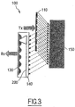
- FIG. 3 a device for controlling a material 150 in reflection mode is observed.
- the means and the operating principle are identical to that of the control device in transmission mode.
- the difference lies mainly in the relative arrangement of the transmission means 110, the modulation means 140 and the reception means 130.
- the transmission means 110 on the one hand and the modulation means 140 and reception means 130 on the other hand are arranged on the same side with respect to the material 150 to be controlled so that the modulation means 140 receive the signal reflected by the material 150.
- This device offers the advantage of operating in double transmission since in this mode the electromagnetic signal at the frequency of the carrier passes twice through the material 150 under test.
- This type of device has an advantage in the case of lack of access to one side of the material 150 to be measured and in the case where the material 150 to be tested has a metallized face.
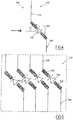
- the spatial modulation sensor 200 shown in FIG. figure 4 consists of four main elements, namely a set of radiating strands 220, a nonlinear electronic component 230, supply wires 240 and a substrate 210.
- the operating principle of a sensor 200 is described for the sensors 200 of the modulation means 140 present on the signal path between the material 150 and the receiving means 130. It is as follows.
- the radiating strands 220 of the sensor 200 will pick up the electromagnetic signals at the frequency of the carrier Fp having passed through the material 150.
- these strands 220 are loaded by the nonlinear electronic component 230 itself polarized using a signal at the modulation frequency Fm2.
- each sensor 200 comprises two radiating strands 220 each connected on either side of the non-linear electronic component 230.
- the nonlinear electronic component 230 is preferably an electrical or photoelectric diode.
- It can also be a temperature-sensitive non-linear component of the thermistor type.
- the modulation efficiency of the sensor 200 is directly related to the contrast between the on state and the off state of the diode.
- the two radiating strands 220 are preferably in the form of a rectangular segment. In a variant, other shapes are possible for the radiating strands 220.
- the size of the strands 220 is preferably small in front of the wavelength.
- these strands 220 are positioned in an angular configuration determined with respect to the direction of polarization of the antenna array of the transmission means 110.
- the angle ⁇ formed between the longitudinal direction of the strands and the direction of polarization of the network of antennas can be between 0 ° and 180 °.
- Each sensor 200 further comprises two power supply wires 240 supplying the non-linear electronic component 230, these supply wires 240 being preferably arranged perpendicularly to the direction of polarization of the antenna array of the transmission means 110.
- the substrate 210 on which the rest of the other elements rests may be flexible or rigid. It advantageously has dielectric properties and a small thickness to limit the reflections at the interface and the amplitude losses of incident electromagnetic signal.
- shaped configurations of the sensor arrays 200 can be envisaged.
- a network of circular type sensors 200 will adapt to the control of a moving material in a tube for example.
- the modulating elements 230 integrated in the sensors 200 are preferably non-linear electrical or electro-optical components.
- the queues 240 may be printed or unprinted electrical son and in the case of electro-optical sensors, the supply son 240 are replaced by optical fibers or a laser beam.
- the length of the network must be equal to or greater than the width of the material 150 to be controlled in order to be able to control it entirely.
- These sensors 200 of the network are preferably equidistant in pairs. They are more precisely spaced a particular distance D to define the spatial resolution of the device.
- the arrayed sensors 200 may each have different dimensions and angular positions with respect to the polarization of the antenna array of the transmission means 110.
- Another alternative embodiment consists in using an arrangement of several non-linear electronic components 230, for example, in series and loading the strands 220 of the sensor.
- Another variant embodiment consists of breaking up the strands 220 of the sensor which are loaded by an arrangement of several non-linear electronic components 230.
- an alternative embodiment provides a stack of two sensors 200 having two different angular positions with respect to the polarization of the antenna array of the transmission means 110. This makes it possible to obtain a bipolarization of the global sensor 200 formed and be able to measure the two components of the incident electromagnetic field in coincidence locally.
- Another alternative embodiment provides for implementing antennas of bipolarized transmission and / or reception means in combination with bipolarized sensors so as to perform polarimetric measurements of defects in the materials.
Landscapes
- Physics & Mathematics (AREA)
- General Health & Medical Sciences (AREA)
- Immunology (AREA)
- Chemical & Material Sciences (AREA)
- Analytical Chemistry (AREA)
- Biochemistry (AREA)
- Health & Medical Sciences (AREA)
- General Physics & Mathematics (AREA)
- Life Sciences & Earth Sciences (AREA)
- Pathology (AREA)
- Electromagnetism (AREA)
- Variable-Direction Aerials And Aerial Arrays (AREA)
- Radar Systems Or Details Thereof (AREA)
- Arrangements For Transmission Of Measured Signals (AREA)
- Geophysics And Detection Of Objects (AREA)
Applications Claiming Priority (2)
| Application Number | Priority Date | Filing Date | Title |
|---|---|---|---|
| FR0608398A FR2906369B1 (fr) | 2006-09-25 | 2006-09-25 | Dispositif micro-onde de controle d'un materiau |
| PCT/EP2007/060150 WO2008037705A1 (fr) | 2006-09-25 | 2007-09-25 | Dispositif micro-onde de controle d'un materiau |
Publications (2)
| Publication Number | Publication Date |
|---|---|
| EP2074411A1 EP2074411A1 (fr) | 2009-07-01 |
| EP2074411B1 true EP2074411B1 (fr) | 2016-03-30 |
Family
ID=37908329
Family Applications (1)
| Application Number | Title | Priority Date | Filing Date |
|---|---|---|---|
| EP07803601.9A Active EP2074411B1 (fr) | 2006-09-25 | 2007-09-25 | Dispositif micro-onde de controle d'un materiau |
Country Status (12)
| Country | Link |
|---|---|
| US (1) | US8093912B2 (pt) |
| EP (1) | EP2074411B1 (pt) |
| JP (1) | JP5030185B2 (pt) |
| CN (1) | CN101627299B (pt) |
| AU (1) | AU2007302051B2 (pt) |
| BR (1) | BRPI0715261B1 (pt) |
| CA (1) | CA2664544C (pt) |
| ES (1) | ES2574978T3 (pt) |
| FR (1) | FR2906369B1 (pt) |
| PL (1) | PL2074411T3 (pt) |
| RU (1) | RU2496105C2 (pt) |
| WO (1) | WO2008037705A1 (pt) |
Families Citing this family (4)
| Publication number | Priority date | Publication date | Assignee | Title |
|---|---|---|---|---|
| FI124138B (fi) * | 2008-04-21 | 2014-03-31 | Smartrac Ip Bv | Menetelmä rullattavan rainan valmistamiseksi ja rullattava raina |
| FR2983419B1 (fr) | 2011-12-06 | 2017-05-19 | Pellenc Selective Tech | Procede et installation d'inspection et/ou de tri combinant analyse de surface et analyse volumique |
| CN109324066B (zh) * | 2019-01-02 | 2019-06-04 | 湖南赛博诺格电子科技有限公司 | 一种合成板材批量检测方法 |
| KR102733247B1 (ko) * | 2022-11-30 | 2024-11-25 | 한국생산기술연구원 | 빌지오일 검출 장치 |
Family Cites Families (12)
| Publication number | Priority date | Publication date | Assignee | Title |
|---|---|---|---|---|
| FR2509064A1 (fr) * | 1981-07-02 | 1983-01-07 | Centre Nat Rech Scient | Procede et dispositif d'imagerie rapide en microonde |
| FR2614419B1 (fr) * | 1987-04-21 | 1989-06-16 | Centre Nat Rech Scient | Dispositif de mesure, en une pluralite de points, du champ micro-onde diffracte par un objet |
| US5353799A (en) * | 1991-01-22 | 1994-10-11 | Non Invasive Technology, Inc. | Examination of subjects using photon migration with high directionality techniques |
| US5619143A (en) * | 1989-02-14 | 1997-04-08 | Commonwealth Scientific And Industrial Research Organisation | Microwave scanning apparatus |
| CA2078056C (en) * | 1990-03-23 | 2002-07-30 | Nicholas George Cutmore | Determination of carbon in fly ash |
| US5715819A (en) * | 1994-05-26 | 1998-02-10 | The Carolinas Heart Institute | Microwave tomographic spectroscopy system and method |
| US5581256A (en) * | 1994-09-06 | 1996-12-03 | The Regents Of The University Of California | Range gated strip proximity sensor |
| US5841288A (en) * | 1996-02-12 | 1998-11-24 | Microwave Imaging System Technologies, Inc. | Two-dimensional microwave imaging apparatus and methods |
| JP4709421B2 (ja) * | 2001-04-27 | 2011-06-22 | 三井造船株式会社 | マルチパス3次元映像化レーダ装置 |
| JP2004333344A (ja) * | 2003-05-09 | 2004-11-25 | Hitachi Ltd | 光計測方法および装置 |
| US7541602B2 (en) * | 2007-06-04 | 2009-06-02 | Or-Nim Medical Ltd. | System and method for noninvasively monitoring conditions of a subject |
| EP2110076A1 (en) * | 2008-02-19 | 2009-10-21 | Helmholtz Zentrum München Deutsches Forschungszentrum für Gesundheit und Umwelt (GmbH) | Method and device for near-field dual-wave modality imaging |
-
2006
- 2006-09-25 FR FR0608398A patent/FR2906369B1/fr active Active
-
2007
- 2007-09-25 AU AU2007302051A patent/AU2007302051B2/en active Active
- 2007-09-25 WO PCT/EP2007/060150 patent/WO2008037705A1/fr not_active Ceased
- 2007-09-25 RU RU2009115372/07A patent/RU2496105C2/ru active
- 2007-09-25 EP EP07803601.9A patent/EP2074411B1/fr active Active
- 2007-09-25 CN CN2007800391658A patent/CN101627299B/zh active Active
- 2007-09-25 US US12/442,909 patent/US8093912B2/en active Active
- 2007-09-25 BR BRPI0715261-2A patent/BRPI0715261B1/pt active IP Right Grant
- 2007-09-25 PL PL07803601.9T patent/PL2074411T3/pl unknown
- 2007-09-25 CA CA2664544A patent/CA2664544C/fr active Active
- 2007-09-25 JP JP2009529687A patent/JP5030185B2/ja active Active
- 2007-09-25 ES ES07803601.9T patent/ES2574978T3/es active Active
Also Published As
| Publication number | Publication date |
|---|---|
| US20100005891A1 (en) | 2010-01-14 |
| CA2664544A1 (fr) | 2008-04-03 |
| EP2074411A1 (fr) | 2009-07-01 |
| FR2906369B1 (fr) | 2009-03-06 |
| BRPI0715261A2 (pt) | 2013-06-11 |
| BRPI0715261B1 (pt) | 2018-07-10 |
| AU2007302051A1 (en) | 2008-04-03 |
| PL2074411T3 (pl) | 2016-09-30 |
| ES2574978T3 (es) | 2016-06-23 |
| JP5030185B2 (ja) | 2012-09-19 |
| WO2008037705A1 (fr) | 2008-04-03 |
| CN101627299A (zh) | 2010-01-13 |
| CN101627299B (zh) | 2012-11-28 |
| FR2906369A1 (fr) | 2008-03-28 |
| RU2009115372A (ru) | 2010-11-10 |
| HK1138907A1 (en) | 2010-09-03 |
| JP2010504535A (ja) | 2010-02-12 |
| AU2007302051B2 (en) | 2013-09-12 |
| RU2496105C2 (ru) | 2013-10-20 |
| CA2664544C (fr) | 2016-06-07 |
| US8093912B2 (en) | 2012-01-10 |
Similar Documents
| Publication | Publication Date | Title |
|---|---|---|
| EP2869399B1 (fr) | Etalonnage d'un réseau d'antennes | |
| EP0354115B1 (fr) | Dispositif d'émission et de réception d'un rayonnement micro-onde, pour imagerie d'objets enfouis | |
| EP0355114B1 (fr) | Dispositif de mesure, en une pluralite de points, du champ micro-onde diffracte par un objet | |
| EP0533785B1 (fr) | Dispositif de mesure, en une pluralite de points d'une surface du champ micro-onde rayonne par une source | |
| WO2007088176A1 (fr) | Source lumineuse étendue et électriquement modulable, dispositif de mesure pour caractériser un semi-conducteur comportant une telle source | |
| CA2664544C (fr) | Dispositif micro-onde de controle d'un materiau | |
| FR2924234A1 (fr) | Canal de tres haute qualite pour les joints tournants optiques multivoies. | |
| CN117571042A (zh) | 一种海底电缆状态采集装置及方法 | |
| FR2977683A1 (fr) | Dispositif pour detecter des objets tels que des mines | |
| FR2780794A1 (fr) | Velocimetre holographique dynamique pour la mesure de vibrations | |
| EP2208016B1 (fr) | Capteur optique pour mesurer la deformation au cours du temps d'une structure plane deformable | |
| EP0772047B1 (fr) | Dispositif de mesure de champ électrique | |
| FR2990271B1 (fr) | Controle par ultrasons laser de pieces a reflectivite speculaire base sur une detection a deux niveaux de sensibilite | |
| WO2025052337A1 (fr) | Procédés et systèmes de contrôle non destructif d'un séparateur pour cellules de batterie | |
| FR2943426A1 (fr) | Dispositif electro-optique integre de mesure de champ electromagnetique | |
| FR2879752A1 (fr) | Sonde electro-optique de mesure de champs electriques ou electromagnetiques a asservissement optique par la longueur d'onde du point de fonctionnement | |
| EP3400488A2 (fr) | Dispositif d'imagerie du champs électromagnétique d'un échantillon | |
| WO2010012843A1 (fr) | Capteur polarimétrique pour la mesure de la déformation subie par une surface | |
| FR3095519A1 (fr) | Procédé non-invasif de détermination du genre d'un œuf | |
| HK1138907B (en) | Device and method for controlling a material | |
| FR2722571A1 (fr) | Procede de caracterisation d'un instrument optique par auto-collimation et instrument permettant sa mise en oeuvre | |
| FR2922317A1 (fr) | Dispositif de mesure hyperfrequence pour test a distance d'une ligne hyperfrequence |
Legal Events
| Date | Code | Title | Description |
|---|---|---|---|
| PUAI | Public reference made under article 153(3) epc to a published international application that has entered the european phase |
Free format text: ORIGINAL CODE: 0009012 |
|
| 17P | Request for examination filed |
Effective date: 20090420 |
|
| AK | Designated contracting states |
Kind code of ref document: A1 Designated state(s): AT BE BG CH CY CZ DE DK EE ES FI FR GB GR HU IE IS IT LI LT LU LV MC MT NL PL PT RO SE SI SK TR |
|
| RIN1 | Information on inventor provided before grant (corrected) |
Inventor name: ROBIC, NICOLAS Inventor name: IVERSEN, PER Inventor name: TESSIER, VIRGINIE Inventor name: DURAND, LUDOVIC Inventor name: GANDOIS, ARNAUD Inventor name: DUCHESNE, LUC Inventor name: DREAN, JEROME Inventor name: GARREAU, PHILIPPE |
|
| 17Q | First examination report despatched |
Effective date: 20110523 |
|
| DAX | Request for extension of the european patent (deleted) | ||
| RAP1 | Party data changed (applicant data changed or rights of an application transferred) |
Owner name: MICROWAVE VISION |
|
| GRAP | Despatch of communication of intention to grant a patent |
Free format text: ORIGINAL CODE: EPIDOSNIGR1 |
|
| INTG | Intention to grant announced |
Effective date: 20151028 |
|
| GRAS | Grant fee paid |
Free format text: ORIGINAL CODE: EPIDOSNIGR3 |
|
| GRAA | (expected) grant |
Free format text: ORIGINAL CODE: 0009210 |
|
| AK | Designated contracting states |
Kind code of ref document: B1 Designated state(s): AT BE BG CH CY CZ DE DK EE ES FI FR GB GR HU IE IS IT LI LT LU LV MC MT NL PL PT RO SE SI SK TR |
|
| REG | Reference to a national code |
Ref country code: GB Ref legal event code: FG4D Free format text: NOT ENGLISH |
|
| REG | Reference to a national code |
Ref country code: CH Ref legal event code: EP |
|
| REG | Reference to a national code |
Ref country code: AT Ref legal event code: REF Ref document number: 785917 Country of ref document: AT Kind code of ref document: T Effective date: 20160415 |
|
| REG | Reference to a national code |
Ref country code: IE Ref legal event code: FG4D Free format text: LANGUAGE OF EP DOCUMENT: FRENCH |
|
| REG | Reference to a national code |
Ref country code: DE Ref legal event code: R096 Ref document number: 602007045558 Country of ref document: DE |
|
| REG | Reference to a national code |
Ref country code: ES Ref legal event code: FG2A Ref document number: 2574978 Country of ref document: ES Kind code of ref document: T3 Effective date: 20160623 |
|
| REG | Reference to a national code |
Ref country code: NL Ref legal event code: FP |
|
| REG | Reference to a national code |
Ref country code: LT Ref legal event code: MG4D |
|
| PG25 | Lapsed in a contracting state [announced via postgrant information from national office to epo] |
Ref country code: GR Free format text: LAPSE BECAUSE OF FAILURE TO SUBMIT A TRANSLATION OF THE DESCRIPTION OR TO PAY THE FEE WITHIN THE PRESCRIBED TIME-LIMIT Effective date: 20160701 Ref country code: FI Free format text: LAPSE BECAUSE OF FAILURE TO SUBMIT A TRANSLATION OF THE DESCRIPTION OR TO PAY THE FEE WITHIN THE PRESCRIBED TIME-LIMIT Effective date: 20160330 |
|
| REG | Reference to a national code |
Ref country code: AT Ref legal event code: MK05 Ref document number: 785917 Country of ref document: AT Kind code of ref document: T Effective date: 20160330 |
|
| PG25 | Lapsed in a contracting state [announced via postgrant information from national office to epo] |
Ref country code: SE Free format text: LAPSE BECAUSE OF FAILURE TO SUBMIT A TRANSLATION OF THE DESCRIPTION OR TO PAY THE FEE WITHIN THE PRESCRIBED TIME-LIMIT Effective date: 20160330 Ref country code: LV Free format text: LAPSE BECAUSE OF FAILURE TO SUBMIT A TRANSLATION OF THE DESCRIPTION OR TO PAY THE FEE WITHIN THE PRESCRIBED TIME-LIMIT Effective date: 20160330 Ref country code: LT Free format text: LAPSE BECAUSE OF FAILURE TO SUBMIT A TRANSLATION OF THE DESCRIPTION OR TO PAY THE FEE WITHIN THE PRESCRIBED TIME-LIMIT Effective date: 20160330 |
|
| REG | Reference to a national code |
Ref country code: FR Ref legal event code: PLFP Year of fee payment: 10 |
|
| PG25 | Lapsed in a contracting state [announced via postgrant information from national office to epo] |
Ref country code: EE Free format text: LAPSE BECAUSE OF FAILURE TO SUBMIT A TRANSLATION OF THE DESCRIPTION OR TO PAY THE FEE WITHIN THE PRESCRIBED TIME-LIMIT Effective date: 20160330 Ref country code: IS Free format text: LAPSE BECAUSE OF FAILURE TO SUBMIT A TRANSLATION OF THE DESCRIPTION OR TO PAY THE FEE WITHIN THE PRESCRIBED TIME-LIMIT Effective date: 20160730 |
|
| PG25 | Lapsed in a contracting state [announced via postgrant information from national office to epo] |
Ref country code: SK Free format text: LAPSE BECAUSE OF FAILURE TO SUBMIT A TRANSLATION OF THE DESCRIPTION OR TO PAY THE FEE WITHIN THE PRESCRIBED TIME-LIMIT Effective date: 20160330 Ref country code: PT Free format text: LAPSE BECAUSE OF FAILURE TO SUBMIT A TRANSLATION OF THE DESCRIPTION OR TO PAY THE FEE WITHIN THE PRESCRIBED TIME-LIMIT Effective date: 20160801 Ref country code: AT Free format text: LAPSE BECAUSE OF FAILURE TO SUBMIT A TRANSLATION OF THE DESCRIPTION OR TO PAY THE FEE WITHIN THE PRESCRIBED TIME-LIMIT Effective date: 20160330 Ref country code: RO Free format text: LAPSE BECAUSE OF FAILURE TO SUBMIT A TRANSLATION OF THE DESCRIPTION OR TO PAY THE FEE WITHIN THE PRESCRIBED TIME-LIMIT Effective date: 20160330 |
|
| REG | Reference to a national code |
Ref country code: DE Ref legal event code: R097 Ref document number: 602007045558 Country of ref document: DE |
|
| PG25 | Lapsed in a contracting state [announced via postgrant information from national office to epo] |
Ref country code: DK Free format text: LAPSE BECAUSE OF FAILURE TO SUBMIT A TRANSLATION OF THE DESCRIPTION OR TO PAY THE FEE WITHIN THE PRESCRIBED TIME-LIMIT Effective date: 20160330 |
|
| PLBE | No opposition filed within time limit |
Free format text: ORIGINAL CODE: 0009261 |
|
| STAA | Information on the status of an ep patent application or granted ep patent |
Free format text: STATUS: NO OPPOSITION FILED WITHIN TIME LIMIT |
|
| 26N | No opposition filed |
Effective date: 20170103 |
|
| PG25 | Lapsed in a contracting state [announced via postgrant information from national office to epo] |
Ref country code: MC Free format text: LAPSE BECAUSE OF FAILURE TO SUBMIT A TRANSLATION OF THE DESCRIPTION OR TO PAY THE FEE WITHIN THE PRESCRIBED TIME-LIMIT Effective date: 20160330 |
|
| REG | Reference to a national code |
Ref country code: CH Ref legal event code: PL |
|
| PG25 | Lapsed in a contracting state [announced via postgrant information from national office to epo] |
Ref country code: SI Free format text: LAPSE BECAUSE OF FAILURE TO SUBMIT A TRANSLATION OF THE DESCRIPTION OR TO PAY THE FEE WITHIN THE PRESCRIBED TIME-LIMIT Effective date: 20160330 |
|
| REG | Reference to a national code |
Ref country code: IE Ref legal event code: MM4A |
|
| PG25 | Lapsed in a contracting state [announced via postgrant information from national office to epo] |
Ref country code: CH Free format text: LAPSE BECAUSE OF NON-PAYMENT OF DUE FEES Effective date: 20160930 Ref country code: IE Free format text: LAPSE BECAUSE OF NON-PAYMENT OF DUE FEES Effective date: 20160925 Ref country code: LI Free format text: LAPSE BECAUSE OF NON-PAYMENT OF DUE FEES Effective date: 20160930 |
|
| PG25 | Lapsed in a contracting state [announced via postgrant information from national office to epo] |
Ref country code: LU Free format text: LAPSE BECAUSE OF NON-PAYMENT OF DUE FEES Effective date: 20160925 |
|
| REG | Reference to a national code |
Ref country code: FR Ref legal event code: PLFP Year of fee payment: 11 |
|
| PG25 | Lapsed in a contracting state [announced via postgrant information from national office to epo] |
Ref country code: CY Free format text: LAPSE BECAUSE OF FAILURE TO SUBMIT A TRANSLATION OF THE DESCRIPTION OR TO PAY THE FEE WITHIN THE PRESCRIBED TIME-LIMIT Effective date: 20160330 Ref country code: HU Free format text: LAPSE BECAUSE OF FAILURE TO SUBMIT A TRANSLATION OF THE DESCRIPTION OR TO PAY THE FEE WITHIN THE PRESCRIBED TIME-LIMIT; INVALID AB INITIO Effective date: 20070925 |
|
| PG25 | Lapsed in a contracting state [announced via postgrant information from national office to epo] |
Ref country code: TR Free format text: LAPSE BECAUSE OF FAILURE TO SUBMIT A TRANSLATION OF THE DESCRIPTION OR TO PAY THE FEE WITHIN THE PRESCRIBED TIME-LIMIT Effective date: 20160330 Ref country code: MT Free format text: LAPSE BECAUSE OF FAILURE TO SUBMIT A TRANSLATION OF THE DESCRIPTION OR TO PAY THE FEE WITHIN THE PRESCRIBED TIME-LIMIT Effective date: 20160330 |
|
| PG25 | Lapsed in a contracting state [announced via postgrant information from national office to epo] |
Ref country code: BG Free format text: LAPSE BECAUSE OF FAILURE TO SUBMIT A TRANSLATION OF THE DESCRIPTION OR TO PAY THE FEE WITHIN THE PRESCRIBED TIME-LIMIT Effective date: 20160330 |
|
| REG | Reference to a national code |
Ref country code: FR Ref legal event code: PLFP Year of fee payment: 12 |
|
| REG | Reference to a national code |
Ref country code: DE Ref legal event code: R081 Ref document number: 602007045558 Country of ref document: DE Owner name: MICROWAVE VISION, FR Free format text: FORMER OWNER: MICROWAVE VISION, VILLEBON SUR YVETTE, FR |
|
| REG | Reference to a national code |
Ref country code: DE Ref legal event code: R082 Ref document number: 602007045558 Country of ref document: DE Representative=s name: KILIAN KILIAN & PARTNER MBB PATENTANWAELTE, DE |
|
| PGFP | Annual fee paid to national office [announced via postgrant information from national office to epo] |
Ref country code: DE Payment date: 20250916 Year of fee payment: 19 |
|
| PGFP | Annual fee paid to national office [announced via postgrant information from national office to epo] |
Ref country code: PL Payment date: 20250821 Year of fee payment: 19 Ref country code: NL Payment date: 20250909 Year of fee payment: 19 Ref country code: IT Payment date: 20250910 Year of fee payment: 19 |
|
| PGFP | Annual fee paid to national office [announced via postgrant information from national office to epo] |
Ref country code: BE Payment date: 20250919 Year of fee payment: 19 Ref country code: GB Payment date: 20250919 Year of fee payment: 19 |
|
| PGFP | Annual fee paid to national office [announced via postgrant information from national office to epo] |
Ref country code: FR Payment date: 20250812 Year of fee payment: 19 |
|
| PGFP | Annual fee paid to national office [announced via postgrant information from national office to epo] |
Ref country code: CZ Payment date: 20250925 Year of fee payment: 19 |
|
| PGFP | Annual fee paid to national office [announced via postgrant information from national office to epo] |
Ref country code: ES Payment date: 20251015 Year of fee payment: 19 |