EP2074454B1 - Procédé pour le couplage par fusion induite au laser d'une fibre optique à un guide d'ondes optique - Google Patents
Procédé pour le couplage par fusion induite au laser d'une fibre optique à un guide d'ondes optique Download PDFInfo
- Publication number
- EP2074454B1 EP2074454B1 EP07825075.0A EP07825075A EP2074454B1 EP 2074454 B1 EP2074454 B1 EP 2074454B1 EP 07825075 A EP07825075 A EP 07825075A EP 2074454 B1 EP2074454 B1 EP 2074454B1
- Authority
- EP
- European Patent Office
- Prior art keywords
- fiber
- optical
- laser
- optical fiber
- bulk material
- Prior art date
- Legal status (The legal status is an assumption and is not a legal conclusion. Google has not performed a legal analysis and makes no representation as to the accuracy of the status listed.)
- Not-in-force
Links
- 230000003287 optical effect Effects 0.000 title claims description 37
- 238000000034 method Methods 0.000 title claims description 34
- 239000013307 optical fiber Substances 0.000 title claims description 28
- 230000004927 fusion Effects 0.000 title description 8
- 239000013590 bulk material Substances 0.000 claims description 27
- 230000005855 radiation Effects 0.000 claims description 13
- 229910052751 metal Inorganic materials 0.000 claims description 9
- 239000002184 metal Substances 0.000 claims description 9
- PXHVJJICTQNCMI-UHFFFAOYSA-N Nickel Chemical compound [Ni] PXHVJJICTQNCMI-UHFFFAOYSA-N 0.000 claims description 8
- 230000003667 anti-reflective effect Effects 0.000 claims description 4
- 230000005684 electric field Effects 0.000 claims description 4
- PCHJSUWPFVWCPO-UHFFFAOYSA-N gold Chemical compound [Au] PCHJSUWPFVWCPO-UHFFFAOYSA-N 0.000 claims description 4
- 229910052737 gold Inorganic materials 0.000 claims description 4
- 239000010931 gold Substances 0.000 claims description 4
- 229910052759 nickel Inorganic materials 0.000 claims description 4
- VYZAMTAEIAYCRO-UHFFFAOYSA-N Chromium Chemical compound [Cr] VYZAMTAEIAYCRO-UHFFFAOYSA-N 0.000 claims description 3
- BQCADISMDOOEFD-UHFFFAOYSA-N Silver Chemical compound [Ag] BQCADISMDOOEFD-UHFFFAOYSA-N 0.000 claims description 3
- 229910045601 alloy Inorganic materials 0.000 claims description 3
- 239000000956 alloy Substances 0.000 claims description 3
- 229910052782 aluminium Inorganic materials 0.000 claims description 3
- XAGFODPZIPBFFR-UHFFFAOYSA-N aluminium Chemical compound [Al] XAGFODPZIPBFFR-UHFFFAOYSA-N 0.000 claims description 3
- 229910052804 chromium Inorganic materials 0.000 claims description 3
- 239000011651 chromium Substances 0.000 claims description 3
- 238000010891 electric arc Methods 0.000 claims description 3
- 150000002739 metals Chemical class 0.000 claims description 3
- 229910052703 rhodium Inorganic materials 0.000 claims description 3
- 239000010948 rhodium Substances 0.000 claims description 3
- MHOVAHRLVXNVSD-UHFFFAOYSA-N rhodium atom Chemical compound [Rh] MHOVAHRLVXNVSD-UHFFFAOYSA-N 0.000 claims description 3
- 229910052709 silver Inorganic materials 0.000 claims description 3
- 239000004332 silver Substances 0.000 claims description 3
- 230000001154 acute effect Effects 0.000 claims description 2
- 239000000835 fiber Substances 0.000 description 46
- 239000010410 layer Substances 0.000 description 35
- 238000005253 cladding Methods 0.000 description 10
- 239000004593 Epoxy Substances 0.000 description 8
- 238000005304 joining Methods 0.000 description 6
- 239000000463 material Substances 0.000 description 6
- 239000004020 conductor Substances 0.000 description 5
- 238000010438 heat treatment Methods 0.000 description 5
- 238000002844 melting Methods 0.000 description 5
- 230000008018 melting Effects 0.000 description 5
- 230000008569 process Effects 0.000 description 5
- VYPSYNLAJGMNEJ-UHFFFAOYSA-N Silicium dioxide Chemical compound O=[Si]=O VYPSYNLAJGMNEJ-UHFFFAOYSA-N 0.000 description 4
- 238000005516 engineering process Methods 0.000 description 4
- 238000003780 insertion Methods 0.000 description 4
- 230000037431 insertion Effects 0.000 description 4
- 230000015556 catabolic process Effects 0.000 description 3
- 239000002105 nanoparticle Substances 0.000 description 3
- 239000000758 substrate Substances 0.000 description 3
- 239000006117 anti-reflective coating Substances 0.000 description 2
- 230000005540 biological transmission Effects 0.000 description 2
- 239000011248 coating agent Substances 0.000 description 2
- 238000000576 coating method Methods 0.000 description 2
- 238000004891 communication Methods 0.000 description 2
- 239000003989 dielectric material Substances 0.000 description 2
- 238000007526 fusion splicing Methods 0.000 description 2
- 239000011521 glass Substances 0.000 description 2
- 239000002052 molecular layer Substances 0.000 description 2
- 239000002245 particle Substances 0.000 description 2
- 230000001902 propagating effect Effects 0.000 description 2
- 239000000377 silicon dioxide Substances 0.000 description 2
- 230000003595 spectral effect Effects 0.000 description 2
- 239000006096 absorbing agent Substances 0.000 description 1
- 238000010521 absorption reaction Methods 0.000 description 1
- 230000002411 adverse Effects 0.000 description 1
- 238000000137 annealing Methods 0.000 description 1
- 238000005452 bending Methods 0.000 description 1
- 230000008033 biological extinction Effects 0.000 description 1
- 239000011247 coating layer Substances 0.000 description 1
- 229910017052 cobalt Inorganic materials 0.000 description 1
- 239000010941 cobalt Substances 0.000 description 1
- GUTLYIVDDKVIGB-UHFFFAOYSA-N cobalt atom Chemical compound [Co] GUTLYIVDDKVIGB-UHFFFAOYSA-N 0.000 description 1
- 230000008878 coupling Effects 0.000 description 1
- 238000010168 coupling process Methods 0.000 description 1
- 238000005859 coupling reaction Methods 0.000 description 1
- 238000000151 deposition Methods 0.000 description 1
- 238000009826 distribution Methods 0.000 description 1
- -1 e.g. Substances 0.000 description 1
- 229920006332 epoxy adhesive Polymers 0.000 description 1
- 238000007499 fusion processing Methods 0.000 description 1
- 230000008570 general process Effects 0.000 description 1
- 230000001678 irradiating effect Effects 0.000 description 1
- 238000004093 laser heating Methods 0.000 description 1
- 230000031700 light absorption Effects 0.000 description 1
- 238000010943 off-gassing Methods 0.000 description 1
- 238000004806 packaging method and process Methods 0.000 description 1
- 230000002093 peripheral effect Effects 0.000 description 1
- 239000000843 powder Substances 0.000 description 1
- 239000002356 single layer Substances 0.000 description 1
- 239000007787 solid Substances 0.000 description 1
- 238000001228 spectrum Methods 0.000 description 1
- 239000011800 void material Substances 0.000 description 1
- 239000002699 waste material Substances 0.000 description 1
Images

Classifications
-
- G—PHYSICS
- G02—OPTICS
- G02B—OPTICAL ELEMENTS, SYSTEMS OR APPARATUS
- G02B6/00—Light guides; Structural details of arrangements comprising light guides and other optical elements, e.g. couplings
- G02B6/24—Coupling light guides
- G02B6/255—Splicing of light guides, e.g. by fusion or bonding
- G02B6/2551—Splicing of light guides, e.g. by fusion or bonding using thermal methods, e.g. fusion welding by arc discharge, laser beam, plasma torch
-
- G—PHYSICS
- G02—OPTICS
- G02B—OPTICAL ELEMENTS, SYSTEMS OR APPARATUS
- G02B6/00—Light guides; Structural details of arrangements comprising light guides and other optical elements, e.g. couplings
- G02B6/24—Coupling light guides
- G02B6/26—Optical coupling means
- G02B6/30—Optical coupling means for use between fibre and thin-film device
-
- G—PHYSICS
- G02—OPTICS
- G02B—OPTICAL ELEMENTS, SYSTEMS OR APPARATUS
- G02B6/00—Light guides; Structural details of arrangements comprising light guides and other optical elements, e.g. couplings
- G02B6/24—Coupling light guides
- G02B6/42—Coupling light guides with opto-electronic elements
- G02B6/4201—Packages, e.g. shape, construction, internal or external details
- G02B6/4204—Packages, e.g. shape, construction, internal or external details the coupling comprising intermediate optical elements, e.g. lenses, holograms
- G02B6/4207—Packages, e.g. shape, construction, internal or external details the coupling comprising intermediate optical elements, e.g. lenses, holograms with optical elements reducing the sensitivity to optical feedback
Definitions
- the present invention generally relates to the field of fiber optical communications, and more particularly to methods for joining optical fibers with integrated optical waveguides.
- Joining or splicing of optical fibers to optical fibers or optical waveguides on bulk material is of major importance in most fiber optics devices.
- the most common technology for fiber joining is fusion splicing, using an electrical arc short pulse for heating the two fiber ends while being spliced.
- This technology is applicable to fibers of equal diameters, but is not applicable for fiber to optical waveguides or bulk material attachment, since the bulk dimensions are much larger than the fiber and arc splicing cannot heat both the fiber and the optical waveguides or bulk material attachment equally and get an equal layer melted on both surfaces of the optical splice.
- Epoxy adhesive or simply epoxy is the predominant current bonding technology.
- the epoxy is introduced between the fiber and appropriate optical waveguides port and cured with the help of UV radiation.
- Epoxy serves not only as a bonding material; it enables some refractive index matching reducing transmission losses.
- the method suffers of a number of shortcomings: Curing of the epoxy is not uniform; epoxy curing time is relatively long and the fiber frequently changes its position after alignment; epoxy out gassing adversely affects the hermetic photonic element packaging, and the optical transmission of the epoxy changes with the time. Since light passes through the epoxy, high power applications are prohibited. This procedure of splicing is a multi-step process, requiring a relatively long time. Some temporary splices use index-matching gel between the two surfaces, and need a permanent mechanical set up for aligning.
- U.S. Pat. No. 6,296,401 to Paris and U.S. Pat. No. 6,411,759 to Beguin et al. disclose methods of optical fiber to waveguide connection by fusion.
- Paris shows a method for fusion pigtailing of an optical fiber to an integrated optical device with an optical device formed on a substrate.
- the substrate includes a groove under and behind an interface between the optical fiber and the optical device. Provision of such a groove allows the substrate to be used for alignment and support of the optical fiber, while reducing optical insertion loss and improving durability of the interface. Paris does not disclose the method according to which fiber fusion is performed.
- Beguin shows a fusion joint between a waveguide and an optical fiber created by irradiating the interface between the optical fiber and the waveguide using a laser beam.
- the spatial distribution of the energy furnished to the interface presents a central zone of which the energy is reduced with respect to a peripheral zone, whereby to enable a relatively high-energy laser to be used while avoiding bending of the waveguide by high power laser heating.
- the laser beam is caused to irradiate a higher energy density upon the waveguide than the optical fiber, typically by offsetting the center of the laser beam towards the waveguide.
- the fusion is performed by the heat generated by the laser light absorption, while a force F urges the waveguide and optical fiber towards one another, to avoid the creation of a void at the boundary.
- U.S. Pat. No. 6,360,039 to Bernard et al. discloses a method of joining at least two optical components.
- One of the optical components having a surface that has a comparatively larger cross-sectional area than the surface of the other optical component e.g. an optical fiber.
- the optical components are joined together by fusion-splicing, using a laser for heating.
- the fusion is achieved by melting a small area surrounding the joint with the fiber section on the larger than the optical fiber component by a process where the larger surface is first pre-heated by the laser.
- the pre-heat temperature is just sufficient to polish and melt the surface of the larger component at the location one desires to fuse the smaller component.
- the second surface is then brought into contact with the preheated surface and, once the thermal exchange is established (by conduction of heat), all components are heated simultaneously. This process requires a long time and needs customization for each geometry.
- U.S. Pat. Application No. 20050180695 to Bronstein et al. discloses a method of joining a fiber and waveguide using a laser through the fiber, where the fiber is coated with laser absorbing glass powder or a special laser absorbing dye. Realization of this method is very problematic since the splice contains many laser absorbing centers, remnants of the initial absorbers, the splice has very high insertion loss and high reflections making it unfit for optical communication.
- the laser light can be applied to the interface through the fiber core and cladding internally or through the bulk material externally.
- the electrical arc, generated by the laser electric field, is confined to the interface covered by the nanometric conductive layer and to the laser spot dimensions.
- a nanometric, electrically conductive layer exposed to the laser light
- the laser is a high power pulsed laser, e.g., in the 1.5 micron region or in other regions that are transmitted by the fiber.
- the laser is a high power CW laser, e.g., in the 1.5 micron region or in other regions that are transmitted by the bulk material.
- the laser is a high power pulsed laser, e.g., in the 1.5 micron region or in other spectral regions that are transmitted by the fiber.
- the laser is a high power pulsed laser, e.g., in the 1.5 micron region or in other spectral regions that are transmitted by the bulk material.
- the objectives of the present invention may be achieved by a method of joining by laser fusion of an optical fiber to at least one port of a waveguide, comprising the steps of:
- a laser fused splice 2 composed of an optical waveguide, e.g., a solid waveguide or a fiber, split transversely to form two waveguide sections 4' and 4."
- Each of the waveguide sections 4' and 4" is composed of a central core 6, in which most of the light propagates, and an outer cladding 8.
- the waveguide section 4' has an input end 10 and the waveguide section 4" has an output end 12.
- a conducting layer 14 Interposed between the two waveguide sections 4' and 4", and traversing the path of optical energy propagating in the core from the input end 10 to the output end 12, is a conducting layer 14.
- the layer 14 is very thin (only a few atomic layers, typically between about 1 and about 20 nanometers) and is made of a conducting material, preferably a metal such as rhodium, aluminum, gold, silver, chromium or nickel, or a combination or alloy of such metals.
- a conducting material preferably a metal such as rhodium, aluminum, gold, silver, chromium or nickel, or a combination or alloy of such metals.
- Such thin layers of conducting material are known to enhance the electric field strength in their vicinity due to local irregularities of their surface, where the surface irregularities induce field concentration, resulting in lower power needed to create an electrical breakdown, arc discharge and melting.
- the thin layer of conducting material is impinged with optical power exceeding a predetermined threshold, strong electric fields, which can lead to local electrical breakdown, are generated at certain sites ("hot spots") in proximity with the conductive surface. This leads to a visible-light-emitting arc discharge and material melting.
- the melting on both sides of the thin layer creates a permanent splice, where most of the thin layer is diffused away and the optical loss is very low.
- Such thin nanometric layers may be modeled as a plurality of aggregates of nano-particles (see, e.g., M. Quinten, “Local Fields Close to the Surface of Nanoparticles and Aggregates of Nanoparticles," Appl. Phys. B 73, 245-255 (2001 ) and the book “ Absorption and Scattering of Light by Small Particles” by C.F. Bohren and D.R. Huffmann, Wiley-Interscience (1998), Chapter 12 [showing strong field enhancement factors (up to 10 5 ) for few-nanometer particles as well as wide extinction spectra for various materials and shapes].
- a low insertion loss at the operating powers is desirable, in order to avoid power losses.
- a conducting metallic layer generally absorbs and reflects some light. As discussed below, the reflection can be minimized by the addition of anti-reflective layers 16 and 18 on both sides of the conducting layer 14.
- the laser power for fusing is introduced in the core 6 or in the core 6 and cladding 8, which produces a larger surface of fused glass across the fiber.
- the conductive layer 14 can be deposited on a surface that extends across the optical waveguide at an acute angle, i.e., not perpendicular to the direction of propagation of the light, thus preventing any back reflection from re-entering the waveguide core, as depicted in FIG. 2 .
- the metal layer may be either a single layer or a layer that is covered on one or on both sides with transparent layers, which can serve as anti-reflective coatings, reducing the optical reflections.
- the coating layers 16 and 18 are designed to have minimal reflections.
- the anti-reflective layers 16 and 18 can be composed of the same dielectric material, or of two different materials. Generally, when using the same material, in order to obtain minimal reflection, the thicknesses of the layers 16 and 18 are unequal; the difference in thicknesses of the entry layer 16 and the exit layer 18 is due to a phase change of reflections from conducting surfaces as opposed to no phase change of reflections from dielectric material like the silica of the fiber.
- the coating is then an asymmetric coating, and has a pre-designated input direction.
- Each of the anti-reflective coatings 16, 18 preferably has a thickness within the range from about 0.1 to about 1.5 micrometer.
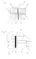
- FIG. 2 illustrates a device similar to that shown in Fig. 1 .
- the layers 14, 16 and 18 are not perpendicular to the direction of light propagation in the waveguide, but rather at an angle 20.
- the angle 20 is typically 8 degrees.
- an optical reflection 22 from the layer 14 does not propagate backwards inside the waveguide but assumes direction 22 absorbed in the cladding 8.
- FIG. 3 illustrates the welded fiber 28 similar to FIG. 1 packaged in an aligning sleeve 26 configuration and a ferrule 24 on each side.
- the fiber alignment prior to splicing by the laser is carried out by the aligning sleeve 26.
- the geometry is perpendicular.
- a conducting layer 14 Interposed between the two waveguide sections 4' and 4", and traversing the path of optical energy propagating in the core from the input end 10 to the output end 12, is a conducting layer 14.
- the layer 14 is very thin (only a few atomic layers, typically 1 to 20 nanometers) and is preferably made of a metal such as rhodium, aluminum, gold, silver, chromium or nickel, or a combination or alloy of such metals.
- FIG. 4 illustrates the splice of FIG.3 packaged in a sleeve 26 and ferrules 24 configuration.
- the two surfaces are at an angle and not perpendicular to the optical axis, called APC (Angled Physical Contact), for reflection reduction. All other parameters are similar to FIG. 3 .
- FIG. 5 illustrates a fiber to bulk material 32 splice, using a laser 34 through the bulk material or laser 38 through the fiber, for creation of the arc.
- the general process is similar to that described for FIG.1 .
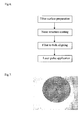
- FIG. 6 is a schematic flow chart of the process
- FIG. 7 is a microscope picture of a splice, having the following parameters: SMF 28 fiber, when spliced to another SMF 28 fiber using 2 watts, about 10 microsecond pulse, 1550 nm laser in the fiber core.
- the insertion loss is 1.3dB at start and is lowered to about 0.8 dB after splicing.
Landscapes
- Physics & Mathematics (AREA)
- General Physics & Mathematics (AREA)
- Optics & Photonics (AREA)
- Engineering & Computer Science (AREA)
- Plasma & Fusion (AREA)
- Mechanical Coupling Of Light Guides (AREA)
- Optical Couplings Of Light Guides (AREA)
Claims (8)
- Procédé de couplage instantané d'une fibre optique (43") à un guide d'onde optique (4') ou à un matériau en vrac (32), comprenant les étapes consistant à :former une couche nanométrique conductrice de l'électricité (14) sur les une ou deux surfaces à coupler entre ladite fibre optique (4") et ledit guide d'onde optique (4') ou ledit matériau en vrac (32) à coupler etappliquer un rayonnement laser (34, 38) auxdites une ou deux surfaces à coupler à travers ladite fibre optique (4") intérieurement ou à travers ledit matériau en vrac (32) extérieurement pour produire une décharge en arc due au champ électrique du laser.
- Procédé selon la revendication 1, dans lequel ladite couche conductrice (14) est au moins formée d'un métal choisi dans le groupe du rhodium, de l'aluminium, de l'or, de l'argent, du chrome, du nickel et des alliages desdits métaux.
- Procédé selon la revendication 1, dans lequel ladite couche conductrice (14) a une épaisseur entre environ 1 et environ 20 nanomètres.
- Procédé selon la revendication 1, qui comprend la formation de couches transparentes anti-réfléchissantes (16, 18) sur les côtés opposés de ladite couche conductrice (14) dans le trajet dudit rayonnement laser (34, 38).
- Procédé selon la revendication 4, dans lequel lesdites couches transparentes anti-réfléchissantes (16, 18) ont différentes épaisseurs.
- Procédé selon la revendication 1, dans lequel ladite couche conductrice (14) est déposée sur une surface qui s'étend en travers du trajet dudit rayonnement laser (34, 38) selon un angle aigu.
- Procédé selon la revendication 1, dans lequel ledit rayonnement laser (34, 38) est appliqué auxdites une ou deux surfaces à coupler à travers ladite fibre optique (4") intérieurement.
- Procédé selon la revendication 1, dans lequel ledit rayonnement laser est appliqué auxdites une ou deux surfaces à coupler à travers ledit matériau en vrac (32) extérieurement.
Applications Claiming Priority (2)
| Application Number | Priority Date | Filing Date | Title |
|---|---|---|---|
| US84399006P | 2006-09-12 | 2006-09-12 | |
| PCT/IB2007/002584 WO2008032165A2 (fr) | 2006-09-12 | 2007-09-07 | Procédé pour le couplage par fusion induite au laser d'une fibre optique à un guide d'ondes optique |
Publications (3)
| Publication Number | Publication Date |
|---|---|
| EP2074454A2 EP2074454A2 (fr) | 2009-07-01 |
| EP2074454A4 EP2074454A4 (fr) | 2012-11-28 |
| EP2074454B1 true EP2074454B1 (fr) | 2015-05-27 |
Family
ID=39184171
Family Applications (1)
| Application Number | Title | Priority Date | Filing Date |
|---|---|---|---|
| EP07825075.0A Not-in-force EP2074454B1 (fr) | 2006-09-12 | 2007-09-07 | Procédé pour le couplage par fusion induite au laser d'une fibre optique à un guide d'ondes optique |
Country Status (3)
| Country | Link |
|---|---|
| US (1) | US8217311B2 (fr) |
| EP (1) | EP2074454B1 (fr) |
| WO (1) | WO2008032165A2 (fr) |
Families Citing this family (1)
| Publication number | Priority date | Publication date | Assignee | Title |
|---|---|---|---|---|
| CN114769813B (zh) * | 2022-06-21 | 2022-09-20 | 北京世维通科技股份有限公司 | 焊接装置和方法 |
Family Cites Families (12)
| Publication number | Priority date | Publication date | Assignee | Title |
|---|---|---|---|---|
| US4778731A (en) * | 1987-02-13 | 1988-10-18 | Northrop Corporation | Optically transparent electrically conductive semiconductor windows and methods of manufacture |
| FR2624041A1 (fr) * | 1987-12-02 | 1989-06-09 | Otic Fischer & Porter | Procede de soudage au moyen d'un faisceau laser, notamment applicable au soudage de pieces en verre |
| JPH07142190A (ja) * | 1993-11-22 | 1995-06-02 | Sangyo Souzou Kenkyusho | パルスレーザによる放電誘導方法 |
| US20020028390A1 (en) * | 1997-09-22 | 2002-03-07 | Mohammad A. Mazed | Techniques for fabricating and packaging multi-wavelength semiconductor laser array devices (chips) and their applications in system architectures |
| FR2777359B1 (fr) * | 1998-04-09 | 2000-07-07 | Corning Inc | Connexion d'une fibre optique et d'un guide d'ondes optique par fusion |
| US6360039B1 (en) * | 1998-07-17 | 2002-03-19 | Lightpath Technologies, Inc. | Fabrication of collimators employing optical fibers fusion-spliced to optical elements of substantially larger cross-sectional areas |
| FR2798741A1 (fr) * | 1999-09-21 | 2001-03-23 | Corning Inc | Procede de raccordement par fusion d'une fibre optique a un dispositif optique integre et structures resultantes |
| US6414262B1 (en) * | 1999-11-03 | 2002-07-02 | Nanyang Technological University | Method and apparatus for laser splicing of optical fibers |
| SE522255C2 (sv) * | 2002-02-26 | 2004-01-27 | Ericsson Telefon Ab L M | Anordning och förfarande för smältskarvning av ändar av två optiska fibrer |
| US20050180695A1 (en) * | 2002-10-15 | 2005-08-18 | Sagitta Engineering Solutions Ltd. | Method and apparatus for planar lightwave circuits pigtailing |
| US7321604B2 (en) * | 2004-01-07 | 2008-01-22 | The Regents Of The University Of Michigan | Ultra-short wavelength x-ray system |
| DE102006047425A1 (de) * | 2006-10-06 | 2008-04-10 | CCS Technology, Inc., Wilmington | Gerät und Verfahren zum thermischen Verbinden von Lichtleitfasern |
-
2007
- 2007-09-07 EP EP07825075.0A patent/EP2074454B1/fr not_active Not-in-force
- 2007-09-07 US US12/440,757 patent/US8217311B2/en not_active Expired - Fee Related
- 2007-09-07 WO PCT/IB2007/002584 patent/WO2008032165A2/fr not_active Ceased
Also Published As
| Publication number | Publication date |
|---|---|
| US8217311B2 (en) | 2012-07-10 |
| WO2008032165A3 (fr) | 2009-04-23 |
| US20100084383A1 (en) | 2010-04-08 |
| WO2008032165A2 (fr) | 2008-03-20 |
| EP2074454A2 (fr) | 2009-07-01 |
| EP2074454A4 (fr) | 2012-11-28 |
Similar Documents
| Publication | Publication Date | Title |
|---|---|---|
| US7306376B2 (en) | Monolithic mode stripping fiber ferrule/collimator and method of making same | |
| JP3615735B2 (ja) | 相当大きな断面積の光学素子に溶着接続された光ファイバを使用するコリメータの製造 | |
| US5560760A (en) | Method for optical and mechanically coupling optical fibers | |
| JPH03504052A (ja) | 光導波体接続 | |
| JP2006510057A (ja) | 光ファイバまたは導波路レンズ | |
| CN115236795B (zh) | 一种超表面的制作方法及光纤端面超表面 | |
| CN111902754A (zh) | 组件、光学连接器和将光纤结合到基板的方法 | |
| JP2017538153A (ja) | コネクタ付き光ファイバをレーザ研磨する方法、および、この方法によって形成されたコネクタ付き光ファイバ | |
| JP2007293298A (ja) | 光学部品の光入出力端 | |
| US20070165982A1 (en) | Expanding single-mode fiber mode field for high power applications by fusion with multi-mode fiber | |
| JP2018004830A (ja) | 高耐熱性光ファイバモジュールおよびその作製方法 | |
| JP3661790B2 (ja) | 相当異なる断面積の光学部品を融着接続するためのレーザの使用 | |
| EP2074454B1 (fr) | Procédé pour le couplage par fusion induite au laser d'une fibre optique à un guide d'ondes optique | |
| US7403684B2 (en) | Optical fuse and component for fabricating optical fuse | |
| JPS62253105A (ja) | 単一モ−ド光フアイバ−結合器及びその製造方法 | |
| JPH0363606A (ja) | 光ファイバ埋込型光部品 | |
| CN1087431C (zh) | 光纤反射器 | |
| US6811328B2 (en) | Optical fiber splicing using surface tension | |
| US7280734B2 (en) | Expanding single mode fiber mode field for high power applications by fusion with multimode fiber | |
| US20040060324A1 (en) | Method of self-aligning optical waveguides | |
| CN108761665A (zh) | 提高多芯光纤耦合效率的方法 | |
| JP3238002B2 (ja) | 光コネクタ端面処理方法および装置 | |
| Shimizu | Fusion splicing between deposited silica waveguides and optical fibers | |
| JP2011099926A (ja) | 光ファイバの接続方法及び光ファイバの接続構造 | |
| JPH07294770A (ja) | 石英系導波路と光ファイバとの接続方法および接続部構造 |
Legal Events
| Date | Code | Title | Description |
|---|---|---|---|
| PUAI | Public reference made under article 153(3) epc to a published international application that has entered the european phase |
Free format text: ORIGINAL CODE: 0009012 |
|
| 17P | Request for examination filed |
Effective date: 20090409 |
|
| AK | Designated contracting states |
Kind code of ref document: A2 Designated state(s): AT BE BG CH CY CZ DE DK EE ES FI FR GB GR HU IE IS IT LI LT LU LV MC MT NL PL PT RO SE SI SK TR |
|
| AX | Request for extension of the european patent |
Extension state: AL BA HR MK RS |
|
| DAX | Request for extension of the european patent (deleted) | ||
| A4 | Supplementary search report drawn up and despatched |
Effective date: 20121026 |
|
| RIC1 | Information provided on ipc code assigned before grant |
Ipc: G02B 6/42 20060101ALI20121022BHEP Ipc: G02B 6/255 20060101AFI20121022BHEP Ipc: G02B 6/30 20060101ALI20121022BHEP |
|
| 17Q | First examination report despatched |
Effective date: 20130620 |
|
| GRAP | Despatch of communication of intention to grant a patent |
Free format text: ORIGINAL CODE: EPIDOSNIGR1 |
|
| INTG | Intention to grant announced |
Effective date: 20141210 |
|
| GRAS | Grant fee paid |
Free format text: ORIGINAL CODE: EPIDOSNIGR3 |
|
| GRAA | (expected) grant |
Free format text: ORIGINAL CODE: 0009210 |
|
| AK | Designated contracting states |
Kind code of ref document: B1 Designated state(s): AT BE BG CH CY CZ DE DK EE ES FI FR GB GR HU IE IS IT LI LT LU LV MC MT NL PL PT RO SE SI SK TR |
|
| REG | Reference to a national code |
Ref country code: GB Ref legal event code: FG4D |
|
| REG | Reference to a national code |
Ref country code: CH Ref legal event code: EP |
|
| REG | Reference to a national code |
Ref country code: AT Ref legal event code: REF Ref document number: 729150 Country of ref document: AT Kind code of ref document: T Effective date: 20150615 |
|
| REG | Reference to a national code |
Ref country code: IE Ref legal event code: FG4D |
|
| REG | Reference to a national code |
Ref country code: DE Ref legal event code: R096 Ref document number: 602007041591 Country of ref document: DE |
|
| REG | Reference to a national code |
Ref country code: AT Ref legal event code: MK05 Ref document number: 729150 Country of ref document: AT Kind code of ref document: T Effective date: 20150527 |
|
| REG | Reference to a national code |
Ref country code: LT Ref legal event code: MG4D |
|
| PG25 | Lapsed in a contracting state [announced via postgrant information from national office to epo] |
Ref country code: ES Free format text: LAPSE BECAUSE OF FAILURE TO SUBMIT A TRANSLATION OF THE DESCRIPTION OR TO PAY THE FEE WITHIN THE PRESCRIBED TIME-LIMIT Effective date: 20150527 Ref country code: PT Free format text: LAPSE BECAUSE OF FAILURE TO SUBMIT A TRANSLATION OF THE DESCRIPTION OR TO PAY THE FEE WITHIN THE PRESCRIBED TIME-LIMIT Effective date: 20150928 Ref country code: FI Free format text: LAPSE BECAUSE OF FAILURE TO SUBMIT A TRANSLATION OF THE DESCRIPTION OR TO PAY THE FEE WITHIN THE PRESCRIBED TIME-LIMIT Effective date: 20150527 Ref country code: LT Free format text: LAPSE BECAUSE OF FAILURE TO SUBMIT A TRANSLATION OF THE DESCRIPTION OR TO PAY THE FEE WITHIN THE PRESCRIBED TIME-LIMIT Effective date: 20150527 |
|
| REG | Reference to a national code |
Ref country code: NL Ref legal event code: MP Effective date: 20150527 |
|
| PG25 | Lapsed in a contracting state [announced via postgrant information from national office to epo] |
Ref country code: AT Free format text: LAPSE BECAUSE OF FAILURE TO SUBMIT A TRANSLATION OF THE DESCRIPTION OR TO PAY THE FEE WITHIN THE PRESCRIBED TIME-LIMIT Effective date: 20150527 Ref country code: GR Free format text: LAPSE BECAUSE OF FAILURE TO SUBMIT A TRANSLATION OF THE DESCRIPTION OR TO PAY THE FEE WITHIN THE PRESCRIBED TIME-LIMIT Effective date: 20150828 Ref country code: IS Free format text: LAPSE BECAUSE OF FAILURE TO SUBMIT A TRANSLATION OF THE DESCRIPTION OR TO PAY THE FEE WITHIN THE PRESCRIBED TIME-LIMIT Effective date: 20150927 Ref country code: LV Free format text: LAPSE BECAUSE OF FAILURE TO SUBMIT A TRANSLATION OF THE DESCRIPTION OR TO PAY THE FEE WITHIN THE PRESCRIBED TIME-LIMIT Effective date: 20150527 Ref country code: BG Free format text: LAPSE BECAUSE OF FAILURE TO SUBMIT A TRANSLATION OF THE DESCRIPTION OR TO PAY THE FEE WITHIN THE PRESCRIBED TIME-LIMIT Effective date: 20150827 |
|
| PG25 | Lapsed in a contracting state [announced via postgrant information from national office to epo] |
Ref country code: EE Free format text: LAPSE BECAUSE OF FAILURE TO SUBMIT A TRANSLATION OF THE DESCRIPTION OR TO PAY THE FEE WITHIN THE PRESCRIBED TIME-LIMIT Effective date: 20150527 Ref country code: DK Free format text: LAPSE BECAUSE OF FAILURE TO SUBMIT A TRANSLATION OF THE DESCRIPTION OR TO PAY THE FEE WITHIN THE PRESCRIBED TIME-LIMIT Effective date: 20150527 |
|
| PG25 | Lapsed in a contracting state [announced via postgrant information from national office to epo] |
Ref country code: RO Free format text: LAPSE BECAUSE OF NON-PAYMENT OF DUE FEES Effective date: 20150527 Ref country code: SK Free format text: LAPSE BECAUSE OF FAILURE TO SUBMIT A TRANSLATION OF THE DESCRIPTION OR TO PAY THE FEE WITHIN THE PRESCRIBED TIME-LIMIT Effective date: 20150527 Ref country code: PL Free format text: LAPSE BECAUSE OF FAILURE TO SUBMIT A TRANSLATION OF THE DESCRIPTION OR TO PAY THE FEE WITHIN THE PRESCRIBED TIME-LIMIT Effective date: 20150527 Ref country code: CZ Free format text: LAPSE BECAUSE OF FAILURE TO SUBMIT A TRANSLATION OF THE DESCRIPTION OR TO PAY THE FEE WITHIN THE PRESCRIBED TIME-LIMIT Effective date: 20150527 |
|
| REG | Reference to a national code |
Ref country code: DE Ref legal event code: R097 Ref document number: 602007041591 Country of ref document: DE |
|
| PLBE | No opposition filed within time limit |
Free format text: ORIGINAL CODE: 0009261 |
|
| REG | Reference to a national code |
Ref country code: DE Ref legal event code: R119 Ref document number: 602007041591 Country of ref document: DE |
|
| STAA | Information on the status of an ep patent application or granted ep patent |
Free format text: STATUS: NO OPPOSITION FILED WITHIN TIME LIMIT |
|
| PG25 | Lapsed in a contracting state [announced via postgrant information from national office to epo] |
Ref country code: LU Free format text: LAPSE BECAUSE OF FAILURE TO SUBMIT A TRANSLATION OF THE DESCRIPTION OR TO PAY THE FEE WITHIN THE PRESCRIBED TIME-LIMIT Effective date: 20150907 Ref country code: IT Free format text: LAPSE BECAUSE OF FAILURE TO SUBMIT A TRANSLATION OF THE DESCRIPTION OR TO PAY THE FEE WITHIN THE PRESCRIBED TIME-LIMIT Effective date: 20150527 Ref country code: MC Free format text: LAPSE BECAUSE OF FAILURE TO SUBMIT A TRANSLATION OF THE DESCRIPTION OR TO PAY THE FEE WITHIN THE PRESCRIBED TIME-LIMIT Effective date: 20150527 |
|
| REG | Reference to a national code |
Ref country code: CH Ref legal event code: PL |
|
| 26N | No opposition filed |
Effective date: 20160301 |
|
| GBPC | Gb: european patent ceased through non-payment of renewal fee |
Effective date: 20150907 |
|
| PG25 | Lapsed in a contracting state [announced via postgrant information from national office to epo] |
Ref country code: SI Free format text: LAPSE BECAUSE OF FAILURE TO SUBMIT A TRANSLATION OF THE DESCRIPTION OR TO PAY THE FEE WITHIN THE PRESCRIBED TIME-LIMIT Effective date: 20150527 |
|
| REG | Reference to a national code |
Ref country code: IE Ref legal event code: MM4A |
|
| REG | Reference to a national code |
Ref country code: FR Ref legal event code: ST Effective date: 20160531 |
|
| PG25 | Lapsed in a contracting state [announced via postgrant information from national office to epo] |
Ref country code: IE Free format text: LAPSE BECAUSE OF NON-PAYMENT OF DUE FEES Effective date: 20150907 Ref country code: DE Free format text: LAPSE BECAUSE OF NON-PAYMENT OF DUE FEES Effective date: 20160401 Ref country code: LI Free format text: LAPSE BECAUSE OF NON-PAYMENT OF DUE FEES Effective date: 20150930 Ref country code: GB Free format text: LAPSE BECAUSE OF NON-PAYMENT OF DUE FEES Effective date: 20150907 Ref country code: CH Free format text: LAPSE BECAUSE OF NON-PAYMENT OF DUE FEES Effective date: 20150930 |
|
| PG25 | Lapsed in a contracting state [announced via postgrant information from national office to epo] |
Ref country code: FR Free format text: LAPSE BECAUSE OF NON-PAYMENT OF DUE FEES Effective date: 20150930 Ref country code: BE Free format text: LAPSE BECAUSE OF FAILURE TO SUBMIT A TRANSLATION OF THE DESCRIPTION OR TO PAY THE FEE WITHIN THE PRESCRIBED TIME-LIMIT Effective date: 20150527 |
|
| PG25 | Lapsed in a contracting state [announced via postgrant information from national office to epo] |
Ref country code: MT Free format text: LAPSE BECAUSE OF FAILURE TO SUBMIT A TRANSLATION OF THE DESCRIPTION OR TO PAY THE FEE WITHIN THE PRESCRIBED TIME-LIMIT Effective date: 20150527 |
|
| PG25 | Lapsed in a contracting state [announced via postgrant information from national office to epo] |
Ref country code: HU Free format text: LAPSE BECAUSE OF FAILURE TO SUBMIT A TRANSLATION OF THE DESCRIPTION OR TO PAY THE FEE WITHIN THE PRESCRIBED TIME-LIMIT; INVALID AB INITIO Effective date: 20070907 |
|
| PG25 | Lapsed in a contracting state [announced via postgrant information from national office to epo] |
Ref country code: SE Free format text: LAPSE BECAUSE OF FAILURE TO SUBMIT A TRANSLATION OF THE DESCRIPTION OR TO PAY THE FEE WITHIN THE PRESCRIBED TIME-LIMIT Effective date: 20150527 Ref country code: NL Free format text: LAPSE BECAUSE OF FAILURE TO SUBMIT A TRANSLATION OF THE DESCRIPTION OR TO PAY THE FEE WITHIN THE PRESCRIBED TIME-LIMIT Effective date: 20150527 Ref country code: CY Free format text: LAPSE BECAUSE OF FAILURE TO SUBMIT A TRANSLATION OF THE DESCRIPTION OR TO PAY THE FEE WITHIN THE PRESCRIBED TIME-LIMIT Effective date: 20150527 |
|
| PG25 | Lapsed in a contracting state [announced via postgrant information from national office to epo] |
Ref country code: TR Free format text: LAPSE BECAUSE OF FAILURE TO SUBMIT A TRANSLATION OF THE DESCRIPTION OR TO PAY THE FEE WITHIN THE PRESCRIBED TIME-LIMIT Effective date: 20150527 |