EP2075221B1 - Isolation mécanique pour dispositifs MEMS - Google Patents
Isolation mécanique pour dispositifs MEMS Download PDFInfo
- Publication number
- EP2075221B1 EP2075221B1 EP08171877.7A EP08171877A EP2075221B1 EP 2075221 B1 EP2075221 B1 EP 2075221B1 EP 08171877 A EP08171877 A EP 08171877A EP 2075221 B1 EP2075221 B1 EP 2075221B1
- Authority
- EP
- European Patent Office
- Prior art keywords
- isolator
- die
- package
- attaching
- receptacle
- Prior art date
- Legal status (The legal status is an assumption and is not a legal conclusion. Google has not performed a legal analysis and makes no representation as to the accuracy of the status listed.)
- Ceased
Links
Images


Classifications
-
- B—PERFORMING OPERATIONS; TRANSPORTING
- B81—MICROSTRUCTURAL TECHNOLOGY
- B81B—MICROSTRUCTURAL DEVICES OR SYSTEMS, e.g. MICROMECHANICAL DEVICES
- B81B7/00—Microstructural systems; Auxiliary parts of microstructural devices or systems
- B81B7/0032—Packages or encapsulation
- B81B7/0045—Packages or encapsulation for reducing stress inside of the package structure
- B81B7/0048—Packages or encapsulation for reducing stress inside of the package structure between the MEMS die and the substrate
-
- B—PERFORMING OPERATIONS; TRANSPORTING
- B81—MICROSTRUCTURAL TECHNOLOGY
- B81B—MICROSTRUCTURAL DEVICES OR SYSTEMS, e.g. MICROMECHANICAL DEVICES
- B81B2207/00—Microstructural systems or auxiliary parts thereof
- B81B2207/01—Microstructural systems or auxiliary parts thereof comprising a micromechanical device connected to control or processing electronics, i.e. Smart-MEMS
- B81B2207/012—Microstructural systems or auxiliary parts thereof comprising a micromechanical device connected to control or processing electronics, i.e. Smart-MEMS the micromechanical device and the control or processing electronics being separate parts in the same package
Definitions
- Microelectromechanical systems (MEMS) devices or computer chips are often mounted on dies. Non-inertial and mechanical stresses due to die mounting can affect the performance of MEMS devices. Additionally, the devices are subject to stress during wire bonding. Packaging stress causes problems for capacitive sensors that require stable geometry for stable output. Making wire bonds at the package level also increases the cost of manufacture because each part must be handled separately, and increases the chance of damage to the assembly.
- MEMS Microelectromechanical systems
- US 2005/018 9635 discloses packaged acoustic and electromagnetic transducer chips.
- EP 2006248 discloses a die mounting stress isolator.
- Document EP-A-1847509 discloses a device for isolation of MEMS devices.
- the device includes a pair of symmetrical wafers, each including a perimeter mounting flange and a cover plate, each cover plate and mounting flange separated by a plurality of tines.
- the cover plates of the wafers are bonded to the opposite sides of a device layer, and the system may then be bonded to other structures via the mounting flange.
- MEMS devices are often mounted to another structure in order to measure inertial forces experienced by the structure. Directly mounted MEMS devices are exposed to stresses applied by the structure, which leads the MEMS device to produce inaccurate measurements.
- a device and method for isolation of MEMS devices is provided by an embodiment of the present invention.
- a device according to one aspect of the present invention includes a MEMS device supported on a first side of a die.
- a first side of an isolator is attached to the first side of the die.
- a package is attached to the first side of the isolator, with at least one electrically conductive attachment device attaching the die to the isolator and attaching the isolator to the package .
- the isolator includes isolation structures, wherein the isolation structures include tines formed through a thickness of the isolator.
- Embodiments of the isolator include isolation tines through a perimeter of the isolator.
- the die is attached to a portion of the isolator medial to the isolation tines, while the package is attached to a portion of the isolator lateral to the isolation tines.
- Other aspects include an angled shelf on a second side of the isolator.
- a method according to the present invention includes attaching a MEMS device to a first side of a die, attaching a first side of an isolator to the first side of the die, attaching a package to the first side of the isolator, and using at least one electrically conductive attachment device to attach the die to the isolator and to attach the isolator to the package.
- FIGURE 1 shows a device 10 according to an embodiment of the present invention.
- the device 10 includes a package 12 and an isolator 14.
- the isolator 14 includes perimeter isolation structures 16, which can be tines, and a receptacle 17 for receiving a top cover 18 of an associated MEMS device (not shown).
- the isolator may be fabricated from a non-conductive, semi-conductive or fully conductive material.
- FIGURE 2 is a cross-section through AA of the device 10 of FIGURE 1 .
- a package cover 20 can be included as advantageous depending on the MEMS device and the intended working environment.
- a die 22 is suitably attached to a MEMS device (not shown) on a top side 24 of the die 22.
- the top side 24 of the die 22 is attached by an electrically conductive attachment device 26, such as gold bumps, to a bottom side 28 of the isolator 14.
- the package includes a stepped recess 19 for receiving the MEMS device, die 22, and isolator 14, with the bottom side 28 of the isolator 14 attached by electrically conductive attachment devices 26 to a wirebond shelf 30 of the package 12.
- Electrically conductive traces (not shown) on the bottom side 28 of the isolator 14 connect the devices 26 attaching the die 22 to the isolator 14 with the devices 26 attaching the isolator 14 to the package 12. Electrically conductive traces (not shown) on the package 12 connect the devices 26 attaching the isolator 14 to the package 12 to electrically conductive leads (not shown) on the outside of the package 12. If the isolator 14 is fabricated from a semi-conductive or fully conductive material, the traces must be electrically isolated from the isolator 14.
- FIGURE 3 is a partial cross-section of a portion of the device of FIGURE 1 .
- the isolator 14 can include an angled shelf 32. When the isolator 14 is attached to the package 12, the angled shelf 32 is in contact with the package 12. The shelf 32 thus allows variation of the vertical location of the die 22 with respect to the package 12. Also, the attachment devices 26 attaching the isolator 14 to the package 12 are located on a lateral (to the structures 16) portion of the isolator 14, while the devices 26 attaching the die 22 to the isolator 14 are located on a medial portion of the isolator 14. Thus, the isolation structures 16 serve to reduce the amount of stress conveyed to the die 22 from the package 12.
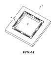
- FIGURE 4A is a top perspective view of the isolator 14.
- the isolator 14 includes the receptacle 17 and perimeter isolation tines 16.
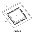
- FIGURE 4B illustrates an isolator 14' according to an embodiment of the present invention.
- the isolator 14' is used when the MEMS device and intended operating environment do not require a top cover 18, and thus does not have a receptacle 17.
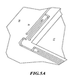
- FIGURE 5A is a partial top perspective view of the isolator of FIGURE 4 .
- the tines 16 can have a variety of flexural shapes.
- the tines 16 may have a single fold, more than one fold, or no folds.
- the tines 16 may be nested if desired, and may go around corners.
- the tines 16 may be formed by KOH etching, EDP, or TMAH.
- FIGURE 5B illustrates an alternate embodiment of the tines 16 that includes shock stops 15 to limit the amount of displacement allowed by the tines 16.
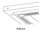
- FIGURE 6A is a partial bottom perspective view of the isolator 14 of FIGURE 2 .
- the isolator 14 includes the angled shelf 32 extending from the bottom side 28 of the isolator 14.
- the size, location, and angle of the shelf 32 may be varied to vary a vertical location of the die 22 with respect to the package 12.
- the shelf 32 can be used to raise the die 22 with respect to the package 12 when the vertical height of the die 22 and/or the vertical depth of the recess 19 require additional clearance between the bottom side 25 ( FIGURE 2 ) of the die 22 and the recess 19.
- the embodiment of the isolator 14 shown in FIGURE 6B , without a shelf 32, can be used.
- FIGURE 7 illustrates a process 40 according to the present invention.
- a MEMS device is attached to a first side of a die.
- a first side of an isolator is attached to the first side of the die.
- the first side of the isolator is attached to a package.
- the method 40 may include additional steps, such as etching isolation tines into the isolator, etching a receptacle into the isolator, and etching an angled shelf into the isolator.
- the method 40 may also include attaching a top cover to the die.
Landscapes
- Engineering & Computer Science (AREA)
- Microelectronics & Electronic Packaging (AREA)
- Computer Hardware Design (AREA)
- Micromachines (AREA)
- Pressure Sensors (AREA)
Claims (12)
- Dispositif (10) comprenant :un dispositif à systèmes microélectromécaniques (MEMS),une matrice (22) qui soutient le dispositif MEMS sur un premier côté de la matrice (22),un isolant (14) présentant un premier côté fixé au premier côté de la matrice (22), l'isolant comprenant des structures d'isolation (16), les structures d'isolation comprenant des tiges pointues formées dans l'épaisseur de l'isolant,un emballage (12) fixé au premier côté de l'isolant (14) etun dispositif de fixation (26) électriquement conducteur qui fixe la matrice (22) sur l'isolant (14) et qui fixe l'isolant (14) à l'emballage (12),les structures d'isolation (16) servant à réduire le niveau de contrainte exercé par l'emballage (12) sur la matrice (22).
- Dispositif (10) selon la revendication 1, comprenant en outre un recouvrement supérieur (18) fixé à la matrice (22).
- Dispositif (10) selon la revendication 2, dans lequel l'isolant (14) comprend en outre un réceptacle (17) formé dans l'épaisseur de l'isolant (14), le réceptacle (17) étant dimensionné et configuré pour permettre l'insertion du recouvrement supérieur (18) à travers le réceptacle (17).
- Dispositif (10) selon la revendication 1, dans lequel l'isolant (14) comprend en outre un plateau oblique prévu sur le premier côté de l'isolant (14).
- Dispositif (10) selon la revendication 1, dans lequel l'emballage (12) comprend un creux en gradins dimensionné et configuré pour loger l'isolant (14), la matrice (22) et le dispositif MEMS.
- Dispositif (10) selon la revendication 5, dans lequel l'emballage (12) comprend en outre un plateau (30) à fils, l'isolant (14) étant fixé sur le plateau (30) à fils.
- Dispositif (10) selon la revendication 4, dans lequel l'isolant (14) est fixé à l'emballage (12), une partie du plateau oblique étant en contact avec l'emballage (12).
- Dispositif (10) selon la revendication 1, dans lequel les tiges pointues comprennent des butées de choc (15).
- Procédé comprenant les étapes qui consistent à :fixer un dispositif MEMS sur un premier côté d'une matrice (22),fixer un premier côté d'un isolant (14) sur le premier côté de la matrice (22), l'isolant comprenant des structures d'isolation (16), les structures d'isolation comprenant des tiges pointues formées dans l'épaisseur de l'isolant etfixer le premier côté de l'isolant (14) à un emballage (12),les structures d'isolation (16) servant à réduire le niveau de contrainte exercé par l'emballage (12) sur la matrice (22).
- Procédé selon la revendication 8, dans lequel l'isolant comprend en outre un plateau oblique prévu sur le premier côté de l'isolant.
- Procédé selon la revendication 8, comprenant en outre la fixation d'un couvercle supérieur (18) à la matrice, l'isolant comprenant en outre un réceptacle (17) formé dans l'épaisseur de l'isolant, le réceptacle étant dimensionné et configuré pour permettre l'insertion du recouvrement supérieur par l'intermédiaire du réceptacle.
- Procédé selon la revendication 8, dans lequel les tiges pointues comprennent des butées de choc (15).
Applications Claiming Priority (1)
| Application Number | Priority Date | Filing Date | Title |
|---|---|---|---|
| US11/965,623 US7830003B2 (en) | 2007-12-27 | 2007-12-27 | Mechanical isolation for MEMS devices |
Publications (3)
| Publication Number | Publication Date |
|---|---|
| EP2075221A2 EP2075221A2 (fr) | 2009-07-01 |
| EP2075221A3 EP2075221A3 (fr) | 2013-05-29 |
| EP2075221B1 true EP2075221B1 (fr) | 2015-12-16 |
Family
ID=40379781
Family Applications (1)
| Application Number | Title | Priority Date | Filing Date |
|---|---|---|---|
| EP08171877.7A Ceased EP2075221B1 (fr) | 2007-12-27 | 2008-12-16 | Isolation mécanique pour dispositifs MEMS |
Country Status (3)
| Country | Link |
|---|---|
| US (1) | US7830003B2 (fr) |
| EP (1) | EP2075221B1 (fr) |
| JP (1) | JP5466400B2 (fr) |
Families Citing this family (34)
| Publication number | Priority date | Publication date | Assignee | Title |
|---|---|---|---|---|
| KR101443730B1 (ko) | 2010-09-18 | 2014-09-23 | 페어차일드 세미컨덕터 코포레이션 | 미세기계화 다이, 및 직교 오차가 작은 서스펜션을 제조하는 방법 |
| KR20130057485A (ko) | 2010-09-18 | 2013-05-31 | 페어차일드 세미컨덕터 코포레이션 | 미세 전자 기계 시스템에 미치는 응력을 감소시키기 위한 패키징 |
| EP2616389B1 (fr) | 2010-09-18 | 2017-04-05 | Fairchild Semiconductor Corporation | Boîtier de microsystème électromécanique à puces multiples |
| EP2616822B1 (fr) | 2010-09-18 | 2015-07-01 | Fairchild Semiconductor Corporation | Accéléromètre à 3 axes micro-usinés et à masse étalon unique |
| EP2616771B8 (fr) | 2010-09-18 | 2018-12-19 | Fairchild Semiconductor Corporation | Capteur inertiel monolithique 6 axes micro-usiné |
| US9278845B2 (en) | 2010-09-18 | 2016-03-08 | Fairchild Semiconductor Corporation | MEMS multi-axis gyroscope Z-axis electrode structure |
| KR101311966B1 (ko) | 2010-09-20 | 2013-10-14 | 페어차일드 세미컨덕터 코포레이션 | 감소된 션트 커패시턴스를 갖는 관통 실리콘 비아 |
| WO2012040211A2 (fr) | 2010-09-20 | 2012-03-29 | Fairchild Semiconductor Corporation | Capteur de pression micro-électromécanique comprenant un condensateur de référence |
| CN101920926B (zh) * | 2010-09-30 | 2012-11-28 | 无锡中微高科电子有限公司 | 一种不匹配封接应力释放结构 |
| US9062972B2 (en) | 2012-01-31 | 2015-06-23 | Fairchild Semiconductor Corporation | MEMS multi-axis accelerometer electrode structure |
| US8978475B2 (en) | 2012-02-01 | 2015-03-17 | Fairchild Semiconductor Corporation | MEMS proof mass with split z-axis portions |
| US9488693B2 (en) | 2012-04-04 | 2016-11-08 | Fairchild Semiconductor Corporation | Self test of MEMS accelerometer with ASICS integrated capacitors |
| US9069006B2 (en) | 2012-04-05 | 2015-06-30 | Fairchild Semiconductor Corporation | Self test of MEMS gyroscope with ASICs integrated capacitors |
| US20130264755A1 (en) * | 2012-04-05 | 2013-10-10 | Honeywell International Inc. | Methods and systems for limiting sensor motion |
| EP2647955B8 (fr) | 2012-04-05 | 2018-12-19 | Fairchild Semiconductor Corporation | Annulation du déphasage de quadrature de dispositif MEMS |
| EP2648334B1 (fr) | 2012-04-05 | 2020-06-10 | Fairchild Semiconductor Corporation | Amplificateur de charge frontal de dispositif MEMS |
| EP2647952B1 (fr) | 2012-04-05 | 2017-11-15 | Fairchild Semiconductor Corporation | Boucle de commande de gain automatique de dispositif MEMS pour entraînement d'amplitude mécanique |
| US9094027B2 (en) | 2012-04-12 | 2015-07-28 | Fairchild Semiconductor Corporation | Micro-electro-mechanical-system (MEMS) driver |
| US9625272B2 (en) | 2012-04-12 | 2017-04-18 | Fairchild Semiconductor Corporation | MEMS quadrature cancellation and signal demodulation |
| DE102013014881B4 (de) | 2012-09-12 | 2023-05-04 | Fairchild Semiconductor Corporation | Verbesserte Silizium-Durchkontaktierung mit einer Füllung aus mehreren Materialien |
| US8931765B2 (en) | 2012-09-27 | 2015-01-13 | Honeywell International Inc. | Systems and methods for high frequency isolation |
| EP2871456B1 (fr) | 2013-11-06 | 2018-10-10 | Invensense, Inc. | Capteur de pression et procédé de fabrication d'un capteur de pression |
| EP2871455B1 (fr) | 2013-11-06 | 2020-03-04 | Invensense, Inc. | Capteur de pression |
| DE102014210934A1 (de) * | 2014-06-06 | 2015-12-17 | Robert Bosch Gmbh | Vertikal hybrid integriertes MEMS-ASIC-Bauteil mit Stressentkopplungsstruktur |
| US10023461B2 (en) | 2014-10-31 | 2018-07-17 | Stmicroelectronics S.R.L. | Microintegrated encapsulated MEMS sensor with mechanical decoupling and manufacturing process thereof |
| EP3076146B1 (fr) | 2015-04-02 | 2020-05-06 | Invensense, Inc. | Capteur de pression |
| CN104950137B (zh) * | 2015-06-23 | 2018-01-19 | 西安电子科技大学 | 具有应力隔离结构的横向敏感加速度传感器芯片 |
| US10278281B1 (en) * | 2015-10-30 | 2019-04-30 | Garmin International, Inc. | MEMS stress isolation and stabilization system |
| EP3444609A1 (fr) | 2017-08-14 | 2019-02-20 | Sensirion AG | Mesurage de concentrations d'un gaz cible |
| US20190169018A1 (en) * | 2017-12-05 | 2019-06-06 | Invensense, Inc. | Stress isolation frame for a sensor |
| US11225409B2 (en) | 2018-09-17 | 2022-01-18 | Invensense, Inc. | Sensor with integrated heater |
| CN113785178B (zh) | 2019-05-17 | 2024-12-17 | 应美盛股份有限公司 | 气密性改进的压力传感器 |
| US11795052B2 (en) | 2020-09-29 | 2023-10-24 | Te Connectivity Solutions Gmbh | Constraint for a sensor assembly |
| GB2624843A (en) | 2022-07-08 | 2024-06-05 | Autorient Tech As | Micromechanical devices and methods of manufacturing thereof |
Family Cites Families (16)
| Publication number | Priority date | Publication date | Assignee | Title |
|---|---|---|---|---|
| US6714105B2 (en) * | 2002-04-26 | 2004-03-30 | Motorola, Inc. | Micro electro-mechanical system method |
| US20040041254A1 (en) * | 2002-09-04 | 2004-03-04 | Lewis Long | Packaged microchip |
| US6768196B2 (en) * | 2002-09-04 | 2004-07-27 | Analog Devices, Inc. | Packaged microchip with isolation |
| US6946742B2 (en) * | 2002-12-19 | 2005-09-20 | Analog Devices, Inc. | Packaged microchip with isolator having selected modulus of elasticity |
| US7166911B2 (en) * | 2002-09-04 | 2007-01-23 | Analog Devices, Inc. | Packaged microchip with premolded-type package |
| US20050189622A1 (en) * | 2004-03-01 | 2005-09-01 | Tessera, Inc. | Packaged acoustic and electromagnetic transducer chips |
| JP4815756B2 (ja) * | 2004-05-21 | 2011-11-16 | パナソニック株式会社 | アクチュエータ |
| JP4573695B2 (ja) * | 2005-04-27 | 2010-11-04 | 三洋電機株式会社 | マイクロマシンスイッチ |
| US7491567B2 (en) * | 2005-11-22 | 2009-02-17 | Honeywell International Inc. | MEMS device packaging methods |
| US20070114643A1 (en) * | 2005-11-22 | 2007-05-24 | Honeywell International Inc. | Mems flip-chip packaging |
| US8129801B2 (en) * | 2006-01-06 | 2012-03-06 | Honeywell International Inc. | Discrete stress isolator attachment structures for MEMS sensor packages |
| JP2007242462A (ja) * | 2006-03-09 | 2007-09-20 | Sanyo Electric Co Ltd | メカニカルスイッチ |
| US20070246665A1 (en) * | 2006-04-20 | 2007-10-25 | Lafond Peter H | Mechanical isolation for mems devices |
| US7280262B1 (en) * | 2006-05-24 | 2007-10-09 | Honeywell International Inc. | Integrated die level isolation for a MEMS device |
| US8742557B2 (en) | 2007-06-19 | 2014-06-03 | Honeywell International Inc. | Die mounting stress isolator |
| JP4851555B2 (ja) * | 2008-05-13 | 2012-01-11 | 株式会社デンソー | 力学量センサおよびその製造方法 |
-
2007
- 2007-12-27 US US11/965,623 patent/US7830003B2/en active Active
-
2008
- 2008-12-16 EP EP08171877.7A patent/EP2075221B1/fr not_active Ceased
- 2008-12-24 JP JP2008327692A patent/JP5466400B2/ja not_active Expired - Fee Related
Also Published As
| Publication number | Publication date |
|---|---|
| EP2075221A3 (fr) | 2013-05-29 |
| US20090166827A1 (en) | 2009-07-02 |
| US7830003B2 (en) | 2010-11-09 |
| JP2009154288A (ja) | 2009-07-16 |
| EP2075221A2 (fr) | 2009-07-01 |
| JP5466400B2 (ja) | 2014-04-09 |
Similar Documents
| Publication | Publication Date | Title |
|---|---|---|
| EP2075221B1 (fr) | Isolation mécanique pour dispositifs MEMS | |
| EP2616387B1 (fr) | Mise en boîtier permettant de réduire les contraintes sur des systèmes micro-électromécaniques | |
| US7615835B2 (en) | Package for semiconductor acceleration sensor | |
| US7268435B2 (en) | Capacitive semiconductor sensor | |
| EP3364165B1 (fr) | Capteur piezorésistif à flexibles de ressort pour l'isolement de contrainte | |
| US5394751A (en) | Method of producing semiconductor pressure sensor | |
| EP1886969A2 (fr) | Procédés pour la fabrication d'encapsulations sous vide de dispositifs sur wafer | |
| EP1129328A1 (fr) | Appareil integre et technique d'isolation des contraintes pour composants a semi-conducteur | |
| EP3141521B1 (fr) | Dispositif à capteur microélectromécanique avec une sensibilité au stress réduite et procédé de fabrication correspondant | |
| JP5990933B2 (ja) | 圧力センサパッケージの製造方法 | |
| EP3151271A1 (fr) | Dispositif encapsulé de matériau semi-conducteur présentant une sensibilité réduite aux contraintes thermo-mécaniques | |
| JP4754817B2 (ja) | 半導体加速度センサ | |
| EP2112489A2 (fr) | Capteur de pression, son procédé de fabrication et composant électronique correspondant | |
| US20070089511A1 (en) | Semiconductor device | |
| EP3260821B1 (fr) | Boîtier de capteur et procédé de fabrication du boîtier de capteur | |
| CN107892268B (zh) | 压力传感器及其制造方法 | |
| EP3452406B1 (fr) | Élément micromécanique de surface mécaniquement découplé et procédé pour sa fabrication | |
| EP2319798B1 (fr) | Encapsulation mems ayant des connexions électriques pour un montage sur tranche | |
| JPH09171033A (ja) | 加速度センサ | |
| CN105189337B (zh) | 微机电装置和制造方法 | |
| CN221283349U (zh) | Mems封装结构 | |
| CN114105084A (zh) | Mems共腔分膜的soc芯片及其制备方法 | |
| CN118641016A (zh) | 压电传感芯片、模组及振动检测装置 | |
| JPH05281250A (ja) | 多次元半導体加速度センサ | |
| JP2008249390A (ja) | 半導体装置及びその製造方法 |
Legal Events
| Date | Code | Title | Description |
|---|---|---|---|
| PUAI | Public reference made under article 153(3) epc to a published international application that has entered the european phase |
Free format text: ORIGINAL CODE: 0009012 |
|
| 17P | Request for examination filed |
Effective date: 20081216 |
|
| AK | Designated contracting states |
Kind code of ref document: A2 Designated state(s): AT BE BG CH CY CZ DE DK EE ES FI FR GB GR HR HU IE IS IT LI LT LU LV MC MT NL NO PL PT RO SE SI SK TR |
|
| AX | Request for extension of the european patent |
Extension state: AL BA MK RS |
|
| PUAL | Search report despatched |
Free format text: ORIGINAL CODE: 0009013 |
|
| AK | Designated contracting states |
Kind code of ref document: A3 Designated state(s): AT BE BG CH CY CZ DE DK EE ES FI FR GB GR HR HU IE IS IT LI LT LU LV MC MT NL NO PL PT RO SE SI SK TR |
|
| AX | Request for extension of the european patent |
Extension state: AL BA MK RS |
|
| RIC1 | Information provided on ipc code assigned before grant |
Ipc: B81B 7/00 20060101AFI20130425BHEP |
|
| AKX | Designation fees paid |
Designated state(s): FR |
|
| REG | Reference to a national code |
Ref country code: DE Ref legal event code: R108 |
|
| 17Q | First examination report despatched |
Effective date: 20140116 |
|
| REG | Reference to a national code |
Ref country code: DE Ref legal event code: R108 Effective date: 20140205 |
|
| GRAP | Despatch of communication of intention to grant a patent |
Free format text: ORIGINAL CODE: EPIDOSNIGR1 |
|
| INTG | Intention to grant announced |
Effective date: 20150915 |
|
| RIN1 | Information on inventor provided before grant (corrected) |
Inventor name: JAFRI, IJAZ Inventor name: FOSTER, MICHAEL Inventor name: ZHOU, SHIFANG Inventor name: ESKRIDGE, MARK |
|
| GRAS | Grant fee paid |
Free format text: ORIGINAL CODE: EPIDOSNIGR3 |
|
| GRAA | (expected) grant |
Free format text: ORIGINAL CODE: 0009210 |
|
| AK | Designated contracting states |
Kind code of ref document: B1 Designated state(s): FR |
|
| RAP1 | Party data changed (applicant data changed or rights of an application transferred) |
Owner name: HONEYWELL INTERNATIONAL INC. |
|
| REG | Reference to a national code |
Ref country code: FR Ref legal event code: PLFP Year of fee payment: 8 |
|
| PLBE | No opposition filed within time limit |
Free format text: ORIGINAL CODE: 0009261 |
|
| STAA | Information on the status of an ep patent application or granted ep patent |
Free format text: STATUS: NO OPPOSITION FILED WITHIN TIME LIMIT |
|
| REG | Reference to a national code |
Ref country code: FR Ref legal event code: PLFP Year of fee payment: 9 |
|
| 26N | No opposition filed |
Effective date: 20160919 |
|
| REG | Reference to a national code |
Ref country code: FR Ref legal event code: PLFP Year of fee payment: 10 |
|
| PGFP | Annual fee paid to national office [announced via postgrant information from national office to epo] |
Ref country code: FR Payment date: 20191224 Year of fee payment: 12 |
|
| PG25 | Lapsed in a contracting state [announced via postgrant information from national office to epo] |
Ref country code: FR Free format text: LAPSE BECAUSE OF NON-PAYMENT OF DUE FEES Effective date: 20201231 |
|
| P01 | Opt-out of the competence of the unified patent court (upc) registered |
Effective date: 20230525 |