EP2075233A2 - Ensemble de tige en germe de silicium polycristallin, son procédé de fabrication, appareil de fabrication de silicium polycristallin et procédé de fabrication de silicium polycristallin - Google Patents
Ensemble de tige en germe de silicium polycristallin, son procédé de fabrication, appareil de fabrication de silicium polycristallin et procédé de fabrication de silicium polycristallin Download PDFInfo
- Publication number
- EP2075233A2 EP2075233A2 EP08172840A EP08172840A EP2075233A2 EP 2075233 A2 EP2075233 A2 EP 2075233A2 EP 08172840 A EP08172840 A EP 08172840A EP 08172840 A EP08172840 A EP 08172840A EP 2075233 A2 EP2075233 A2 EP 2075233A2
- Authority
- EP
- European Patent Office
- Prior art keywords
- silicon seed
- silicon
- connection member
- seed rod
- end portion
- Prior art date
- Legal status (The legal status is an assumption and is not a legal conclusion. Google has not performed a legal analysis and makes no representation as to the accuracy of the status listed.)
- Granted
Links
Images


Classifications
-
- C—CHEMISTRY; METALLURGY
- C23—COATING METALLIC MATERIAL; COATING MATERIAL WITH METALLIC MATERIAL; CHEMICAL SURFACE TREATMENT; DIFFUSION TREATMENT OF METALLIC MATERIAL; COATING BY VACUUM EVAPORATION, BY SPUTTERING, BY ION IMPLANTATION OR BY CHEMICAL VAPOUR DEPOSITION, IN GENERAL; INHIBITING CORROSION OF METALLIC MATERIAL OR INCRUSTATION IN GENERAL
- C23C—COATING METALLIC MATERIAL; COATING MATERIAL WITH METALLIC MATERIAL; SURFACE TREATMENT OF METALLIC MATERIAL BY DIFFUSION INTO THE SURFACE, BY CHEMICAL CONVERSION OR SUBSTITUTION; COATING BY VACUUM EVAPORATION, BY SPUTTERING, BY ION IMPLANTATION OR BY CHEMICAL VAPOUR DEPOSITION, IN GENERAL
- C23C16/00—Chemical coating by decomposition of gaseous compounds, without leaving reaction products of surface material in the coating, i.e. chemical vapour deposition [CVD] processes
- C23C16/02—Pretreatment of the material to be coated
-
- C—CHEMISTRY; METALLURGY
- C01—INORGANIC CHEMISTRY
- C01B—NON-METALLIC ELEMENTS; COMPOUNDS THEREOF; METALLOIDS OR COMPOUNDS THEREOF NOT COVERED BY SUBCLASS C01C
- C01B33/00—Silicon; Compounds thereof
- C01B33/02—Silicon
- C01B33/021—Preparation
- C01B33/027—Preparation by decomposition or reduction of gaseous or vaporised silicon compounds other than silica or silica-containing material
- C01B33/035—Preparation by decomposition or reduction of gaseous or vaporised silicon compounds other than silica or silica-containing material by decomposition or reduction of gaseous or vaporised silicon compounds in the presence of heated filaments of silicon, carbon or a refractory metal, e.g. tantalum or tungsten, or in the presence of heated silicon rods on which the formed silicon is deposited, a silicon rod being obtained, e.g. Siemens process
-
- C—CHEMISTRY; METALLURGY
- C23—COATING METALLIC MATERIAL; COATING MATERIAL WITH METALLIC MATERIAL; CHEMICAL SURFACE TREATMENT; DIFFUSION TREATMENT OF METALLIC MATERIAL; COATING BY VACUUM EVAPORATION, BY SPUTTERING, BY ION IMPLANTATION OR BY CHEMICAL VAPOUR DEPOSITION, IN GENERAL; INHIBITING CORROSION OF METALLIC MATERIAL OR INCRUSTATION IN GENERAL
- C23C—COATING METALLIC MATERIAL; COATING MATERIAL WITH METALLIC MATERIAL; SURFACE TREATMENT OF METALLIC MATERIAL BY DIFFUSION INTO THE SURFACE, BY CHEMICAL CONVERSION OR SUBSTITUTION; COATING BY VACUUM EVAPORATION, BY SPUTTERING, BY ION IMPLANTATION OR BY CHEMICAL VAPOUR DEPOSITION, IN GENERAL
- C23C16/00—Chemical coating by decomposition of gaseous compounds, without leaving reaction products of surface material in the coating, i.e. chemical vapour deposition [CVD] processes
- C23C16/22—Chemical coating by decomposition of gaseous compounds, without leaving reaction products of surface material in the coating, i.e. chemical vapour deposition [CVD] processes characterised by the deposition of inorganic material, other than metallic material
- C23C16/24—Deposition of silicon only
-
- Y—GENERAL TAGGING OF NEW TECHNOLOGICAL DEVELOPMENTS; GENERAL TAGGING OF CROSS-SECTIONAL TECHNOLOGIES SPANNING OVER SEVERAL SECTIONS OF THE IPC; TECHNICAL SUBJECTS COVERED BY FORMER USPC CROSS-REFERENCE ART COLLECTIONS [XRACs] AND DIGESTS
- Y10—TECHNICAL SUBJECTS COVERED BY FORMER USPC
- Y10T—TECHNICAL SUBJECTS COVERED BY FORMER US CLASSIFICATION
- Y10T117/00—Single-crystal, oriented-crystal, and epitaxy growth processes; non-coating apparatus therefor
- Y10T117/10—Apparatus
-
- Y—GENERAL TAGGING OF NEW TECHNOLOGICAL DEVELOPMENTS; GENERAL TAGGING OF CROSS-SECTIONAL TECHNOLOGIES SPANNING OVER SEVERAL SECTIONS OF THE IPC; TECHNICAL SUBJECTS COVERED BY FORMER USPC CROSS-REFERENCE ART COLLECTIONS [XRACs] AND DIGESTS
- Y10—TECHNICAL SUBJECTS COVERED BY FORMER USPC
- Y10T—TECHNICAL SUBJECTS COVERED BY FORMER US CLASSIFICATION
- Y10T29/00—Metal working
- Y10T29/49—Method of mechanical manufacture
- Y10T29/49826—Assembling or joining
Definitions
- the present invention relates to a silicon seed rod assembly used for producing polycrystalline silicon in a polycrystalline silicon reaction furnace, and a method of forming the same. Further, the present invention relates to a polycrystalline silicon producing apparatus employing the silicon seed rod assembly and a method of producing polycrystalline silicon.
- a silicon seed rod assembly used for producing polycrystalline silicon in a polycrystalline silicon reaction furnace
- a polycrystalline silicon producing apparatus employing the silicon seed rod assembly and a method of producing polycrystalline silicon.
- the Siemens method is known as a method of producing high-purity polycrystalline silicon used as a semiconductor material.
- the Siemens method is a method of making raw gas composed of mixed gas of chlorosilane and hydrogen to contact with a heated silicon seed rod assembly and of making polycrystalline silicon deposited on a surface of the silicon seed rod assembly by means of a reaction of the raw gas.
- a polycrystalline silicon reaction furnace is used in which a plurality of silicon seed rod assemblies is uprightly provided in a hermetic reaction furnace (see Japanese Patent No. 3819252 and Japanese Patent No. 3881647 ).
- Each silicon seed rod assembly includes two rod-shaped silicon seed rods and a connection member connecting the upper end portions of the silicon seed rods to each other, thereby forming the silicon seed rod assembly in a ⁇ -shape. Then, the lower end portion of the silicon seed rod is fixed to an electrode provided in a bottom of the polycrystalline silicon reaction furnace. The silicon seed rod assembly is heated by supplying current from the electrode at the lower end portion thereof. Then, the raw gas is thermally decomposed or is reduced with hydrogen by joule heat produced at this time, thereby making polycrystalline silicon deposited on the surface of the silicon seed rod assembly.
- a section of the rod-shaped silicon seed rod is formed in a square shape, a circular shape, or a shape in which angular portions of a square shape are R-chamfered.
- the upper end portion connected to the connection member is formed in a cylindrical shape so as to have a diameter slightly smaller than that of the through-hole.
- a step portion is formed between an upper end portion and a main body portion of the silicon seed rod since a width of the upper end portion is smaller than that of the main body portion.
- the step portion is provided with a flat support surface disposed in a direction perpendicular to a longitudinal direction of the silicon seed rod. Then, the upper end portions of the two silicon seed rods are inserted through the through-holes formed in both end portions of the connection member, and the support surface supports an opening-end peripheral edge of the through-hole on the side of the lower surface of the connection member, thereby forming the silicon seed rod assembly.
- the through-hole is formed by perforating the connection member by means of a drill from the one side surface toward the other side surface thereof.
- a petal-shape defect portion may be formed in the opening-end peripheral edge on the side of the other side surface in a perforation direction due to brittleness of the connection member.
- the silicon seed rod assembly is formed so that the other side surface having the defect portion formed thereon comes into contact with the support surface, a contact area between the connection member and the silicon seed rod decreases.
- the present invention is contrived in consideration of the above-described circumstances, and an object of the invention is to provide a silicon seed rod assembly capable of satisfactorily ensuring a contact area between a silicon seed rod and a connection member and of producing polycrystalline silicon through a reliable process, and a method of forming the silicon seed rod assembly. Further, an object of the invention is to provide a polycrystalline silicon producing apparatus using the silicon seed rod assembly and a method of producing polycrystalline silicon.
- the present invention adopts the following configuration. That is, according to an aspect of the invention, there is disclosed a silicon seed rod assembly used for producing polycrystalline silicon by means of a vapor deposition method, the silicon seed rod assembly including: two rod-shaped silicon seed rods; and a silicon connection member bridging the silicon seed rods, wherein a width of an upper end portion of each silicon seed rod is smaller than that of a main body portion thereof, wherein a step portion formed between the upper end portion and the main body portion is provided with a support surface disposed in a direction perpendicular to a longitudinal direction of the upper end portion, wherein the connection member is provided with a through-hole into which the upper end portion is inserted, wherein an opening-end peripheral edge of the through-hole on one side surface of the connection member is sharper than that on the other side surface thereof, and an opening-end peripheral surface on the one side surface thereof is formed into a flat contact surface disposed in a direction perpendicular to a perforation direction of
- a method of forming a silicon seed rod assembly which is used for producing polycrystalline silicon by means of a vapor deposition method and includes two rod-shaped silicon seed rods and a silicon connection member bridging the silicon seed rods, the method including the steps of: forming an upper end portion, of which a width is smaller than that of a main body portion, at an upper end of each silicon seed rod; forming a support surface at a step portion between the upper end portion and the main body portion so as to be disposed in a direction perpendicular to a longitudinal direction of the upper end portion; forming a through-hole by perforating the connection member from one side surface thereof by means of a drill in a direction perpendicular to the one side surface; and inserting the upper end portion into the through-hole so that the one side surface comes into contact with the support surface of the silicon seed rod.
- the opening-end peripheral edge of the through-hole on one side surface of the connection member is sharper than that on the other side surface thereof, the opening-end peripheral surface on the one side surface thereof is formed into the flat contact surface, the support surface of the silicon seed rod comes into contact with the contact surface, and then the connection member is supported by the two silicon seed rods, thereby forming the silicon seed rod assembly. Accordingly, since it is possible to satisfactorily ensure the contact area between the silicon seed rod and the connection member, it is possible to restrict an increase in the contact resistance therebetween and to prevent the meltdown of the contact portion caused by overheating during an ohmic heating.
- connection member may include an inclined surface of which a width gradually decreases from the downside to the upside. Accordingly, the connection member is formed in a shape in which silica or foreign material flowing from the above of the connection member is hardly collected or attached thereto upon producing the polycrystalline silicon, thereby producing highly pure polycrystalline silicon.
- a polycrystalline silicon producing apparatus including: the silicon seed rod assembly according to the above-described aspect provided in a reaction furnace, wherein at least a pair of electrodes is provided in a bottom portion in the reaction furnace, and end portions, disposed on the opposite side of the connection member, of both silicon seed rods of the silicon seed rod assembly are supported by the electrodes, respectively. Since local overheating of the silicon seed rod assembly is prevented, it is possible to reliably produce polycrystalline silicon.
- a method of producing polycrystalline silicon including the steps of: forming a silicon seed rod assembly by uprightly supporting silicon seed rods by a pair of electrodes, respectively, disposed in a bottom portion in a reaction furnace and by providing a silicon connection member between upper end portions of the silicon seed rods; heating the silicon seed rods by supplying current to the electrodes; reacting the raw gas supplied to the reaction furnace; and depositing polycrystalline silicon on surfaces of the silicon seed rods, wherein the step of forming the silicon seed rod assembly includes the steps of: forming an upper end portion, of which a width is smaller than that of a main body portion, at an upper end of each silicon seed rod and forming a support surface at a step portion between the upper end portion and the main body portion so as to be disposed in a direction perpendicular to a longitudinal direction of the upper end portion; forming a through-hole by perforating the connection member from one side surface thereof by means of a drill in a direction perpendicular to the one
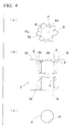
- a polycrystalline silicon producing apparatus includes a polycrystalline silicon reaction furnace 10.
- the polycrystalline silicon reaction furnace 10 is provided with a bell jar 12 formed in a bell shape so as to cover the whole upper portion of a round furnace bottom 11, and the inside of the polycrystalline silicon reaction furnace 10 is sealed by the furnace bottom 11 and the bell jar 12.
- the sealed inside portion is provided with a plurality of upright silicon seed rod assemblies 1 which is formed in a substantially 11-shape and of which the upper end portions are connected to each other, where both base end portions of each silicon seed rod assembly 1 are supported by electrodes 13 formed in the furnace bottom 11.
- the furnace bottom I 1 is provided with a plurality of raw gas supply ports 14 for supplying raw gas containing trichlorosilane and hydrogen toward the silicon seed rod assembly 1 provided inside the polycrystalline silicon reaction furnace 10.
- the raw gas supply ports 14 are arranged at an appropriate interval therebetween so as to uniformly supply the raw gas to the plurality of silicon seed rod assemblies 1.
- the raw gas supply ports 14 are connected to a raw gas supply pipe line 15, and the raw gas supply pipe line 15 is connected to a raw gas supply source 17 via a flow rate control valve 16. Accordingly, the raw gas of which the flow rate is controlled by the flow rate control valve 16 is supplied to the raw gas supply ports 14 via the raw gas supply pipe line 15 to be thereby supplied to the inside of the polycrystalline silicon reaction furnace 10. Additionally, the furnace bottom 11 is provided with a plurality of discharge ports 18 for discharging gas obtained by a reaction of the raw gases. Also, the discharge ports 18 are arranged at the appropriate intervals therebetween so as to uniformly discharge the reacted gas, and are connected to an exhaust gas processing system 19 in the outside of the reaction furnace 10.
- the silicon seed rod assembly 1 includes two silicon seed rods 2 which are arranged in parallel to each other and are formed in an angular-rod shape, and a connection member 3 which is provided in the upper end portions of the silicon seed rods 2 and is formed in an angular-rod shape or a flat-plate shape, the silicon seed rod assembly 1 being formed in a n-shape or a inverted U-shape as a whole.
- Each silicon seed rod 2 is formed by cutting a polycrystalline silicon rod produced in advance, where the longitudinal upper end portion is formed in a cylindrical shape having a diameter smaller than that of a main body portion 2A and the upper end portion is an upper end portion 2B.
- a step portion located between the upper end portion 2B and the main body portion 2A of the silicon seed rod 2 is provided with a flat surface disposed in a direction perpendicular to a longitudinal direction of upper end portion 2B, and the flat surface is a support surface 2C.
- the silicon seed rod assembly 1 is provided with through-holes 4 which are formed in both longitudinal end portions of the connection member 3 so as to be formed through an upper surface 3A and a lower surface 3B of the connection member 3 and to make the upper end portions 2B of the silicon seed rods 2 to be inserted therethrough, respectively.
- Each through-hole 4 is formed in a cylindrical-hole shape having an inner diameter larger than a width of the upper end portion 2B of the silicon seed rod 2. Additionally, a length of the through-hole 4 is approximately the same as that of the upper end portion 2B or is shorter than the upper end portion 2B, and the through-hole 4 is formed in advance by a drill.
- FIG. 2 shows a state where the upper end portion 2B protrudes from the connection member 3. Additionally, upon forming the through-hole 4, a direction in which the drill perforates the connection member 3 corresponds to a direction from the lower surface (a surface on one side) 3B to the upper surface (a surface on the other side) 3A in FIG. 2 .
- the defect portion 4A is formed in the opening-end peripheral edge of the through-hole 4 formed in the upper surface 3A of the connection member 3. Accordingly, as shown in FIG. 4 (a) and (b) , at least a part of a ridge line Ro, in which the upper surface 3A of the connection member 3 intersects the inner-peripheral surface of the through-hole 4 and which is necessary to be formed in a circular shape, is missed at the defect portion 4A.
- the opening-end peripheral edge is widened and curved toward the outside of the through-hole 4 in a radial direction by a defect portion ridge line S in which the surface of the defect portion 4A intersects the upper surface 3A of the connection member 3.
- the opening-end peripheral edge of the through-hole 4 formed in the lower surface 3B on the rear end side in a perforation direction of the drill is not provided with the defect portion 4A increasing contact resistance. That is, as shown in FIG. 4 (b) and (c) , the opening-end peripheral edge of the through-hole 4 formed in the lower surface 3B is formed in a sharp circular shape, that is, a so-called sharp edge shape by a ridge line R in which the flat lower surface 3B intersects the inner-peripheral surface of the through-hole 4 and which is continuous in a circumferential direction.
- the lower surface 3B is formed into a flat surface disposed in a direction perpendicular to a perforation direction of the through-hole 4, and an opening-end peripheral surface is formed into a contact surface 3C.
- the upper end portions 2B of the two silicon seed rods 2 are inserted into the through-holes 4 formed in both end portions of the connection member 3 in a direction from the lower surface 3B to the upside, respectively, and the support surface 2C of the silicon seed rod 2 comes into contact with the contact surface 3C of the connection member 3, thereby enabling the silicon seed rods 2 to support the connection member 3. Accordingly, it is possible to satisfactorily ensure a contact area between the support surface 2C and the contact surface 3C without the defect portion 4A.
- an inner diameter of the through-hole 4 is in the range of 5 to 8 mm.
- a length A in a radial direction of the through-hole 4 formed in the upper surface 3A of the connection member 3 is 3 mm or less, and a depth B in a longitudinal direction of the through-hole 4 is 2 mm or less, which are allowable ranges thereof.
- a width W of the connection member 3 is set to be equal to or larger than a maximum width C of the main body portion 2A of the silicon seed rod 2 (in the case of the main body portion 2A configured as an angular rod as shown in FIG. 3 , a diagonal dimension of the section).
- a distance H from the center of the through-hole 4 to the front end portion of the connection member 3 is set to be equal to or larger than a half of the maximum width C of the main body portion 2A of the silicon seed rod 2.
- the whole surface of the support surface 2C is configured to be brought into contact with the contact surface 3C of the connection member 3 regardless of a rotary direction about a shaft center of the silicon seed rod 2.
- the through-hole 4 of the connection member 3 is formed in a direction perpendicular to the contact surface 3C, and the upper end portion 2B of the silicon seed rod 2 is formed in a direction perpendicular to the support surface 2C.
- the opening-end peripheral edge of the through-hole 4 formed in the lower surface 3B is formed by the sharp (sharp-edge) circular ridge line R, and an opening-end peripheral surface is formed into the flat contact surface 3C.
- the flat support surface 2C of the silicon seed rod 2 comes into contact with the contact surface 3C, and the connection member 3 is supported by the two silicon seed rods 2, thereby forming the silicon seed rod assembly 1.
- connection member 3 is formed in the angular-rod shape
- shape is not limited thereto, but may be formed in a shape according to a first modified example shown in FIG. 5 .
- components different from the above-described embodiment will be mainly described.
- the same reference numerals are given to the same components, and the description thereof will be omitted.
- a side surface 21D of a connection member 21 is formed into an inclined surface, and a section in a direction perpendicular to a longitudinal direction thereof is formed in a triangular shape.
- the opening-end peripheral edge is formed by the sharp (sharp-edge) ridge line R without forming the defect portion 4A in the opening-end peripheral edge of the through-hole 4 formed in the lower surface 3B of the connection member 21.
- the flat contact surface 3C is formed in the periphery of the opening end in a direction perpendicular to a perforation direction of the through-hole 4.
- the upper end portions 2B of the two silicon seed rods 2 are inserted into the through-holes 4 formed in both end portions of the connection member 21 in a direction from the lower surface 3B to the upside, respectively, and the flat support surface 2C of the silicon seed rod 2 comes into contact with the contact surface 3C of the connection member 21 so as to support the connection member 21 by means of the two silicon seed rods 2, thereby forming the silicon seed rod assembly 22. Accordingly, it is possible to satisfactorily ensure a contact area between the silicon seed rod 2 and the connection member 21 and to prevent the meltdown of the contact portion caused by overheating during an ohmic heating.
- connection member 21 is formed into an inclined surface by gradually decreasing a horizontal width thereof in an upward direction, silica or foreign material flowing from the above of the connection member 21 is hardly collected or attached thereto upon producing the polycrystalline silicon, thereby producing highly pure polycrystalline silicon.
- connection member is not limited to the angular shape or the triangular shape described above, but may be different shapes so long as the opening-end peripheral edge of the through-hole is formed by the sharp (sharp-edge) ridge line R, the flat contact surface 3C is formed in periphery of the opening end in a direction perpendicular to a perforation direction of the through-hole 4, and the contact area between the contact surface 3C and the support surface 2C is satisfactorily ensured. It is desirable to form the side surface 21D of the connection member 21 into an inclined surface since it is possible to form the highly pure polycrystalline silicon on the grounds of the above-described reason.
- a through-hole 27 formed through a connection member 26 may be formed in a substantially conical shape of which a head portion is cut out by gradually decreasing a diameter thereof in a direction from the lower surface 3B to the upper surface 3A of the connection member 26, the flat contact surface 3C may be provided in a direction perpendicular to a perforation direction of the through-hole 27, and then an upper end portion 28B of a silicon seed rod 28 may be formed in a substantially conical shape of which a head portion is cut out so as to match with the shape of the through-hole 27.
- a special drill is prepared in advance of which the front end portion is formed to have an acute angle, a perforation depth is determined by means of a jig or the like, and then the drilling is carried out in a direction from the lower surface 3B to the upper surface 3A. Accordingly, the defect portion 4A is formed in the upper surface 3A of the connection member 26, but the opening-end peripheral edge of the lower surface 3B of the connection member 26 is formed by the sharp ridge line R.
- an angle D formed between the upper surface 3A of the connection member 26 and the inner-peripheral surface of the through-hole 27 is desirably in the range of 45° to 80°, and more desirably in the range of 75° to 80°.
- the through-hole 27 of the connection member 26 and the upper end portion 28B of the silicon seed rod 28 is made to be brought into contact with each other with large area, it is possible to more reliably ensure the contact area and to prevent the meltdown during an ohmic heating.
- the angle D formed between the upper surface 3A of the connection member 26 and the inner-peripheral surface of the through-hole 27 according to the second modified example shown in FIG. 6 is different from that according to the third modified example shown in FIG 7 , the same reference numeral is used in both drawings.
- the silicon seed rod is formed in the angular-rod shape
- the shape is not limited thereto, but the section of the rod-shape silicon seed rod may be formed in a polygonal shape instead of a square shape.
- the section of the rod-shape silicon seed rod may be formed in a shape in which angular portions are chamfered into a flat surface (C-chamfered) or are chamfered into a circular-arc surface (R-chamfered), or may be formed in a circular shape or an oval shape.
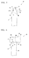
- both silicon seed rods are uprightly provided, both silicon seed rods may be provided while being inclined with respect to a perpendicular direction and may be connected to each other in a bent state by means of the connection member as shown in FIG. 8 .
- both silicon seed rods 2 are supported in an inclined state so as to be gradually distanced from each other in a direction from the base end portion to the upper end portion 2B.
- a gap L 1 between the upper end portions 2B of the pair of silicon seed rods 2 is wider than a gap L 2 between the pair of through-holes 4 formed in the connection member 3.
- the gap L 2 between both through-holes 4 formed in the connection member 3 is set to be equal to a gap L 3 between seed rod supporting portions of both electrodes 13 by which the silicon seed rod assembly 1 is supported.
- the defect portion 4A may be formed in the opening-end peripheral edge of the upper surface 3A of the connection member 3, but the opening-end peripheral edge of the lower surface 3B of the connection member 3 is formed by the sharp ridge line R in which the inner-peripheral surface of the through-hole 27 intersects the lower surface 3B. Then, as shown in FIG.
- both silicon seed rods 2 are bent so as to make the upper end portions 2B thereof to be close to each other, and then the upper end portions 2B are inserted into the through-holes 4 of the connection member 3, respectively.
- a stretching force caused by a restoring force acts on the connection member 3 in a direction in which both through-holes 4 are separated from each other as depicted by arrows shown in FIG 9 .
- the circular-arc surface on the outer side in a separation direction (designated by arrows in FIG.
- both silicon seed rods are not formed in the linear shape and are bent, both silicon seed rods may be arranged so as to be gradually distanced from each other in a direction from the base end portion to the upper end portion due to the bending thereof, and may be connected to each other by decreasing the distance between the upper end portions.
- the silicon seed rods may be uprightly provided in a state where a gap between the upper end portions of the silicon seed rods is narrower than a gap between the through-holes of the connection member, and may be inserted into both through-holes of the connection member by widening the gap between the upper end portions of the silicon seed rods.
- a gap between the silicon seed rod supporting portions of the electrodes may be set to be different from a gap between the through-holes of the connection member, the silicon seed rods may be uprightly provided in the electrodes in a perpendicular direction, and then the upper end portions of the silicon seed rods may be connected to each other by means of the connection member by bending the silicon seed rods.
- an angle formed between the contact surface and the through-hole of the connection member is equal to an angle formed between the support surface and the upper end portion of the silicon seed rod, and the contact surface of the connection member makes contact with the support surface of the silicon seed rod in a state where the upper end portion of the silicon seed rod is inserted into the through-hole of the connection member.
- the angle is desirably 90°. While preferred embodiments of the invention have been described and illustrated above, it should be understood that these are exemplary of the invention and are not to be considered as limiting. Additions, omissions, substitutions, and other modifications can be made without departing from the spirit or scope of the present invention. Accordingly, the invention is not to be considered as being limited by the foregoing description, and is only limited by the scope of the appended claims.
Landscapes
- Chemical & Material Sciences (AREA)
- Organic Chemistry (AREA)
- Inorganic Chemistry (AREA)
- General Chemical & Material Sciences (AREA)
- Chemical Kinetics & Catalysis (AREA)
- Engineering & Computer Science (AREA)
- Materials Engineering (AREA)
- Mechanical Engineering (AREA)
- Metallurgy (AREA)
- Silicon Compounds (AREA)
Applications Claiming Priority (1)
| Application Number | Priority Date | Filing Date | Title |
|---|---|---|---|
| JP2007338409 | 2007-12-28 |
Publications (3)
| Publication Number | Publication Date |
|---|---|
| EP2075233A2 true EP2075233A2 (fr) | 2009-07-01 |
| EP2075233A3 EP2075233A3 (fr) | 2009-07-29 |
| EP2075233B1 EP2075233B1 (fr) | 2014-06-18 |
Family
ID=40535577
Family Applications (1)
| Application Number | Title | Priority Date | Filing Date |
|---|---|---|---|
| EP08172840.4A Active EP2075233B1 (fr) | 2007-12-28 | 2008-12-23 | Ensemble de tiges en germe de silicium polycristallin, son procédé de fabrication, appareil de fabrication de silicium polycristallin et procédé de fabrication de silicium polycristallin |
Country Status (5)
| Country | Link |
|---|---|
| US (2) | US20090165704A1 (fr) |
| EP (1) | EP2075233B1 (fr) |
| JP (1) | JP5309963B2 (fr) |
| KR (1) | KR101529732B1 (fr) |
| CN (1) | CN101469447B (fr) |
Cited By (2)
| Publication number | Priority date | Publication date | Assignee | Title |
|---|---|---|---|---|
| EP2077252A3 (fr) * | 2007-11-28 | 2011-03-02 | Mitsubishi Materials Corporation | Appareil de fabrication de silicium polycristallin et procédé de fabrication |
| WO2015014747A1 (fr) * | 2013-08-01 | 2015-02-05 | Wacker Chemie Ag | Corps de support pour le dépôt de silicium polycristallin |
Families Citing this family (6)
| Publication number | Priority date | Publication date | Assignee | Title |
|---|---|---|---|---|
| CN101775643B (zh) * | 2009-12-23 | 2012-06-13 | 洛阳金诺机械工程有限公司 | 一种整体“u”形硅芯的生产工艺 |
| JP2012224499A (ja) * | 2011-04-19 | 2012-11-15 | Shin-Etsu Chemical Co Ltd | シリコン芯線の製造方法 |
| KR101339481B1 (ko) * | 2011-08-05 | 2013-12-10 | 주식회사 글로실 | 단결정 실리콘 웨이퍼 원료 제조를 위한 다결정 실리콘 로드 제조방법 |
| US9701541B2 (en) * | 2012-12-19 | 2017-07-11 | Gtat Corporation | Methods and systems for stabilizing filaments in a chemical vapor deposition reactor |
| DE102013206339A1 (de) * | 2013-04-10 | 2014-10-16 | Wacker Chemie Ag | Vorrichtung und Verfahren zum Ausbau von polykristallinen Siliciumstäben aus einem Reaktor |
| WO2017087293A1 (fr) * | 2015-11-16 | 2017-05-26 | Gtat Corporation | Procédé et appareil de dépôt chimique en phase vapeur |
Citations (2)
| Publication number | Priority date | Publication date | Assignee | Title |
|---|---|---|---|---|
| JP3819252B2 (ja) | 2001-05-21 | 2006-09-06 | 住友チタニウム株式会社 | シード保持電極 |
| JP3881647B2 (ja) | 2003-10-07 | 2007-02-14 | 住友チタニウム株式会社 | 多結晶シリコンロッド及びその製造方法 |
Family Cites Families (10)
| Publication number | Priority date | Publication date | Assignee | Title |
|---|---|---|---|---|
| US2763581A (en) * | 1952-11-25 | 1956-09-18 | Raytheon Mfg Co | Process of making p-n junction crystals |
| US3011877A (en) * | 1956-06-25 | 1961-12-05 | Siemens Ag | Production of high-purity semiconductor materials for electrical purposes |
| DE1155759B (de) * | 1959-06-11 | 1963-10-17 | Siemens Ag | Vorrichtung zur Gewinnung reinsten kristallinen Halbleitermaterials fuer elektrotechnische Zwecke |
| DE2050076C3 (de) * | 1970-10-12 | 1980-06-26 | Siemens Ag, 1000 Berlin Und 8000 Muenchen | Vorrichtung zum Herstellen von Rohren aus Halbleitermaterial |
| DE2149526C3 (de) * | 1970-10-12 | 1980-09-25 | Siemens Ag, 1000 Berlin Und 8000 Muenchen | Vorrichtung zum Herstellen von Rohren aus Silicium |
| US3820935A (en) * | 1971-10-04 | 1974-06-28 | Siemens Ag | Method and device for the production of tubular members of silicon |
| US5304417A (en) * | 1989-06-02 | 1994-04-19 | Air Products And Chemicals, Inc. | Graphite/carbon articles for elevated temperature service and method of manufacture |
| JPH0729874B2 (ja) * | 1989-11-04 | 1995-04-05 | コマツ電子金属株式会社 | 多結晶シリコン製造装置の芯線間接続用ブリッジ |
| JP4941631B2 (ja) * | 2005-11-21 | 2012-05-30 | 三菱マテリアル株式会社 | シリコンシードおよびその製造方法 |
| JP2009062251A (ja) * | 2007-09-10 | 2009-03-26 | Mitsubishi Materials Corp | 多結晶シリコンの製造装置及び製造方法 |
-
2008
- 2008-12-19 JP JP2008323585A patent/JP5309963B2/ja active Active
- 2008-12-23 US US12/318,270 patent/US20090165704A1/en not_active Abandoned
- 2008-12-23 EP EP08172840.4A patent/EP2075233B1/fr active Active
- 2008-12-24 KR KR1020080133699A patent/KR101529732B1/ko active Active
- 2008-12-29 CN CN2008101895244A patent/CN101469447B/zh active Active
-
2013
- 2013-04-08 US US13/858,513 patent/US9090962B2/en active Active
Patent Citations (2)
| Publication number | Priority date | Publication date | Assignee | Title |
|---|---|---|---|---|
| JP3819252B2 (ja) | 2001-05-21 | 2006-09-06 | 住友チタニウム株式会社 | シード保持電極 |
| JP3881647B2 (ja) | 2003-10-07 | 2007-02-14 | 住友チタニウム株式会社 | 多結晶シリコンロッド及びその製造方法 |
Cited By (3)
| Publication number | Priority date | Publication date | Assignee | Title |
|---|---|---|---|---|
| EP2077252A3 (fr) * | 2007-11-28 | 2011-03-02 | Mitsubishi Materials Corporation | Appareil de fabrication de silicium polycristallin et procédé de fabrication |
| US8329132B2 (en) | 2007-11-28 | 2012-12-11 | Mitsubishi Materials Corporation | Polycrystalline silicon manufacturing apparatus and manufacturing method |
| WO2015014747A1 (fr) * | 2013-08-01 | 2015-02-05 | Wacker Chemie Ag | Corps de support pour le dépôt de silicium polycristallin |
Also Published As
| Publication number | Publication date |
|---|---|
| CN101469447B (zh) | 2013-04-24 |
| KR20090073010A (ko) | 2009-07-02 |
| KR101529732B1 (ko) | 2015-06-17 |
| EP2075233A3 (fr) | 2009-07-29 |
| US20130224401A1 (en) | 2013-08-29 |
| EP2075233B1 (fr) | 2014-06-18 |
| JP5309963B2 (ja) | 2013-10-09 |
| JP2009173531A (ja) | 2009-08-06 |
| US20090165704A1 (en) | 2009-07-02 |
| CN101469447A (zh) | 2009-07-01 |
| US9090962B2 (en) | 2015-07-28 |
Similar Documents
| Publication | Publication Date | Title |
|---|---|---|
| US9090962B2 (en) | Silicon seed rod assembly of polycrystalline silicon, method of forming the same, polycrystalline silicon producing apparatus, and method of producing polycrystalline silicon | |
| KR101577452B1 (ko) | 다결정 실리콘 반응로 | |
| CN102084028B (zh) | 在化学气相沉积反应器中用于管丝的夹头及电桥的连接点 | |
| JP2009040637A (ja) | 炭化珪素単結晶の製造方法および製造装置 | |
| WO2008057558A3 (fr) | Systèmes et procédés de croissance de nanofils | |
| CN102428028A (zh) | 用于硅生长棒的容纳锥形件 | |
| EP2661516B1 (fr) | Mandrin pour systèmes de dépôt chimique en phase vapeur et procédés associés | |
| JP4905638B2 (ja) | 電極の短絡防止方法および短絡防止板 | |
| JP2020176034A (ja) | シリコン芯線 | |
| US20160033337A1 (en) | Temperature sensor | |
| CN112424121A (zh) | 芯线支架、硅制造装置及硅制造方法 | |
| KR20160114059A (ko) | 정렬 불량 오차가 개선된 반응기 필라멘트 조립체 | |
| JP5865236B2 (ja) | 多結晶シリコン棒の製造装置および製造方法 | |
| US10968934B2 (en) | Mechanical seed coupling | |
| JP2009227547A (ja) | 多結晶シリコンのシリコン芯棒組立体 | |
| WO2016002232A1 (fr) | Fil central de silicium pour la production d'une tige de silicium polycristallin et dispositif de production de tige de silicium polycristallin | |
| JP4061984B2 (ja) | 単結晶引き上げ用シードチャック | |
| KR102900463B1 (ko) | 리드 어셈블리 및 기판처리장치 | |
| KR101494531B1 (ko) | 잉곳성장장치의 도가니 | |
| JP2018087137A (ja) | 多結晶シリコン棒製造用のシリコン芯線および多結晶シリコン棒の製造装置 | |
| JP2014001114A (ja) | ガラスロッドの延伸方法およびガラスロッドの延伸装置 | |
| JP2009091171A (ja) | 多結晶シリコンロッドの製造方法 | |
| JP2009062251A (ja) | 多結晶シリコンの製造装置及び製造方法 | |
| JPH09289075A (ja) | 面状発熱体用ヒーターエレメント | |
| JP2000012474A (ja) | 縦型ウェハボート |
Legal Events
| Date | Code | Title | Description |
|---|---|---|---|
| PUAI | Public reference made under article 153(3) epc to a published international application that has entered the european phase |
Free format text: ORIGINAL CODE: 0009012 |
|
| PUAL | Search report despatched |
Free format text: ORIGINAL CODE: 0009013 |
|
| AK | Designated contracting states |
Kind code of ref document: A2 Designated state(s): AT BE BG CH CY CZ DE DK EE ES FI FR GB GR HR HU IE IS IT LI LT LU LV MC MT NL NO PL PT RO SE SI SK TR |
|
| AX | Request for extension of the european patent |
Extension state: AL BA MK RS |
|
| AK | Designated contracting states |
Kind code of ref document: A3 Designated state(s): AT BE BG CH CY CZ DE DK EE ES FI FR GB GR HR HU IE IS IT LI LT LU LV MC MT NL NO PL PT RO SE SI SK TR |
|
| AX | Request for extension of the european patent |
Extension state: AL BA MK RS |
|
| 17P | Request for examination filed |
Effective date: 20100129 |
|
| AKX | Designation fees paid |
Designated state(s): DK IT |
|
| REG | Reference to a national code |
Ref country code: DE Ref legal event code: 8566 |
|
| 17Q | First examination report despatched |
Effective date: 20100706 |
|
| RBV | Designated contracting states (corrected) |
Designated state(s): DE IT |
|
| RBV | Designated contracting states (corrected) |
Designated state(s): DE IT |
|
| RIC1 | Information provided on ipc code assigned before grant |
Ipc: C01B 33/035 20060101AFI20131210BHEP Ipc: C23C 16/24 20060101ALI20131210BHEP |
|
| GRAP | Despatch of communication of intention to grant a patent |
Free format text: ORIGINAL CODE: EPIDOSNIGR1 |
|
| INTG | Intention to grant announced |
Effective date: 20140120 |
|
| GRAS | Grant fee paid |
Free format text: ORIGINAL CODE: EPIDOSNIGR3 |
|
| GRAA | (expected) grant |
Free format text: ORIGINAL CODE: 0009210 |
|
| RIN1 | Information on inventor provided before grant (corrected) |
Inventor name: TEBAKARI, MASAYUKI Inventor name: HATAKEYAMA, NAOKI |
|
| AK | Designated contracting states |
Kind code of ref document: B1 Designated state(s): DE IT |
|
| REG | Reference to a national code |
Ref country code: DE Ref legal event code: R096 Ref document number: 602008032809 Country of ref document: DE Effective date: 20140814 |
|
| REG | Reference to a national code |
Ref country code: DE Ref legal event code: R097 Ref document number: 602008032809 Country of ref document: DE |
|
| PLBE | No opposition filed within time limit |
Free format text: ORIGINAL CODE: 0009261 |
|
| STAA | Information on the status of an ep patent application or granted ep patent |
Free format text: STATUS: NO OPPOSITION FILED WITHIN TIME LIMIT |
|
| PG25 | Lapsed in a contracting state [announced via postgrant information from national office to epo] |
Ref country code: IT Free format text: LAPSE BECAUSE OF FAILURE TO SUBMIT A TRANSLATION OF THE DESCRIPTION OR TO PAY THE FEE WITHIN THE PRESCRIBED TIME-LIMIT Effective date: 20140618 |
|
| 26N | No opposition filed |
Effective date: 20150319 |
|
| REG | Reference to a national code |
Ref country code: DE Ref legal event code: R081 Ref document number: 602008032809 Country of ref document: DE Owner name: HIGH-PURITY SILICON CORP., YOKKAICHI-SHI, JP Free format text: FORMER OWNER: MITSUBISHI MATERIALS CORP., TOKYO, JP |
|
| PGFP | Annual fee paid to national office [announced via postgrant information from national office to epo] |
Ref country code: DE Payment date: 20251211 Year of fee payment: 18 |