EP2075860A2 - Lichtemittierendes Element, lichtemittierende Vorrichtung und elektronische Vorrichtung - Google Patents
Lichtemittierendes Element, lichtemittierende Vorrichtung und elektronische Vorrichtung Download PDFInfo
- Publication number
- EP2075860A2 EP2075860A2 EP08021477A EP08021477A EP2075860A2 EP 2075860 A2 EP2075860 A2 EP 2075860A2 EP 08021477 A EP08021477 A EP 08021477A EP 08021477 A EP08021477 A EP 08021477A EP 2075860 A2 EP2075860 A2 EP 2075860A2
- Authority
- EP
- European Patent Office
- Prior art keywords
- light
- organic compound
- emitting element
- emitting
- layer
- Prior art date
- Legal status (The legal status is an assumption and is not a legal conclusion. Google has not performed a legal analysis and makes no representation as to the accuracy of the status listed.)
- Withdrawn
Links
- 150000002894 organic compounds Chemical class 0.000 claims abstract description 210
- 238000004768 lowest unoccupied molecular orbital Methods 0.000 claims description 78
- 239000000969 carrier Substances 0.000 abstract description 6
- 239000010410 layer Substances 0.000 description 409
- 239000000126 substance Substances 0.000 description 105
- 239000000463 material Substances 0.000 description 57
- 239000000758 substrate Substances 0.000 description 56
- 239000010408 film Substances 0.000 description 45
- 150000001875 compounds Chemical class 0.000 description 40
- -1 9,9-dihexylfluorene-2,7-diyl Chemical group 0.000 description 37
- 238000001704 evaporation Methods 0.000 description 37
- 238000000034 method Methods 0.000 description 34
- MSDMPJCOOXURQD-UHFFFAOYSA-N C545T Chemical compound C1=CC=C2SC(C3=CC=4C=C5C6=C(C=4OC3=O)C(C)(C)CCN6CCC5(C)C)=NC2=C1 MSDMPJCOOXURQD-UHFFFAOYSA-N 0.000 description 33
- 238000006722 reduction reaction Methods 0.000 description 27
- 230000006870 function Effects 0.000 description 25
- 239000002131 composite material Substances 0.000 description 22
- 238000010438 heat treatment Methods 0.000 description 20
- 238000005259 measurement Methods 0.000 description 20
- TVIVIEFSHFOWTE-UHFFFAOYSA-K tri(quinolin-8-yloxy)alumane Chemical compound [Al+3].C1=CN=C2C([O-])=CC=CC2=C1.C1=CN=C2C([O-])=CC=CC2=C1.C1=CN=C2C([O-])=CC=CC2=C1 TVIVIEFSHFOWTE-UHFFFAOYSA-K 0.000 description 18
- 230000009467 reduction Effects 0.000 description 17
- 229910045601 alloy Inorganic materials 0.000 description 16
- 239000000956 alloy Substances 0.000 description 16
- 238000010549 co-Evaporation Methods 0.000 description 16
- 230000002829 reductive effect Effects 0.000 description 16
- 230000006866 deterioration Effects 0.000 description 15
- 230000000694 effects Effects 0.000 description 15
- 229910052751 metal Inorganic materials 0.000 description 15
- 239000002184 metal Substances 0.000 description 15
- IBHBKWKFFTZAHE-UHFFFAOYSA-N n-[4-[4-(n-naphthalen-1-ylanilino)phenyl]phenyl]-n-phenylnaphthalen-1-amine Chemical group C1=CC=CC=C1N(C=1C2=CC=CC=C2C=CC=1)C1=CC=C(C=2C=CC(=CC=2)N(C=2C=CC=CC=2)C=2C3=CC=CC=C3C=CC=2)C=C1 IBHBKWKFFTZAHE-UHFFFAOYSA-N 0.000 description 15
- 230000001413 cellular effect Effects 0.000 description 14
- 239000011159 matrix material Substances 0.000 description 14
- 229910052799 carbon Inorganic materials 0.000 description 13
- 238000010893 electron trap Methods 0.000 description 12
- AMGQUBHHOARCQH-UHFFFAOYSA-N indium;oxotin Chemical compound [In].[Sn]=O AMGQUBHHOARCQH-UHFFFAOYSA-N 0.000 description 12
- 229910052757 nitrogen Inorganic materials 0.000 description 12
- 238000004544 sputter deposition Methods 0.000 description 12
- CUJRVFIICFDLGR-UHFFFAOYSA-N acetylacetonate Chemical compound CC(=O)[CH-]C(C)=O CUJRVFIICFDLGR-UHFFFAOYSA-N 0.000 description 11
- 229910052783 alkali metal Inorganic materials 0.000 description 11
- 150000001340 alkali metals Chemical class 0.000 description 11
- 229910052784 alkaline earth metal Inorganic materials 0.000 description 11
- 150000001342 alkaline earth metals Chemical class 0.000 description 11
- 230000008020 evaporation Effects 0.000 description 11
- 239000000203 mixture Substances 0.000 description 11
- BASFCYQUMIYNBI-UHFFFAOYSA-N platinum Chemical compound [Pt] BASFCYQUMIYNBI-UHFFFAOYSA-N 0.000 description 11
- 239000007983 Tris buffer Substances 0.000 description 10
- XLOMVQKBTHCTTD-UHFFFAOYSA-N Zinc monoxide Chemical compound [Zn]=O XLOMVQKBTHCTTD-UHFFFAOYSA-N 0.000 description 10
- 239000011521 glass Substances 0.000 description 10
- 239000011777 magnesium Substances 0.000 description 10
- 229910000476 molybdenum oxide Inorganic materials 0.000 description 10
- JKQOBWVOAYFWKG-UHFFFAOYSA-N molybdenum trioxide Chemical compound O=[Mo](=O)=O JKQOBWVOAYFWKG-UHFFFAOYSA-N 0.000 description 10
- PQQKPALAQIIWST-UHFFFAOYSA-N oxomolybdenum Chemical compound [Mo]=O PQQKPALAQIIWST-UHFFFAOYSA-N 0.000 description 10
- 238000012360 testing method Methods 0.000 description 10
- DHDHJYNTEFLIHY-UHFFFAOYSA-N 4,7-diphenyl-1,10-phenanthroline Chemical compound C1=CC=CC=C1C1=CC=NC2=C1C=CC1=C(C=3C=CC=CC=3)C=CN=C21 DHDHJYNTEFLIHY-UHFFFAOYSA-N 0.000 description 9
- AZFHXIBNMPIGOD-UHFFFAOYSA-N 4-hydroxypent-3-en-2-one iridium Chemical compound [Ir].CC(O)=CC(C)=O.CC(O)=CC(C)=O.CC(O)=CC(C)=O AZFHXIBNMPIGOD-UHFFFAOYSA-N 0.000 description 9
- VYPSYNLAJGMNEJ-UHFFFAOYSA-N Silicium dioxide Chemical compound O=[Si]=O VYPSYNLAJGMNEJ-UHFFFAOYSA-N 0.000 description 9
- 229910052782 aluminium Inorganic materials 0.000 description 9
- 239000012212 insulator Substances 0.000 description 9
- 238000005381 potential energy Methods 0.000 description 9
- 238000005215 recombination Methods 0.000 description 9
- 230000006798 recombination Effects 0.000 description 9
- UQVFZEYHQJJGPD-UHFFFAOYSA-N 9-[4-(10-phenylanthracen-9-yl)phenyl]carbazole Chemical compound C1=CC=CC=C1C(C1=CC=CC=C11)=C(C=CC=C2)C2=C1C1=CC=C(N2C3=CC=CC=C3C3=CC=CC=C32)C=C1 UQVFZEYHQJJGPD-UHFFFAOYSA-N 0.000 description 8
- XAGFODPZIPBFFR-UHFFFAOYSA-N aluminium Chemical compound [Al] XAGFODPZIPBFFR-UHFFFAOYSA-N 0.000 description 8
- 239000011575 calcium Substances 0.000 description 8
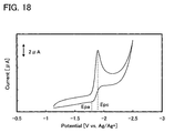
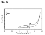
- 238000002484 cyclic voltammetry Methods 0.000 description 8
- 208000015979 hopping Diseases 0.000 description 8
- 239000004973 liquid crystal related substance Substances 0.000 description 8
- PQXKHYXIUOZZFA-UHFFFAOYSA-M lithium fluoride Chemical compound [Li+].[F-] PQXKHYXIUOZZFA-UHFFFAOYSA-M 0.000 description 8
- 229910052814 silicon oxide Inorganic materials 0.000 description 8
- FQJQNLKWTRGIEB-UHFFFAOYSA-N 2-(4-tert-butylphenyl)-5-[3-[5-(4-tert-butylphenyl)-1,3,4-oxadiazol-2-yl]phenyl]-1,3,4-oxadiazole Chemical compound C1=CC(C(C)(C)C)=CC=C1C1=NN=C(C=2C=C(C=CC=2)C=2OC(=NN=2)C=2C=CC(=CC=2)C(C)(C)C)O1 FQJQNLKWTRGIEB-UHFFFAOYSA-N 0.000 description 7
- GEQBRULPNIVQPP-UHFFFAOYSA-N 2-[3,5-bis(1-phenylbenzimidazol-2-yl)phenyl]-1-phenylbenzimidazole Chemical compound C1=CC=CC=C1N1C2=CC=CC=C2N=C1C1=CC(C=2N(C3=CC=CC=C3N=2)C=2C=CC=CC=2)=CC(C=2N(C3=CC=CC=C3N=2)C=2C=CC=CC=2)=C1 GEQBRULPNIVQPP-UHFFFAOYSA-N 0.000 description 7
- GQVWHWAWLPCBHB-UHFFFAOYSA-L beryllium;benzo[h]quinolin-10-olate Chemical compound [Be+2].C1=CC=NC2=C3C([O-])=CC=CC3=CC=C21.C1=CC=NC2=C3C([O-])=CC=CC3=CC=C21 GQVWHWAWLPCBHB-UHFFFAOYSA-L 0.000 description 7
- 150000002484 inorganic compounds Chemical class 0.000 description 7
- 229910010272 inorganic material Inorganic materials 0.000 description 7
- MILUBEOXRNEUHS-UHFFFAOYSA-N iridium(3+) Chemical compound [Ir+3] MILUBEOXRNEUHS-UHFFFAOYSA-N 0.000 description 7
- AJNJGJDDJIBTBP-UHFFFAOYSA-N n-(9,10-diphenylanthracen-2-yl)-n,9-diphenylcarbazol-3-amine Chemical compound C1=CC=CC=C1N(C=1C=C2C(C=3C=CC=CC=3)=C3C=CC=CC3=C(C=3C=CC=CC=3)C2=CC=1)C1=CC=C(N(C=2C=CC=CC=2)C=2C3=CC=CC=2)C3=C1 AJNJGJDDJIBTBP-UHFFFAOYSA-N 0.000 description 7
- QGLKJKCYBOYXKC-UHFFFAOYSA-N nonaoxidotritungsten Chemical compound O=[W]1(=O)O[W](=O)(=O)O[W](=O)(=O)O1 QGLKJKCYBOYXKC-UHFFFAOYSA-N 0.000 description 7
- 239000000047 product Substances 0.000 description 7
- 239000004065 semiconductor Substances 0.000 description 7
- 229910001930 tungsten oxide Inorganic materials 0.000 description 7
- 238000007738 vacuum evaporation Methods 0.000 description 7
- HDMYKJVSQIHZLM-UHFFFAOYSA-N 1-[3,5-di(pyren-1-yl)phenyl]pyrene Chemical compound C1=CC(C=2C=C(C=C(C=2)C=2C3=CC=C4C=CC=C5C=CC(C3=C54)=CC=2)C=2C3=CC=C4C=CC=C5C=CC(C3=C54)=CC=2)=C2C=CC3=CC=CC4=CC=C1C2=C43 HDMYKJVSQIHZLM-UHFFFAOYSA-N 0.000 description 6
- OKKJLVBELUTLKV-UHFFFAOYSA-N Methanol Chemical compound OC OKKJLVBELUTLKV-UHFFFAOYSA-N 0.000 description 6
- SORGEQQSQGNZFI-UHFFFAOYSA-N [azido(phenoxy)phosphoryl]oxybenzene Chemical compound C=1C=CC=CC=1OP(=O)(N=[N+]=[N-])OC1=CC=CC=C1 SORGEQQSQGNZFI-UHFFFAOYSA-N 0.000 description 6
- REDXJYDRNCIFBQ-UHFFFAOYSA-N aluminium(3+) Chemical compound [Al+3] REDXJYDRNCIFBQ-UHFFFAOYSA-N 0.000 description 6
- 230000006399 behavior Effects 0.000 description 6
- 230000015572 biosynthetic process Effects 0.000 description 6
- 230000000052 comparative effect Effects 0.000 description 6
- 230000007423 decrease Effects 0.000 description 6
- ZUOUZKKEUPVFJK-UHFFFAOYSA-N diphenyl Chemical compound C1=CC=CC=C1C1=CC=CC=C1 ZUOUZKKEUPVFJK-UHFFFAOYSA-N 0.000 description 6
- 230000005281 excited state Effects 0.000 description 6
- 238000002347 injection Methods 0.000 description 6
- 239000007924 injection Substances 0.000 description 6
- 238000004519 manufacturing process Methods 0.000 description 6
- 229910052761 rare earth metal Inorganic materials 0.000 description 6
- 239000003566 sealing material Substances 0.000 description 6
- IYZMXHQDXZKNCY-UHFFFAOYSA-N 1-n,1-n-diphenyl-4-n,4-n-bis[4-(n-phenylanilino)phenyl]benzene-1,4-diamine Chemical compound C1=CC=CC=C1N(C=1C=CC(=CC=1)N(C=1C=CC(=CC=1)N(C=1C=CC=CC=1)C=1C=CC=CC=1)C=1C=CC(=CC=1)N(C=1C=CC=CC=1)C=1C=CC=CC=1)C1=CC=CC=C1 IYZMXHQDXZKNCY-UHFFFAOYSA-N 0.000 description 5
- VPYOROSRDYVFDU-UHFFFAOYSA-N 2,3,5,8-tetraphenylquinoxaline Chemical compound C1=CC=CC=C1C(C1=NC(=C(C=2C=CC=CC=2)N=C11)C=2C=CC=CC=2)=CC=C1C1=CC=CC=C1 VPYOROSRDYVFDU-UHFFFAOYSA-N 0.000 description 5
- FYYHWMGAXLPEAU-UHFFFAOYSA-N Magnesium Chemical compound [Mg] FYYHWMGAXLPEAU-UHFFFAOYSA-N 0.000 description 5
- NRTOMJZYCJJWKI-UHFFFAOYSA-N Titanium nitride Chemical compound [Ti]#N NRTOMJZYCJJWKI-UHFFFAOYSA-N 0.000 description 5
- 239000012298 atmosphere Substances 0.000 description 5
- 230000008859 change Effects 0.000 description 5
- 238000002425 crystallisation Methods 0.000 description 5
- 230000008025 crystallization Effects 0.000 description 5
- 239000002019 doping agent Substances 0.000 description 5
- 230000005684 electric field Effects 0.000 description 5
- 210000000540 fraction c Anatomy 0.000 description 5
- 230000006872 improvement Effects 0.000 description 5
- 229910052749 magnesium Inorganic materials 0.000 description 5
- 239000012299 nitrogen atmosphere Substances 0.000 description 5
- 238000007254 oxidation reaction Methods 0.000 description 5
- 238000005192 partition Methods 0.000 description 5
- 230000000737 periodic effect Effects 0.000 description 5
- 125000001997 phenyl group Chemical group [H]C1=C([H])C([H])=C(*)C([H])=C1[H] 0.000 description 5
- 229920003227 poly(N-vinyl carbazole) Polymers 0.000 description 5
- 150000002910 rare earth metals Chemical class 0.000 description 5
- 238000007789 sealing Methods 0.000 description 5
- ODHXBMXNKOYIBV-UHFFFAOYSA-N triphenylamine Chemical compound C1=CC=CC=C1N(C=1C=CC=CC=1)C1=CC=CC=C1 ODHXBMXNKOYIBV-UHFFFAOYSA-N 0.000 description 5
- 239000011787 zinc oxide Substances 0.000 description 5
- IXHWGNYCZPISET-UHFFFAOYSA-N 2-[4-(dicyanomethylidene)-2,3,5,6-tetrafluorocyclohexa-2,5-dien-1-ylidene]propanedinitrile Chemical compound FC1=C(F)C(=C(C#N)C#N)C(F)=C(F)C1=C(C#N)C#N IXHWGNYCZPISET-UHFFFAOYSA-N 0.000 description 4
- OYPRJOBELJOOCE-UHFFFAOYSA-N Calcium Chemical compound [Ca] OYPRJOBELJOOCE-UHFFFAOYSA-N 0.000 description 4
- 229910052693 Europium Inorganic materials 0.000 description 4
- WHXSMMKQMYFTQS-UHFFFAOYSA-N Lithium Chemical compound [Li] WHXSMMKQMYFTQS-UHFFFAOYSA-N 0.000 description 4
- XHCLAFWTIXFWPH-UHFFFAOYSA-N [O-2].[O-2].[O-2].[O-2].[O-2].[V+5].[V+5] Chemical compound [O-2].[O-2].[O-2].[O-2].[O-2].[V+5].[V+5] XHCLAFWTIXFWPH-UHFFFAOYSA-N 0.000 description 4
- 239000004305 biphenyl Substances 0.000 description 4
- UFVXQDWNSAGPHN-UHFFFAOYSA-K bis[(2-methylquinolin-8-yl)oxy]-(4-phenylphenoxy)alumane Chemical compound [Al+3].C1=CC=C([O-])C2=NC(C)=CC=C21.C1=CC=C([O-])C2=NC(C)=CC=C21.C1=CC([O-])=CC=C1C1=CC=CC=C1 UFVXQDWNSAGPHN-UHFFFAOYSA-K 0.000 description 4
- 229910052792 caesium Inorganic materials 0.000 description 4
- TVFDJXOCXUVLDH-UHFFFAOYSA-N caesium atom Chemical compound [Cs] TVFDJXOCXUVLDH-UHFFFAOYSA-N 0.000 description 4
- XJHCXCQVJFPJIK-UHFFFAOYSA-M caesium fluoride Chemical compound [F-].[Cs+] XJHCXCQVJFPJIK-UHFFFAOYSA-M 0.000 description 4
- 229910052791 calcium Inorganic materials 0.000 description 4
- 239000003086 colorant Substances 0.000 description 4
- 239000000412 dendrimer Substances 0.000 description 4
- 229920000736 dendritic polymer Polymers 0.000 description 4
- 238000000151 deposition Methods 0.000 description 4
- 238000011161 development Methods 0.000 description 4
- OGPBJKLSAFTDLK-UHFFFAOYSA-N europium atom Chemical compound [Eu] OGPBJKLSAFTDLK-UHFFFAOYSA-N 0.000 description 4
- 238000004770 highest occupied molecular orbital Methods 0.000 description 4
- 239000001257 hydrogen Substances 0.000 description 4
- 229910052739 hydrogen Inorganic materials 0.000 description 4
- AMWRITDGCCNYAT-UHFFFAOYSA-L hydroxy(oxo)manganese;manganese Chemical compound [Mn].O[Mn]=O.O[Mn]=O AMWRITDGCCNYAT-UHFFFAOYSA-L 0.000 description 4
- 229910003437 indium oxide Inorganic materials 0.000 description 4
- PJXISJQVUVHSOJ-UHFFFAOYSA-N indium(iii) oxide Chemical compound [O-2].[O-2].[O-2].[In+3].[In+3] PJXISJQVUVHSOJ-UHFFFAOYSA-N 0.000 description 4
- 229910052744 lithium Inorganic materials 0.000 description 4
- 150000002739 metals Chemical class 0.000 description 4
- 230000003647 oxidation Effects 0.000 description 4
- 229920003023 plastic Polymers 0.000 description 4
- 239000004033 plastic Substances 0.000 description 4
- 229910052697 platinum Inorganic materials 0.000 description 4
- 229920000642 polymer Polymers 0.000 description 4
- 229910052710 silicon Inorganic materials 0.000 description 4
- 239000010703 silicon Substances 0.000 description 4
- 229910052709 silver Inorganic materials 0.000 description 4
- 239000002356 single layer Substances 0.000 description 4
- 239000002904 solvent Substances 0.000 description 4
- 238000004528 spin coating Methods 0.000 description 4
- 229910001935 vanadium oxide Inorganic materials 0.000 description 4
- SPDPTFAJSFKAMT-UHFFFAOYSA-N 1-n-[4-[4-(n-[4-(3-methyl-n-(3-methylphenyl)anilino)phenyl]anilino)phenyl]phenyl]-4-n,4-n-bis(3-methylphenyl)-1-n-phenylbenzene-1,4-diamine Chemical compound CC1=CC=CC(N(C=2C=CC(=CC=2)N(C=2C=CC=CC=2)C=2C=CC(=CC=2)C=2C=CC(=CC=2)N(C=2C=CC=CC=2)C=2C=CC(=CC=2)N(C=2C=C(C)C=CC=2)C=2C=C(C)C=CC=2)C=2C=C(C)C=CC=2)=C1 SPDPTFAJSFKAMT-UHFFFAOYSA-N 0.000 description 3
- STTGYIUESPWXOW-UHFFFAOYSA-N 2,9-dimethyl-4,7-diphenyl-1,10-phenanthroline Chemical compound C=12C=CC3=C(C=4C=CC=CC=4)C=C(C)N=C3C2=NC(C)=CC=1C1=CC=CC=C1 STTGYIUESPWXOW-UHFFFAOYSA-N 0.000 description 3
- UOCMXZLNHQBBOS-UHFFFAOYSA-N 2-(1,3-benzoxazol-2-yl)phenol zinc Chemical compound [Zn].Oc1ccccc1-c1nc2ccccc2o1.Oc1ccccc1-c1nc2ccccc2o1 UOCMXZLNHQBBOS-UHFFFAOYSA-N 0.000 description 3
- OBAJPWYDYFEBTF-UHFFFAOYSA-N 2-tert-butyl-9,10-dinaphthalen-2-ylanthracene Chemical compound C1=CC=CC2=CC(C3=C4C=CC=CC4=C(C=4C=C5C=CC=CC5=CC=4)C4=CC=C(C=C43)C(C)(C)C)=CC=C21 OBAJPWYDYFEBTF-UHFFFAOYSA-N 0.000 description 3
- ZVFQEOPUXVPSLB-UHFFFAOYSA-N 3-(4-tert-butylphenyl)-4-phenyl-5-(4-phenylphenyl)-1,2,4-triazole Chemical compound C1=CC(C(C)(C)C)=CC=C1C(N1C=2C=CC=CC=2)=NN=C1C1=CC=C(C=2C=CC=CC=2)C=C1 ZVFQEOPUXVPSLB-UHFFFAOYSA-N 0.000 description 3
- USIXUMGAHVBSHQ-UHFFFAOYSA-N 9,10-bis(3,5-diphenylphenyl)anthracene Chemical compound C1=CC=CC=C1C1=CC(C=2C=CC=CC=2)=CC(C=2C3=CC=CC=C3C(C=3C=C(C=C(C=3)C=3C=CC=CC=3)C=3C=CC=CC=3)=C3C=CC=CC3=2)=C1 USIXUMGAHVBSHQ-UHFFFAOYSA-N 0.000 description 3
- VIZUPBYFLORCRA-UHFFFAOYSA-N 9,10-dinaphthalen-2-ylanthracene Chemical compound C12=CC=CC=C2C(C2=CC3=CC=CC=C3C=C2)=C(C=CC=C2)C2=C1C1=CC=C(C=CC=C2)C2=C1 VIZUPBYFLORCRA-UHFFFAOYSA-N 0.000 description 3
- SXGIRTCIFPJUEQ-UHFFFAOYSA-N 9-anthracen-9-ylanthracene Chemical group C1=CC=CC2=CC3=CC=CC=C3C(C=3C4=CC=CC=C4C=C4C=CC=CC4=3)=C21 SXGIRTCIFPJUEQ-UHFFFAOYSA-N 0.000 description 3
- 229910017073 AlLi Inorganic materials 0.000 description 3
- UFHFLCQGNIYNRP-UHFFFAOYSA-N Hydrogen Chemical compound [H][H] UFHFLCQGNIYNRP-UHFFFAOYSA-N 0.000 description 3
- ZMXDDKWLCZADIW-UHFFFAOYSA-N N,N-Dimethylformamide Chemical class CN(C)C=O ZMXDDKWLCZADIW-UHFFFAOYSA-N 0.000 description 3
- PXHVJJICTQNCMI-UHFFFAOYSA-N Nickel Chemical compound [Ni] PXHVJJICTQNCMI-UHFFFAOYSA-N 0.000 description 3
- KDLHZDBZIXYQEI-UHFFFAOYSA-N Palladium Chemical compound [Pd] KDLHZDBZIXYQEI-UHFFFAOYSA-N 0.000 description 3
- YNPNZTXNASCQKK-UHFFFAOYSA-N Phenanthrene Natural products C1=CC=C2C3=CC=CC=C3C=CC2=C1 YNPNZTXNASCQKK-UHFFFAOYSA-N 0.000 description 3
- BQCADISMDOOEFD-UHFFFAOYSA-N Silver Chemical compound [Ag] BQCADISMDOOEFD-UHFFFAOYSA-N 0.000 description 3
- 229910052769 Ytterbium Inorganic materials 0.000 description 3
- DGEZNRSVGBDHLK-UHFFFAOYSA-N [1,10]phenanthroline Chemical compound C1=CN=C2C3=NC=CC=C3C=CC2=C1 DGEZNRSVGBDHLK-UHFFFAOYSA-N 0.000 description 3
- 125000005595 acetylacetonate group Chemical group 0.000 description 3
- 150000004945 aromatic hydrocarbons Chemical class 0.000 description 3
- 235000010290 biphenyl Nutrition 0.000 description 3
- XZCJVWCMJYNSQO-UHFFFAOYSA-N butyl pbd Chemical compound C1=CC(C(C)(C)C)=CC=C1C1=NN=C(C=2C=CC(=CC=2)C=2C=CC=CC=2)O1 XZCJVWCMJYNSQO-UHFFFAOYSA-N 0.000 description 3
- 150000001716 carbazoles Chemical class 0.000 description 3
- 238000006243 chemical reaction Methods 0.000 description 3
- 239000011651 chromium Substances 0.000 description 3
- 230000000295 complement effect Effects 0.000 description 3
- 238000005401 electroluminescence Methods 0.000 description 3
- 238000002474 experimental method Methods 0.000 description 3
- 229910044991 metal oxide Inorganic materials 0.000 description 3
- 150000004706 metal oxides Chemical class 0.000 description 3
- AHLBNYSZXLDEJQ-FWEHEUNISA-N orlistat Chemical compound CCCCCCCCCCC[C@H](OC(=O)[C@H](CC(C)C)NC=O)C[C@@H]1OC(=O)[C@H]1CCCCCC AHLBNYSZXLDEJQ-FWEHEUNISA-N 0.000 description 3
- YYMBJDOZVAITBP-UHFFFAOYSA-N rubrene Chemical compound C1=CC=CC=C1C(C1=C(C=2C=CC=CC=2)C2=CC=CC=C2C(C=2C=CC=CC=2)=C11)=C(C=CC=C2)C2=C1C1=CC=CC=C1 YYMBJDOZVAITBP-UHFFFAOYSA-N 0.000 description 3
- 239000004332 silver Substances 0.000 description 3
- 238000003860 storage Methods 0.000 description 3
- 229910052712 strontium Inorganic materials 0.000 description 3
- CIOAGBVUUVVLOB-UHFFFAOYSA-N strontium atom Chemical compound [Sr] CIOAGBVUUVVLOB-UHFFFAOYSA-N 0.000 description 3
- 230000001629 suppression Effects 0.000 description 3
- KBLZDCFTQSIIOH-UHFFFAOYSA-M tetrabutylazanium;perchlorate Chemical compound [O-]Cl(=O)(=O)=O.CCCC[N+](CCCC)(CCCC)CCCC KBLZDCFTQSIIOH-UHFFFAOYSA-M 0.000 description 3
- 238000001771 vacuum deposition Methods 0.000 description 3
- NAWDYIZEMPQZHO-UHFFFAOYSA-N ytterbium Chemical compound [Yb] NAWDYIZEMPQZHO-UHFFFAOYSA-N 0.000 description 3
- YVTHLONGBIQYBO-UHFFFAOYSA-N zinc indium(3+) oxygen(2-) Chemical compound [O--].[Zn++].[In+3] YVTHLONGBIQYBO-UHFFFAOYSA-N 0.000 description 3
- CJGUQZGGEUNPFQ-UHFFFAOYSA-L zinc;2-(1,3-benzothiazol-2-yl)phenolate Chemical compound [Zn+2].[O-]C1=CC=CC=C1C1=NC2=CC=CC=C2S1.[O-]C1=CC=CC=C1C1=NC2=CC=CC=C2S1 CJGUQZGGEUNPFQ-UHFFFAOYSA-L 0.000 description 3
- HTPBWAPZAJWXKY-UHFFFAOYSA-L zinc;quinolin-8-olate Chemical compound [Zn+2].C1=CN=C2C([O-])=CC=CC2=C1.C1=CN=C2C([O-])=CC=CC2=C1 HTPBWAPZAJWXKY-UHFFFAOYSA-L 0.000 description 3
- UHXOHPVVEHBKKT-UHFFFAOYSA-N 1-(2,2-diphenylethenyl)-4-[4-(2,2-diphenylethenyl)phenyl]benzene Chemical group C=1C=C(C=2C=CC(C=C(C=3C=CC=CC=3)C=3C=CC=CC=3)=CC=2)C=CC=1C=C(C=1C=CC=CC=1)C1=CC=CC=C1 UHXOHPVVEHBKKT-UHFFFAOYSA-N 0.000 description 2
- XOYZGLGJSAZOAG-UHFFFAOYSA-N 1-n,1-n,4-n-triphenyl-4-n-[4-[4-(n-[4-(n-phenylanilino)phenyl]anilino)phenyl]phenyl]benzene-1,4-diamine Chemical group C1=CC=CC=C1N(C=1C=CC(=CC=1)N(C=1C=CC=CC=1)C=1C=CC(=CC=1)C=1C=CC(=CC=1)N(C=1C=CC=CC=1)C=1C=CC(=CC=1)N(C=1C=CC=CC=1)C=1C=CC=CC=1)C1=CC=CC=C1 XOYZGLGJSAZOAG-UHFFFAOYSA-N 0.000 description 2
- IZJOTDOLRQTPHC-UHFFFAOYSA-N 2-(4-carbazol-9-ylphenyl)-5-phenyl-1,3,4-oxadiazole Chemical compound C1=CC=CC=C1C1=NN=C(C=2C=CC(=CC=2)N2C3=CC=CC=C3C3=CC=CC=C32)O1 IZJOTDOLRQTPHC-UHFFFAOYSA-N 0.000 description 2
- GRTDQSRHHHDWSQ-UHFFFAOYSA-N 3,6-diphenyl-9-[4-(10-phenylanthracen-9-yl)phenyl]carbazole Chemical compound C1=CC=CC=C1C1=CC=C(N(C=2C=CC(=CC=2)C=2C3=CC=CC=C3C(C=3C=CC=CC=3)=C3C=CC=CC3=2)C=2C3=CC(=CC=2)C=2C=CC=CC=2)C3=C1 GRTDQSRHHHDWSQ-UHFFFAOYSA-N 0.000 description 2
- GYPAGHMQEIUKAO-UHFFFAOYSA-N 4-butyl-n-[4-[4-(n-(4-butylphenyl)anilino)phenyl]phenyl]-n-phenylaniline Chemical compound C1=CC(CCCC)=CC=C1N(C=1C=CC(=CC=1)C=1C=CC(=CC=1)N(C=1C=CC=CC=1)C=1C=CC(CCCC)=CC=1)C1=CC=CC=C1 GYPAGHMQEIUKAO-UHFFFAOYSA-N 0.000 description 2
- FCNCGHJSNVOIKE-UHFFFAOYSA-N 9,10-diphenylanthracene Chemical compound C1=CC=CC=C1C(C1=CC=CC=C11)=C(C=CC=C2)C2=C1C1=CC=CC=C1 FCNCGHJSNVOIKE-UHFFFAOYSA-N 0.000 description 2
- DTGCMKMICLCAQU-UHFFFAOYSA-N 9-[3-[2-(3-phenanthren-9-ylphenyl)ethenyl]phenyl]phenanthrene Chemical compound C1=CC=C2C(C=3C=CC=C(C=3)C=CC=3C=C(C=CC=3)C=3C4=CC=CC=C4C4=CC=CC=C4C=3)=CC3=CC=CC=C3C2=C1 DTGCMKMICLCAQU-UHFFFAOYSA-N 0.000 description 2
- VFUDMQLBKNMONU-UHFFFAOYSA-N 9-[4-(4-carbazol-9-ylphenyl)phenyl]carbazole Chemical group C12=CC=CC=C2C2=CC=CC=C2N1C1=CC=C(C=2C=CC(=CC=2)N2C3=CC=CC=C3C3=CC=CC=C32)C=C1 VFUDMQLBKNMONU-UHFFFAOYSA-N 0.000 description 2
- HOGUGXVETSOMRE-UHFFFAOYSA-N 9-[4-[2-(4-phenanthren-9-ylphenyl)ethenyl]phenyl]phenanthrene Chemical compound C1=CC=C2C(C3=CC=C(C=C3)C=CC=3C=CC(=CC=3)C=3C4=CC=CC=C4C4=CC=CC=C4C=3)=CC3=CC=CC=C3C2=C1 HOGUGXVETSOMRE-UHFFFAOYSA-N 0.000 description 2
- XKRFYHLGVUSROY-UHFFFAOYSA-N Argon Chemical compound [Ar] XKRFYHLGVUSROY-UHFFFAOYSA-N 0.000 description 2
- IJGRMHOSHXDMSA-UHFFFAOYSA-N Atomic nitrogen Chemical compound N#N IJGRMHOSHXDMSA-UHFFFAOYSA-N 0.000 description 2
- ZKHISQHQYQCSJE-UHFFFAOYSA-N C1=CC=CC=C1N(C=1C=CC(=CC=1)N(C=1C=CC=CC=1)C=1C=C(C=C(C=1)N(C=1C=CC=CC=1)C=1C=CC(=CC=1)N(C=1C=CC=CC=1)C=1C=CC=CC=1)N(C=1C=CC=CC=1)C=1C=CC(=CC=1)N(C=1C=CC=CC=1)C=1C=CC=CC=1)C1=CC=CC=C1 Chemical compound C1=CC=CC=C1N(C=1C=CC(=CC=1)N(C=1C=CC=CC=1)C=1C=C(C=C(C=1)N(C=1C=CC=CC=1)C=1C=CC(=CC=1)N(C=1C=CC=CC=1)C=1C=CC=CC=1)N(C=1C=CC=CC=1)C=1C=CC(=CC=1)N(C=1C=CC=CC=1)C=1C=CC=CC=1)C1=CC=CC=C1 ZKHISQHQYQCSJE-UHFFFAOYSA-N 0.000 description 2
- VYZAMTAEIAYCRO-UHFFFAOYSA-N Chromium Chemical compound [Cr] VYZAMTAEIAYCRO-UHFFFAOYSA-N 0.000 description 2
- VUMVABVDHWICAZ-UHFFFAOYSA-N N-phenyl-N-[4-[4-[N-(9,9'-spirobi[fluorene]-2-yl)anilino]phenyl]phenyl]-9,9'-spirobi[fluorene]-2-amine Chemical compound C1=CC=CC=C1N(C=1C=C2C3(C4=CC=CC=C4C4=CC=CC=C43)C3=CC=CC=C3C2=CC=1)C1=CC=C(C=2C=CC(=CC=2)N(C=2C=CC=CC=2)C=2C=C3C4(C5=CC=CC=C5C5=CC=CC=C54)C4=CC=CC=C4C3=CC=2)C=C1 VUMVABVDHWICAZ-UHFFFAOYSA-N 0.000 description 2
- 229920001609 Poly(3,4-ethylenedioxythiophene) Polymers 0.000 description 2
- XUIMIQQOPSSXEZ-UHFFFAOYSA-N Silicon Chemical compound [Si] XUIMIQQOPSSXEZ-UHFFFAOYSA-N 0.000 description 2
- NIXOWILDQLNWCW-UHFFFAOYSA-N acrylic acid group Chemical group C(C=C)(=O)O NIXOWILDQLNWCW-UHFFFAOYSA-N 0.000 description 2
- MWPLVEDNUUSJAV-UHFFFAOYSA-N anthracene Chemical compound C1=CC=CC2=CC3=CC=CC=C3C=C21 MWPLVEDNUUSJAV-UHFFFAOYSA-N 0.000 description 2
- 150000001491 aromatic compounds Chemical class 0.000 description 2
- 230000008901 benefit Effects 0.000 description 2
- FJDQFPXHSGXQBY-UHFFFAOYSA-L caesium carbonate Chemical compound [Cs+].[Cs+].[O-]C([O-])=O FJDQFPXHSGXQBY-UHFFFAOYSA-L 0.000 description 2
- 229910000024 caesium carbonate Inorganic materials 0.000 description 2
- 238000004364 calculation method Methods 0.000 description 2
- 229910052804 chromium Inorganic materials 0.000 description 2
- 238000004891 communication Methods 0.000 description 2
- 239000004020 conductor Substances 0.000 description 2
- 239000010949 copper Substances 0.000 description 2
- XCJYREBRNVKWGJ-UHFFFAOYSA-N copper(II) phthalocyanine Chemical compound [Cu+2].C12=CC=CC=C2C(N=C2[N-]C(C3=CC=CC=C32)=N2)=NC1=NC([C]1C=CC=CC1=1)=NC=1N=C1[C]3C=CC=CC3=C2[N-]1 XCJYREBRNVKWGJ-UHFFFAOYSA-N 0.000 description 2
- VPUGDVKSAQVFFS-UHFFFAOYSA-N coronene Chemical compound C1=C(C2=C34)C=CC3=CC=C(C=C3)C4=C4C3=CC=C(C=C3)C4=C2C3=C1 VPUGDVKSAQVFFS-UHFFFAOYSA-N 0.000 description 2
- 239000007772 electrode material Substances 0.000 description 2
- KTWOOEGAPBSYNW-UHFFFAOYSA-N ferrocene Chemical compound [Fe+2].C=1C=C[CH-]C=1.C=1C=C[CH-]C=1 KTWOOEGAPBSYNW-UHFFFAOYSA-N 0.000 description 2
- 239000011152 fibreglass Substances 0.000 description 2
- 239000000945 filler Substances 0.000 description 2
- 239000010931 gold Substances 0.000 description 2
- 150000002391 heterocyclic compounds Chemical class 0.000 description 2
- FUJCRWPEOMXPAD-UHFFFAOYSA-N lithium oxide Chemical compound [Li+].[Li+].[O-2] FUJCRWPEOMXPAD-UHFFFAOYSA-N 0.000 description 2
- 229910001947 lithium oxide Inorganic materials 0.000 description 2
- 238000004020 luminiscence type Methods 0.000 description 2
- 239000007769 metal material Substances 0.000 description 2
- FQPSGWSUVKBHSU-UHFFFAOYSA-N methacrylamide Chemical compound CC(=C)C(N)=O FQPSGWSUVKBHSU-UHFFFAOYSA-N 0.000 description 2
- VZYZZKOUCVXTOJ-UHFFFAOYSA-N n-[4-[4-(n-(9,9-dimethylfluoren-2-yl)anilino)phenyl]phenyl]-9,9-dimethyl-n-phenylfluoren-2-amine Chemical group C1=C2C(C)(C)C3=CC=CC=C3C2=CC=C1N(C=1C=CC(=CC=1)C=1C=CC(=CC=1)N(C=1C=CC=CC=1)C=1C=C2C(C)(C)C3=CC=CC=C3C2=CC=1)C1=CC=CC=C1 VZYZZKOUCVXTOJ-UHFFFAOYSA-N 0.000 description 2
- 230000033116 oxidation-reduction process Effects 0.000 description 2
- DYIZHKNUQPHNJY-UHFFFAOYSA-N oxorhenium Chemical compound [Re]=O DYIZHKNUQPHNJY-UHFFFAOYSA-N 0.000 description 2
- YRZZLAGRKZIJJI-UHFFFAOYSA-N oxyvanadium phthalocyanine Chemical compound [V+2]=O.C12=CC=CC=C2C(N=C2[N-]C(C3=CC=CC=C32)=N2)=NC1=NC([C]1C=CC=CC1=1)=NC=1N=C1[C]3C=CC=CC3=C2[N-]1 YRZZLAGRKZIJJI-UHFFFAOYSA-N 0.000 description 2
- IEQIEDJGQAUEQZ-UHFFFAOYSA-N phthalocyanine Chemical compound N1C(N=C2C3=CC=CC=C3C(N=C3C4=CC=CC=C4C(=N4)N3)=N2)=C(C=CC=C2)C2=C1N=C1C2=CC=CC=C2C4=N1 IEQIEDJGQAUEQZ-UHFFFAOYSA-N 0.000 description 2
- SIOXPEMLGUPBBT-UHFFFAOYSA-M picolinate Chemical compound [O-]C(=O)C1=CC=CC=N1 SIOXPEMLGUPBBT-UHFFFAOYSA-M 0.000 description 2
- 229920000078 poly(4-vinyltriphenylamine) Polymers 0.000 description 2
- 229920000553 poly(phenylenevinylene) Polymers 0.000 description 2
- 229920000172 poly(styrenesulfonic acid) Polymers 0.000 description 2
- 229920002620 polyvinyl fluoride Polymers 0.000 description 2
- 230000008569 process Effects 0.000 description 2
- 238000010791 quenching Methods 0.000 description 2
- 230000000171 quenching effect Effects 0.000 description 2
- 229910003449 rhenium oxide Inorganic materials 0.000 description 2
- 229910001925 ruthenium oxide Inorganic materials 0.000 description 2
- WOCIAKWEIIZHES-UHFFFAOYSA-N ruthenium(iv) oxide Chemical compound O=[Ru]=O WOCIAKWEIIZHES-UHFFFAOYSA-N 0.000 description 2
- 238000003980 solgel method Methods 0.000 description 2
- 239000010936 titanium Substances 0.000 description 2
- WFKWXMTUELFFGS-UHFFFAOYSA-N tungsten Chemical compound [W] WFKWXMTUELFFGS-UHFFFAOYSA-N 0.000 description 2
- 229910052721 tungsten Inorganic materials 0.000 description 2
- 239000010937 tungsten Substances 0.000 description 2
- IWZZBBJTIUYDPZ-DVACKJPTSA-N (z)-4-hydroxypent-3-en-2-one;iridium;2-phenylpyridine Chemical compound [Ir].C\C(O)=C\C(C)=O.[C-]1=CC=CC=C1C1=CC=CC=N1.[C-]1=CC=CC=C1C1=CC=CC=N1 IWZZBBJTIUYDPZ-DVACKJPTSA-N 0.000 description 1
- POILWHVDKZOXJZ-ARJAWSKDSA-M (z)-4-oxopent-2-en-2-olate Chemical compound C\C([O-])=C\C(C)=O POILWHVDKZOXJZ-ARJAWSKDSA-M 0.000 description 1
- RTSZQXSYCGBHMO-UHFFFAOYSA-N 1,2,4-trichloro-3-prop-1-ynoxybenzene Chemical compound CC#COC1=C(Cl)C=CC(Cl)=C1Cl RTSZQXSYCGBHMO-UHFFFAOYSA-N 0.000 description 1
- OBMPIWRNYHXYBC-UHFFFAOYSA-N 1-n,1-n,3-n,3-n,5-n,5-n-hexakis(3-methylphenyl)benzene-1,3,5-triamine Chemical compound CC1=CC=CC(N(C=2C=C(C)C=CC=2)C=2C=C(C=C(C=2)N(C=2C=C(C)C=CC=2)C=2C=C(C)C=CC=2)N(C=2C=C(C)C=CC=2)C=2C=C(C)C=CC=2)=C1 OBMPIWRNYHXYBC-UHFFFAOYSA-N 0.000 description 1
- FQNVFRPAQRVHKO-UHFFFAOYSA-N 1-n,4-n-bis(4-methylphenyl)-1-n,4-n-diphenylbenzene-1,4-diamine Chemical compound C1=CC(C)=CC=C1N(C=1C=CC(=CC=1)N(C=1C=CC=CC=1)C=1C=CC(C)=CC=1)C1=CC=CC=C1 FQNVFRPAQRVHKO-UHFFFAOYSA-N 0.000 description 1
- UVAMFBJPMUMURT-UHFFFAOYSA-N 2,3,4,5,6-pentafluorobenzenethiol Chemical compound FC1=C(F)C(F)=C(S)C(F)=C1F UVAMFBJPMUMURT-UHFFFAOYSA-N 0.000 description 1
- OOWLPGTVRWFLCX-UHFFFAOYSA-N 2,3,6,7-tetramethyl-9,10-dinaphthalen-1-ylanthracene Chemical compound C1=CC=C2C(C=3C4=CC(C)=C(C)C=C4C(C=4C5=CC=CC=C5C=CC=4)=C4C=C(C(=CC4=3)C)C)=CC=CC2=C1 OOWLPGTVRWFLCX-UHFFFAOYSA-N 0.000 description 1
- JEBPFDQAOYARIB-UHFFFAOYSA-N 2,3,6,7-tetramethyl-9,10-dinaphthalen-2-ylanthracene Chemical compound C1=CC=CC2=CC(C=3C4=CC(C)=C(C)C=C4C(C=4C=C5C=CC=CC5=CC=4)=C4C=C(C(=CC4=3)C)C)=CC=C21 JEBPFDQAOYARIB-UHFFFAOYSA-N 0.000 description 1
- VMAUSAPAESMXAB-UHFFFAOYSA-N 2,3-bis(4-fluorophenyl)quinoxaline Chemical compound C1=CC(F)=CC=C1C1=NC2=CC=CC=C2N=C1C1=CC=C(F)C=C1 VMAUSAPAESMXAB-UHFFFAOYSA-N 0.000 description 1
- GCVFCMJENJPSIU-UHFFFAOYSA-N 2,3-bis[4-(trifluoromethyl)phenyl]quinoxaline Chemical compound C1=CC(C(F)(F)F)=CC=C1C1=NC2=CC=CC=C2N=C1C1=CC=C(C(F)(F)F)C=C1 GCVFCMJENJPSIU-UHFFFAOYSA-N 0.000 description 1
- RSNQVABHABAKEZ-UHFFFAOYSA-N 2,3-diphenylquinoxaline Chemical compound C1=CC=CC=C1C1=NC2=CC=CC=C2N=C1C1=CC=CC=C1 RSNQVABHABAKEZ-UHFFFAOYSA-N 0.000 description 1
- BFTIPCRZWILUIY-UHFFFAOYSA-N 2,5,8,11-tetratert-butylperylene Chemical group CC(C)(C)C1=CC(C2=CC(C(C)(C)C)=CC=3C2=C2C=C(C=3)C(C)(C)C)=C3C2=CC(C(C)(C)C)=CC3=C1 BFTIPCRZWILUIY-UHFFFAOYSA-N 0.000 description 1
- YLYPIBBGWLKELC-RMKNXTFCSA-N 2-[2-[(e)-2-[4-(dimethylamino)phenyl]ethenyl]-6-methylpyran-4-ylidene]propanedinitrile Chemical compound C1=CC(N(C)C)=CC=C1\C=C\C1=CC(=C(C#N)C#N)C=C(C)O1 YLYPIBBGWLKELC-RMKNXTFCSA-N 0.000 description 1
- ZNJRONVKWRHYBF-UHFFFAOYSA-N 2-[2-[2-(1-azatricyclo[7.3.1.05,13]trideca-5,7,9(13)-trien-7-yl)ethenyl]-6-methylpyran-4-ylidene]propanedinitrile Chemical compound O1C(C)=CC(=C(C#N)C#N)C=C1C=CC1=CC(CCCN2CCC3)=C2C3=C1 ZNJRONVKWRHYBF-UHFFFAOYSA-N 0.000 description 1
- VQGHOUODWALEFC-UHFFFAOYSA-N 2-phenylpyridine Chemical compound C1=CC=CC=C1C1=CC=CC=N1 VQGHOUODWALEFC-UHFFFAOYSA-N 0.000 description 1
- IBHNCJLKIQIKFU-UHFFFAOYSA-N 2-tert-butyl-9,10-bis(2-naphthalen-1-ylphenyl)anthracene Chemical compound C1=CC=C2C(C3=CC=CC=C3C3=C4C=CC=CC4=C(C=4C(=CC=CC=4)C=4C5=CC=CC=C5C=CC=4)C4=CC=C(C=C43)C(C)(C)C)=CC=CC2=C1 IBHNCJLKIQIKFU-UHFFFAOYSA-N 0.000 description 1
- MNHPNCZSKTUPMB-UHFFFAOYSA-N 2-tert-butyl-9,10-bis(4-phenylphenyl)anthracene Chemical compound C=12C=CC=CC2=C(C=2C=CC(=CC=2)C=2C=CC=CC=2)C2=CC(C(C)(C)C)=CC=C2C=1C(C=C1)=CC=C1C1=CC=CC=C1 MNHPNCZSKTUPMB-UHFFFAOYSA-N 0.000 description 1
- ONMVVYFKZFORGI-UHFFFAOYSA-N 2-tert-butyl-9,10-dinaphthalen-1-ylanthracene Chemical compound C1=CC=C2C(C3=C4C=CC=CC4=C(C=4C5=CC=CC=C5C=CC=4)C4=CC=C(C=C43)C(C)(C)C)=CC=CC2=C1 ONMVVYFKZFORGI-UHFFFAOYSA-N 0.000 description 1
- WBPXZSIKOVBSAS-UHFFFAOYSA-N 2-tert-butylanthracene Chemical compound C1=CC=CC2=CC3=CC(C(C)(C)C)=CC=C3C=C21 WBPXZSIKOVBSAS-UHFFFAOYSA-N 0.000 description 1
- TVMBOHMLKCZFFW-UHFFFAOYSA-N 3-N,6-N,9-triphenyl-3-N,6-N-bis(9-phenylcarbazol-3-yl)carbazole-3,6-diamine Chemical compound C1=CC=CC=C1N(C=1C=C2C3=CC(=CC=C3N(C=3C=CC=CC=3)C2=CC=1)N(C=1C=CC=CC=1)C=1C=C2C3=CC=CC=C3N(C=3C=CC=CC=3)C2=CC=1)C1=CC=C(N(C=2C=CC=CC=2)C=2C3=CC=CC=2)C3=C1 TVMBOHMLKCZFFW-UHFFFAOYSA-N 0.000 description 1
- OGGKVJMNFFSDEV-UHFFFAOYSA-N 3-methyl-n-[4-[4-(n-(3-methylphenyl)anilino)phenyl]phenyl]-n-phenylaniline Chemical compound CC1=CC=CC(N(C=2C=CC=CC=2)C=2C=CC(=CC=2)C=2C=CC(=CC=2)N(C=2C=CC=CC=2)C=2C=C(C)C=CC=2)=C1 OGGKVJMNFFSDEV-UHFFFAOYSA-N 0.000 description 1
- RJTHHXBWBYVRSI-UHFFFAOYSA-N 4,19-dimethyl-4,19-diazaheptacyclo[16.12.0.03,16.05,14.06,11.020,29.021,26]triaconta-1,3(16),5(14),6,8,10,12,17,20(29),21,23,25,27-tridecaene-15,30-dione Chemical compound C1=CC=CC2=CC=C(C(C=3C=C4N(C5=C6C=CC=CC6=CC=C5C(=O)C4=CC=3N3C)C)=O)C3=C21 RJTHHXBWBYVRSI-UHFFFAOYSA-N 0.000 description 1
- HXWWMGJBPGRWRS-CMDGGOBGSA-N 4- -2-tert-butyl-6- -4h-pyran Chemical compound O1C(C(C)(C)C)=CC(=C(C#N)C#N)C=C1\C=C\C1=CC(C(CCN2CCC3(C)C)(C)C)=C2C3=C1 HXWWMGJBPGRWRS-CMDGGOBGSA-N 0.000 description 1
- YLYPIBBGWLKELC-UHFFFAOYSA-N 4-(dicyanomethylene)-2-methyl-6-(4-(dimethylamino)styryl)-4H-pyran Chemical compound C1=CC(N(C)C)=CC=C1C=CC1=CC(=C(C#N)C#N)C=C(C)O1 YLYPIBBGWLKELC-UHFFFAOYSA-N 0.000 description 1
- ZNJRONVKWRHYBF-VOTSOKGWSA-N 4-(dicyanomethylene)-2-methyl-6-julolidyl-9-enyl-4h-pyran Chemical compound O1C(C)=CC(=C(C#N)C#N)C=C1\C=C\C1=CC(CCCN2CCC3)=C2C3=C1 ZNJRONVKWRHYBF-VOTSOKGWSA-N 0.000 description 1
- AWXGSYPUMWKTBR-UHFFFAOYSA-N 4-carbazol-9-yl-n,n-bis(4-carbazol-9-ylphenyl)aniline Chemical compound C12=CC=CC=C2C2=CC=CC=C2N1C1=CC=C(N(C=2C=CC(=CC=2)N2C3=CC=CC=C3C3=CC=CC=C32)C=2C=CC(=CC=2)N2C3=CC=CC=C3C3=CC=CC=C32)C=C1 AWXGSYPUMWKTBR-UHFFFAOYSA-N 0.000 description 1
- HGHBHXZNXIDZIZ-UHFFFAOYSA-N 4-n-(9,10-diphenylanthracen-2-yl)-1-n,1-n,4-n-triphenylbenzene-1,4-diamine Chemical compound C1=CC=CC=C1N(C=1C=CC(=CC=1)N(C=1C=CC=CC=1)C=1C=C2C(C=3C=CC=CC=3)=C3C=CC=CC3=C(C=3C=CC=CC=3)C2=CC=1)C1=CC=CC=C1 HGHBHXZNXIDZIZ-UHFFFAOYSA-N 0.000 description 1
- KLNDKWAYVMOOFU-UHFFFAOYSA-N 4-n-[9,10-bis(2-phenylphenyl)anthracen-2-yl]-1-n,1-n,4-n-triphenylbenzene-1,4-diamine Chemical compound C1=CC=CC=C1N(C=1C=CC(=CC=1)N(C=1C=CC=CC=1)C=1C=C2C(C=3C(=CC=CC=3)C=3C=CC=CC=3)=C3C=CC=CC3=C(C=3C(=CC=CC=3)C=3C=CC=CC=3)C2=CC=1)C1=CC=CC=C1 KLNDKWAYVMOOFU-UHFFFAOYSA-N 0.000 description 1
- SCZWJXTUYYSKGF-UHFFFAOYSA-N 5,12-dimethylquinolino[2,3-b]acridine-7,14-dione Chemical compound CN1C2=CC=CC=C2C(=O)C2=C1C=C1C(=O)C3=CC=CC=C3N(C)C1=C2 SCZWJXTUYYSKGF-UHFFFAOYSA-N 0.000 description 1
- KIYZNTXHGDXHQH-UHFFFAOYSA-N 5,12-diphenyl-6,11-bis(4-phenylphenyl)tetracene Chemical compound C1=CC=CC=C1C1=CC=C(C=2C3=C(C=4C=CC=CC=4)C4=CC=CC=C4C(C=4C=CC=CC=4)=C3C(C=3C=CC(=CC=3)C=3C=CC=CC=3)=C3C=CC=CC3=2)C=C1 KIYZNTXHGDXHQH-UHFFFAOYSA-N 0.000 description 1
- HKHMXTFNINVDFI-UHFFFAOYSA-N 5,12-diphenylquinolino[2,3-b]acridine-7,14-dione Chemical compound C12=CC(C(C3=CC=CC=C3N3C=4C=CC=CC=4)=O)=C3C=C2C(=O)C2=CC=CC=C2N1C1=CC=CC=C1 HKHMXTFNINVDFI-UHFFFAOYSA-N 0.000 description 1
- TYGSHIPXFUQBJO-UHFFFAOYSA-N 5-n,5-n,11-n,11-n-tetrakis(4-methylphenyl)tetracene-5,11-diamine Chemical compound C1=CC(C)=CC=C1N(C=1C2=CC3=CC=CC=C3C(N(C=3C=CC(C)=CC=3)C=3C=CC(C)=CC=3)=C2C=C2C=CC=CC2=1)C1=CC=C(C)C=C1 TYGSHIPXFUQBJO-UHFFFAOYSA-N 0.000 description 1
- MWQDBYKWEGXSJW-UHFFFAOYSA-N 6,12-dimethoxy-5,11-diphenylchrysene Chemical compound C12=C3C=CC=CC3=C(OC)C(C=3C=CC=CC=3)=C2C2=CC=CC=C2C(OC)=C1C1=CC=CC=C1 MWQDBYKWEGXSJW-UHFFFAOYSA-N 0.000 description 1
- QESBRXIXJOBVGC-UHFFFAOYSA-N 6-(2,3-diphenylquinoxalin-6-yl)-2,3-diphenylquinoxaline Chemical compound C1=CC=CC=C1C1=NC2=CC=C(C=3C=C4N=C(C(C=5C=CC=CC=5)=NC4=CC=3)C=3C=CC=CC=3)C=C2N=C1C1=CC=CC=C1 QESBRXIXJOBVGC-UHFFFAOYSA-N 0.000 description 1
- APDXFZFRIJSGRC-UHFFFAOYSA-N 6-[2,3-bis(4-fluorophenyl)quinoxalin-6-yl]-2,3-bis(4-fluorophenyl)quinoxaline Chemical compound C1=CC(F)=CC=C1C1=NC2=CC=C(C=3C=C4N=C(C(C=5C=CC(F)=CC=5)=NC4=CC=3)C=3C=CC(F)=CC=3)C=C2N=C1C1=CC=C(F)C=C1 APDXFZFRIJSGRC-UHFFFAOYSA-N 0.000 description 1
- NKEZXXDRXPPROK-UHFFFAOYSA-N 9,10-bis(2-naphthalen-1-ylphenyl)anthracene Chemical compound C12=CC=CC=C2C(C2=CC=CC=C2C=2C3=CC=CC=C3C=CC=2)=C(C=CC=C2)C2=C1C1=CC=CC=C1C1=CC=CC2=CC=CC=C12 NKEZXXDRXPPROK-UHFFFAOYSA-N 0.000 description 1
- YTSGZCWSEMDTBC-UHFFFAOYSA-N 9,10-bis(4-methylnaphthalen-1-yl)anthracene Chemical compound C12=CC=CC=C2C(C)=CC=C1C(C1=CC=CC=C11)=C(C=CC=C2)C2=C1C1=CC=C(C)C2=CC=CC=C12 YTSGZCWSEMDTBC-UHFFFAOYSA-N 0.000 description 1
- BITWULPDIGXQDL-UHFFFAOYSA-N 9,10-bis[4-(2,2-diphenylethenyl)phenyl]anthracene Chemical compound C=1C=C(C=2C3=CC=CC=C3C(C=3C=CC(C=C(C=4C=CC=CC=4)C=4C=CC=CC=4)=CC=3)=C3C=CC=CC3=2)C=CC=1C=C(C=1C=CC=CC=1)C1=CC=CC=C1 BITWULPDIGXQDL-UHFFFAOYSA-N 0.000 description 1
- OEYLQYLOSLLBTR-UHFFFAOYSA-N 9-(2-phenylphenyl)-10-[10-(2-phenylphenyl)anthracen-9-yl]anthracene Chemical group C1=CC=CC=C1C1=CC=CC=C1C(C1=CC=CC=C11)=C(C=CC=C2)C2=C1C(C1=CC=CC=C11)=C(C=CC=C2)C2=C1C1=CC=CC=C1C1=CC=CC=C1 OEYLQYLOSLLBTR-UHFFFAOYSA-N 0.000 description 1
- XCICDYGIJBPNPC-UHFFFAOYSA-N 9-[4-[3,5-bis(4-carbazol-9-ylphenyl)phenyl]phenyl]carbazole Chemical compound C12=CC=CC=C2C2=CC=CC=C2N1C1=CC=C(C=2C=C(C=C(C=2)C=2C=CC(=CC=2)N2C3=CC=CC=C3C3=CC=CC=C32)C=2C=CC(=CC=2)N2C3=CC=CC=C3C3=CC=CC=C32)C=C1 XCICDYGIJBPNPC-UHFFFAOYSA-N 0.000 description 1
- ZWSVEGKGLOHGIQ-UHFFFAOYSA-N 9-[4-[4-(4-carbazol-9-ylphenyl)-2,3,5,6-tetraphenylphenyl]phenyl]carbazole Chemical compound C1=CC=CC=C1C(C(=C(C=1C=CC=CC=1)C(C=1C=CC=CC=1)=C1C=2C=CC(=CC=2)N2C3=CC=CC=C3C3=CC=CC=C32)C=2C=CC(=CC=2)N2C3=CC=CC=C3C3=CC=CC=C32)=C1C1=CC=CC=C1 ZWSVEGKGLOHGIQ-UHFFFAOYSA-N 0.000 description 1
- NBYGJKGEGNTQBK-UHFFFAOYSA-N 9-phenyl-10-(10-phenylanthracen-9-yl)anthracene Chemical group C1=CC=CC=C1C(C1=CC=CC=C11)=C(C=CC=C2)C2=C1C(C1=CC=CC=C11)=C(C=CC=C2)C2=C1C1=CC=CC=C1 NBYGJKGEGNTQBK-UHFFFAOYSA-N 0.000 description 1
- AEEPLSWKIVXXLE-UHFFFAOYSA-N 9-phenyl-3-[9-[4-(10-phenylanthracen-9-yl)phenyl]carbazol-3-yl]carbazole Chemical compound C1=CC=CC=C1C(C1=CC=CC=C11)=C(C=CC=C2)C2=C1C1=CC=C(N2C3=CC=C(C=C3C3=CC=CC=C32)C=2C=C3C4=CC=CC=C4N(C=4C=CC=CC=4)C3=CC=2)C=C1 AEEPLSWKIVXXLE-UHFFFAOYSA-N 0.000 description 1
- GDALETGZDYOOGB-UHFFFAOYSA-N Acridone Natural products C1=C(O)C=C2N(C)C3=CC=CC=C3C(=O)C2=C1O GDALETGZDYOOGB-UHFFFAOYSA-N 0.000 description 1
- 239000004925 Acrylic resin Substances 0.000 description 1
- 229920000178 Acrylic resin Polymers 0.000 description 1
- 229910000838 Al alloy Inorganic materials 0.000 description 1
- 102100025982 BMP/retinoic acid-inducible neural-specific protein 1 Human genes 0.000 description 1
- BVKZGUZCCUSVTD-UHFFFAOYSA-L Carbonate Chemical compound [O-]C([O-])=O BVKZGUZCCUSVTD-UHFFFAOYSA-L 0.000 description 1
- RYGMFSIKBFXOCR-UHFFFAOYSA-N Copper Chemical compound [Cu] RYGMFSIKBFXOCR-UHFFFAOYSA-N 0.000 description 1
- 239000004593 Epoxy Substances 0.000 description 1
- 101000933342 Homo sapiens BMP/retinoic acid-inducible neural-specific protein 1 Proteins 0.000 description 1
- 101000715194 Homo sapiens Cell cycle and apoptosis regulator protein 2 Proteins 0.000 description 1
- 101000837344 Homo sapiens T-cell leukemia translocation-altered gene protein Proteins 0.000 description 1
- XEEYBQQBJWHFJM-UHFFFAOYSA-N Iron Chemical compound [Fe] XEEYBQQBJWHFJM-UHFFFAOYSA-N 0.000 description 1
- ZOKXTWBITQBERF-UHFFFAOYSA-N Molybdenum Chemical compound [Mo] ZOKXTWBITQBERF-UHFFFAOYSA-N 0.000 description 1
- 102100028692 T-cell leukemia translocation-altered gene protein Human genes 0.000 description 1
- 229910052771 Terbium Inorganic materials 0.000 description 1
- XBDYBAVJXHJMNQ-UHFFFAOYSA-N Tetrahydroanthracene Natural products C1=CC=C2C=C(CCCC3)C3=CC2=C1 XBDYBAVJXHJMNQ-UHFFFAOYSA-N 0.000 description 1
- RTAQQCXQSZGOHL-UHFFFAOYSA-N Titanium Chemical compound [Ti] RTAQQCXQSZGOHL-UHFFFAOYSA-N 0.000 description 1
- WGLPBDUCMAPZCE-UHFFFAOYSA-N Trioxochromium Chemical compound O=[Cr](=O)=O WGLPBDUCMAPZCE-UHFFFAOYSA-N 0.000 description 1
- GBKYFASVJPZWLI-UHFFFAOYSA-N [Pt+2].N1C(C=C2C(=C(CC)C(C=C3C(=C(CC)C(=C4)N3)CC)=N2)CC)=C(CC)C(CC)=C1C=C1C(CC)=C(CC)C4=N1 Chemical compound [Pt+2].N1C(C=C2C(=C(CC)C(C=C3C(=C(CC)C(=C4)N3)CC)=N2)CC)=C(CC)C(CC)=C1C=C1C(CC)=C(CC)C4=N1 GBKYFASVJPZWLI-UHFFFAOYSA-N 0.000 description 1
- 239000002253 acid Substances 0.000 description 1
- FZEYVTFCMJSGMP-UHFFFAOYSA-N acridone Chemical compound C1=CC=C2C(=O)C3=CC=CC=C3NC2=C1 FZEYVTFCMJSGMP-UHFFFAOYSA-N 0.000 description 1
- 230000002411 adverse Effects 0.000 description 1
- 230000002776 aggregation Effects 0.000 description 1
- 238000004220 aggregation Methods 0.000 description 1
- 229920000109 alkoxy-substituted poly(p-phenylene vinylene) Polymers 0.000 description 1
- 150000001454 anthracenes Chemical class 0.000 description 1
- 229910052786 argon Inorganic materials 0.000 description 1
- QVGXLLKOCUKJST-UHFFFAOYSA-N atomic oxygen Chemical compound [O] QVGXLLKOCUKJST-UHFFFAOYSA-N 0.000 description 1
- HXWWMGJBPGRWRS-UHFFFAOYSA-N b2738 Chemical compound O1C(C(C)(C)C)=CC(=C(C#N)C#N)C=C1C=CC1=CC(C(CCN2CCC3(C)C)(C)C)=C2C3=C1 HXWWMGJBPGRWRS-UHFFFAOYSA-N 0.000 description 1
- 125000005605 benzo group Chemical group 0.000 description 1
- 230000000903 blocking effect Effects 0.000 description 1
- WUKWITHWXAAZEY-UHFFFAOYSA-L calcium difluoride Chemical compound [F-].[F-].[Ca+2] WUKWITHWXAAZEY-UHFFFAOYSA-L 0.000 description 1
- 239000010406 cathode material Substances 0.000 description 1
- 229910000423 chromium oxide Inorganic materials 0.000 description 1
- 229910017052 cobalt Inorganic materials 0.000 description 1
- 239000010941 cobalt Substances 0.000 description 1
- GUTLYIVDDKVIGB-UHFFFAOYSA-N cobalt atom Chemical compound [Co] GUTLYIVDDKVIGB-UHFFFAOYSA-N 0.000 description 1
- 238000007796 conventional method Methods 0.000 description 1
- 229910052802 copper Inorganic materials 0.000 description 1
- VSSSHNJONFTXHS-UHFFFAOYSA-N coumarin 153 Chemical compound C12=C3CCCN2CCCC1=CC1=C3OC(=O)C=C1C(F)(F)F VSSSHNJONFTXHS-UHFFFAOYSA-N 0.000 description 1
- JRUYYVYCSJCVMP-UHFFFAOYSA-N coumarin 30 Chemical compound C1=CC=C2N(C)C(C=3C4=CC=C(C=C4OC(=O)C=3)N(CC)CC)=NC2=C1 JRUYYVYCSJCVMP-UHFFFAOYSA-N 0.000 description 1
- XHXMPURWMSJENN-UHFFFAOYSA-N coumarin 480 Chemical compound C12=C3CCCN2CCCC1=CC1=C3OC(=O)C=C1C XHXMPURWMSJENN-UHFFFAOYSA-N 0.000 description 1
- WWZVTLIQPPVZEL-UHFFFAOYSA-N coumarin 480 d Chemical compound C12=C3CCCN2CCCC1=CC1=C3OC(=O)C=C1C(C)C WWZVTLIQPPVZEL-UHFFFAOYSA-N 0.000 description 1
- VBVAVBCYMYWNOU-UHFFFAOYSA-N coumarin 6 Chemical compound C1=CC=C2SC(C3=CC4=CC=C(C=C4OC3=O)N(CC)CC)=NC2=C1 VBVAVBCYMYWNOU-UHFFFAOYSA-N 0.000 description 1
- MZSOXGPKUOAXNY-UHFFFAOYSA-N coumarin 6h Chemical compound C1CCC2=C(OC(=O)C=C3)C3=CC3=C2N1CCC3 MZSOXGPKUOAXNY-UHFFFAOYSA-N 0.000 description 1
- BHQBDOOJEZXHPS-UHFFFAOYSA-N ctk3i0272 Chemical group C1=CC=CC=C1C(C(=C(C=1C=CC=CC=1)C(=C1C=2C=CC=CC=2)C=2C3=CC=CC=C3C(C=3C4=CC=CC=C4C(C=4C(=C(C=5C=CC=CC=5)C(C=5C=CC=CC=5)=C(C=5C=CC=CC=5)C=4C=4C=CC=CC=4)C=4C=CC=CC=4)=C4C=CC=CC4=3)=C3C=CC=CC3=2)C=2C=CC=CC=2)=C1C1=CC=CC=C1 BHQBDOOJEZXHPS-UHFFFAOYSA-N 0.000 description 1
- BRRYGOLATSLUES-UHFFFAOYSA-N ctk5e1271 Chemical compound C1=C2NC3=C4C=CC=CC4=CC=C3C(=O)C2=CC2=C1C(=O)C1=CC=C3C=CC=CC3=C1N2 BRRYGOLATSLUES-UHFFFAOYSA-N 0.000 description 1
- 230000003247 decreasing effect Effects 0.000 description 1
- 238000010586 diagram Methods 0.000 description 1
- 238000009792 diffusion process Methods 0.000 description 1
- 238000009826 distribution Methods 0.000 description 1
- 230000007613 environmental effect Effects 0.000 description 1
- 238000011156 evaluation Methods 0.000 description 1
- 238000000605 extraction Methods 0.000 description 1
- 238000013213 extrapolation Methods 0.000 description 1
- 230000002349 favourable effect Effects 0.000 description 1
- 239000000706 filtrate Substances 0.000 description 1
- 125000005567 fluorenylene group Chemical group 0.000 description 1
- 239000007850 fluorescent dye Substances 0.000 description 1
- PCHJSUWPFVWCPO-UHFFFAOYSA-N gold Chemical compound [Au] PCHJSUWPFVWCPO-UHFFFAOYSA-N 0.000 description 1
- 229910052737 gold Inorganic materials 0.000 description 1
- 230000005283 ground state Effects 0.000 description 1
- 229910052738 indium Inorganic materials 0.000 description 1
- APFVFJFRJDLVQX-UHFFFAOYSA-N indium atom Chemical compound [In] APFVFJFRJDLVQX-UHFFFAOYSA-N 0.000 description 1
- 239000011261 inert gas Substances 0.000 description 1
- CUONGYYJJVDODC-UHFFFAOYSA-N malononitrile Chemical compound N#CCC#N CUONGYYJJVDODC-UHFFFAOYSA-N 0.000 description 1
- 230000007246 mechanism Effects 0.000 description 1
- 229910052750 molybdenum Inorganic materials 0.000 description 1
- 239000011733 molybdenum Substances 0.000 description 1
- WOYDRSOIBHFMGB-UHFFFAOYSA-N n,9-diphenyl-n-(9-phenylcarbazol-3-yl)carbazol-3-amine Chemical compound C1=CC=CC=C1N(C=1C=C2C3=CC=CC=C3N(C=3C=CC=CC=3)C2=CC=1)C1=CC=C(N(C=2C=CC=CC=2)C=2C3=CC=CC=2)C3=C1 WOYDRSOIBHFMGB-UHFFFAOYSA-N 0.000 description 1
- BBNZOXKLBAWRSH-UHFFFAOYSA-N n,9-diphenyl-n-[4-(10-phenylanthracen-9-yl)phenyl]carbazol-3-amine Chemical compound C1=CC=CC=C1N(C=1C=C2C3=CC=CC=C3N(C=3C=CC=CC=3)C2=CC=1)C1=CC=C(C=2C3=CC=CC=C3C(C=3C=CC=CC=3)=C3C=CC=CC3=2)C=C1 BBNZOXKLBAWRSH-UHFFFAOYSA-N 0.000 description 1
- LNFOMBWFZZDRKO-UHFFFAOYSA-N n,9-diphenyl-n-[4-[4-(10-phenylanthracen-9-yl)phenyl]phenyl]carbazol-3-amine Chemical compound C1=CC=CC=C1N(C=1C=C2C3=CC=CC=C3N(C=3C=CC=CC=3)C2=CC=1)C1=CC=C(C=2C=CC(=CC=2)C=2C3=CC=CC=C3C(C=3C=CC=CC=3)=C3C=CC=CC3=2)C=C1 LNFOMBWFZZDRKO-UHFFFAOYSA-N 0.000 description 1
- NCCYEOZLSGJEDF-UHFFFAOYSA-N n,n,9-triphenyl-10h-anthracen-9-amine Chemical compound C12=CC=CC=C2CC2=CC=CC=C2C1(C=1C=CC=CC=1)N(C=1C=CC=CC=1)C1=CC=CC=C1 NCCYEOZLSGJEDF-UHFFFAOYSA-N 0.000 description 1
- MUMVIYLVHVCYGI-UHFFFAOYSA-N n,n,n',n',n",n"-hexamethylmethanetriamine Chemical compound CN(C)C(N(C)C)N(C)C MUMVIYLVHVCYGI-UHFFFAOYSA-N 0.000 description 1
- CRWAGLGPZJUQQK-UHFFFAOYSA-N n-(4-carbazol-9-ylphenyl)-4-[2-[4-(n-(4-carbazol-9-ylphenyl)anilino)phenyl]ethenyl]-n-phenylaniline Chemical compound C=1C=C(N(C=2C=CC=CC=2)C=2C=CC(=CC=2)N2C3=CC=CC=C3C3=CC=CC=C32)C=CC=1C=CC(C=C1)=CC=C1N(C=1C=CC(=CC=1)N1C2=CC=CC=C2C2=CC=CC=C21)C1=CC=CC=C1 CRWAGLGPZJUQQK-UHFFFAOYSA-N 0.000 description 1
- DKQKUOFOSZLDGL-UHFFFAOYSA-N n-(4-carbazol-9-ylphenyl)-n-phenyl-9,10-bis(2-phenylphenyl)anthracen-2-amine Chemical compound C1=CC=CC=C1N(C=1C=C2C(C=3C(=CC=CC=3)C=3C=CC=CC=3)=C3C=CC=CC3=C(C=3C(=CC=CC=3)C=3C=CC=CC=3)C2=CC=1)C1=CC=C(N2C3=CC=CC=C3C3=CC=CC=C32)C=C1 DKQKUOFOSZLDGL-UHFFFAOYSA-N 0.000 description 1
- UMFJAHHVKNCGLG-UHFFFAOYSA-N n-Nitrosodimethylamine Chemical compound CN(C)N=O UMFJAHHVKNCGLG-UHFFFAOYSA-N 0.000 description 1
- KUGSVDXBPQUXKX-UHFFFAOYSA-N n-[9,10-bis(2-phenylphenyl)anthracen-2-yl]-n,9-diphenylcarbazol-3-amine Chemical compound C1=CC=CC=C1N(C=1C=C2C(C=3C(=CC=CC=3)C=3C=CC=CC=3)=C3C=CC=CC3=C(C=3C(=CC=CC=3)C=3C=CC=CC=3)C2=CC=1)C1=CC=C(N(C=2C=CC=CC=2)C=2C3=CC=CC=2)C3=C1 KUGSVDXBPQUXKX-UHFFFAOYSA-N 0.000 description 1
- COVCYOMDZRYBNM-UHFFFAOYSA-N n-naphthalen-1-yl-9-phenyl-n-(9-phenylcarbazol-3-yl)carbazol-3-amine Chemical compound C1=CC=CC=C1N1C2=CC=C(N(C=3C=C4C5=CC=CC=C5N(C=5C=CC=CC=5)C4=CC=3)C=3C4=CC=CC=C4C=CC=3)C=C2C2=CC=CC=C21 COVCYOMDZRYBNM-UHFFFAOYSA-N 0.000 description 1
- 229910052759 nickel Inorganic materials 0.000 description 1
- VOFUROIFQGPCGE-UHFFFAOYSA-N nile red Chemical compound C1=CC=C2C3=NC4=CC=C(N(CC)CC)C=C4OC3=CC(=O)C2=C1 VOFUROIFQGPCGE-UHFFFAOYSA-N 0.000 description 1
- 229910000484 niobium oxide Inorganic materials 0.000 description 1
- URLJKFSTXLNXLG-UHFFFAOYSA-N niobium(5+);oxygen(2-) Chemical compound [O-2].[O-2].[O-2].[O-2].[O-2].[Nb+5].[Nb+5] URLJKFSTXLNXLG-UHFFFAOYSA-N 0.000 description 1
- 150000004767 nitrides Chemical class 0.000 description 1
- 238000010606 normalization Methods 0.000 description 1
- 125000002524 organometallic group Chemical group 0.000 description 1
- 239000001301 oxygen Substances 0.000 description 1
- 229910052760 oxygen Inorganic materials 0.000 description 1
- BPUBBGLMJRNUCC-UHFFFAOYSA-N oxygen(2-);tantalum(5+) Chemical compound [O-2].[O-2].[O-2].[O-2].[O-2].[Ta+5].[Ta+5] BPUBBGLMJRNUCC-UHFFFAOYSA-N 0.000 description 1
- 229910052763 palladium Inorganic materials 0.000 description 1
- SLIUAWYAILUBJU-UHFFFAOYSA-N pentacene Chemical compound C1=CC=CC2=CC3=CC4=CC5=CC=CC=C5C=C4C=C3C=C21 SLIUAWYAILUBJU-UHFFFAOYSA-N 0.000 description 1
- 239000012466 permeate Substances 0.000 description 1
- 125000002080 perylenyl group Chemical group C1(=CC=C2C=CC=C3C4=CC=CC5=CC=CC(C1=C23)=C45)* 0.000 description 1
- CSHWQDPOILHKBI-UHFFFAOYSA-N peryrene Natural products C1=CC(C2=CC=CC=3C2=C2C=CC=3)=C3C2=CC=CC3=C1 CSHWQDPOILHKBI-UHFFFAOYSA-N 0.000 description 1
- 230000000704 physical effect Effects 0.000 description 1
- 229920000767 polyaniline Polymers 0.000 description 1
- 229920000728 polyester Polymers 0.000 description 1
- 229910052700 potassium Inorganic materials 0.000 description 1
- 238000012545 processing Methods 0.000 description 1
- 239000010453 quartz Substances 0.000 description 1
- 238000012827 research and development Methods 0.000 description 1
- 239000011347 resin Substances 0.000 description 1
- 229920005989 resin Polymers 0.000 description 1
- 230000004044 response Effects 0.000 description 1
- 239000000243 solution Substances 0.000 description 1
- 239000003115 supporting electrolyte Substances 0.000 description 1
- 229910001936 tantalum oxide Inorganic materials 0.000 description 1
- DKWSBNMUWZBREO-UHFFFAOYSA-N terbium Chemical compound [Tb][Tb][Tb][Tb][Tb][Tb][Tb][Tb][Tb][Tb][Tb][Tb][Tb][Tb][Tb][Tb][Tb][Tb][Tb][Tb][Tb][Tb][Tb][Tb][Tb][Tb][Tb][Tb][Tb][Tb][Tb][Tb][Tb][Tb][Tb][Tb][Tb][Tb][Tb][Tb][Tb][Tb][Tb][Tb][Tb][Tb][Tb][Tb][Tb][Tb][Tb][Tb][Tb] DKWSBNMUWZBREO-UHFFFAOYSA-N 0.000 description 1
- IFLREYGFSNHWGE-UHFFFAOYSA-N tetracene Chemical compound C1=CC=CC2=CC3=CC4=CC=CC=C4C=C3C=C21 IFLREYGFSNHWGE-UHFFFAOYSA-N 0.000 description 1
- UGNWTBMOAKPKBL-UHFFFAOYSA-N tetrachloro-1,4-benzoquinone Chemical compound ClC1=C(Cl)C(=O)C(Cl)=C(Cl)C1=O UGNWTBMOAKPKBL-UHFFFAOYSA-N 0.000 description 1
- JIIYLLUYRFRKMG-UHFFFAOYSA-N tetrathianaphthacene Chemical compound C1=CC=CC2=C3SSC(C4=CC=CC=C44)=C3C3=C4SSC3=C21 JIIYLLUYRFRKMG-UHFFFAOYSA-N 0.000 description 1
- 125000001544 thienyl group Chemical group 0.000 description 1
- 239000010409 thin film Substances 0.000 description 1
- 229910052719 titanium Inorganic materials 0.000 description 1
- 238000012546 transfer Methods 0.000 description 1
- 230000007704 transition Effects 0.000 description 1
- 229910000314 transition metal oxide Inorganic materials 0.000 description 1
- 239000003981 vehicle Substances 0.000 description 1
- 239000011701 zinc Substances 0.000 description 1
- OYQCBJZGELKKPM-UHFFFAOYSA-N zinc indium(3+) oxygen(2-) Chemical compound [O-2].[Zn+2].[O-2].[In+3] OYQCBJZGELKKPM-UHFFFAOYSA-N 0.000 description 1
Images


Classifications
-
- H—ELECTRICITY
- H10—SEMICONDUCTOR DEVICES; ELECTRIC SOLID-STATE DEVICES NOT OTHERWISE PROVIDED FOR
- H10K—ORGANIC ELECTRIC SOLID-STATE DEVICES
- H10K85/00—Organic materials used in the body or electrodes of devices covered by this subclass
- H10K85/30—Coordination compounds
- H10K85/341—Transition metal complexes, e.g. Ru(II)polypyridine complexes
- H10K85/342—Transition metal complexes, e.g. Ru(II)polypyridine complexes comprising iridium
-
- H—ELECTRICITY
- H10—SEMICONDUCTOR DEVICES; ELECTRIC SOLID-STATE DEVICES NOT OTHERWISE PROVIDED FOR
- H10K—ORGANIC ELECTRIC SOLID-STATE DEVICES
- H10K50/00—Organic light-emitting devices
- H10K50/10—OLEDs or polymer light-emitting diodes [PLED]
- H10K50/11—OLEDs or polymer light-emitting diodes [PLED] characterised by the electroluminescent [EL] layers
-
- H—ELECTRICITY
- H10—SEMICONDUCTOR DEVICES; ELECTRIC SOLID-STATE DEVICES NOT OTHERWISE PROVIDED FOR
- H10K—ORGANIC ELECTRIC SOLID-STATE DEVICES
- H10K50/00—Organic light-emitting devices
- H10K50/10—OLEDs or polymer light-emitting diodes [PLED]
- H10K50/14—Carrier transporting layers
- H10K50/16—Electron transporting layers
- H10K50/165—Electron transporting layers comprising dopants
-
- H—ELECTRICITY
- H10—SEMICONDUCTOR DEVICES; ELECTRIC SOLID-STATE DEVICES NOT OTHERWISE PROVIDED FOR
- H10K—ORGANIC ELECTRIC SOLID-STATE DEVICES
- H10K85/00—Organic materials used in the body or electrodes of devices covered by this subclass
- H10K85/60—Organic compounds having low molecular weight
- H10K85/631—Amine compounds having at least two aryl rest on at least one amine-nitrogen atom, e.g. triphenylamine
- H10K85/633—Amine compounds having at least two aryl rest on at least one amine-nitrogen atom, e.g. triphenylamine comprising polycyclic condensed aromatic hydrocarbons as substituents on the nitrogen atom
-
- H—ELECTRICITY
- H10—SEMICONDUCTOR DEVICES; ELECTRIC SOLID-STATE DEVICES NOT OTHERWISE PROVIDED FOR
- H10K—ORGANIC ELECTRIC SOLID-STATE DEVICES
- H10K85/00—Organic materials used in the body or electrodes of devices covered by this subclass
- H10K85/60—Organic compounds having low molecular weight
- H10K85/649—Aromatic compounds comprising a hetero atom
- H10K85/657—Polycyclic condensed heteroaromatic hydrocarbons
- H10K85/6572—Polycyclic condensed heteroaromatic hydrocarbons comprising only nitrogen in the heteroaromatic polycondensed ring system, e.g. phenanthroline or carbazole
-
- H—ELECTRICITY
- H10—SEMICONDUCTOR DEVICES; ELECTRIC SOLID-STATE DEVICES NOT OTHERWISE PROVIDED FOR
- H10K—ORGANIC ELECTRIC SOLID-STATE DEVICES
- H10K2101/00—Properties of the organic materials covered by group H10K85/00
- H10K2101/40—Interrelation of parameters between multiple constituent active layers or sublayers, e.g. HOMO values in adjacent layers
-
- H—ELECTRICITY
- H10—SEMICONDUCTOR DEVICES; ELECTRIC SOLID-STATE DEVICES NOT OTHERWISE PROVIDED FOR
- H10K—ORGANIC ELECTRIC SOLID-STATE DEVICES
- H10K2102/00—Constructional details relating to the organic devices covered by this subclass
- H10K2102/301—Details of OLEDs
- H10K2102/351—Thickness
-
- Y—GENERAL TAGGING OF NEW TECHNOLOGICAL DEVELOPMENTS; GENERAL TAGGING OF CROSS-SECTIONAL TECHNOLOGIES SPANNING OVER SEVERAL SECTIONS OF THE IPC; TECHNICAL SUBJECTS COVERED BY FORMER USPC CROSS-REFERENCE ART COLLECTIONS [XRACs] AND DIGESTS
- Y10—TECHNICAL SUBJECTS COVERED BY FORMER USPC
- Y10S—TECHNICAL SUBJECTS COVERED BY FORMER USPC CROSS-REFERENCE ART COLLECTIONS [XRACs] AND DIGESTS
- Y10S428/00—Stock material or miscellaneous articles
- Y10S428/917—Electroluminescent
Definitions
- the present invention relates to light-emitting elements that employ electroluminescence.
- the present invention relates to light-emitting devices and electronic devices having such light-emitting elements.
- Such a light-emitting element is a self-luminous type, there are advantages such as higher visibility of a pixel than visibility of a liquid crystal display, and unnecessity of a backlight. Accordingly, such a light-emitting element is considered to be suitable as a flat panel display element. In addition, other advantages of such a light-emitting element are that the element can be manufactured to be thin and lightweight and the response speed is very high.
- the light-emitting element can be formed into a film shape, surface light emission can be easily obtained by forming a large-area element. This is a feature that is difficult to be obtained by point sources typified by a filament lamp and an LED or linear sources typified by a fluorescent light. Therefore, utility value as a surface light source that can be applied to lighting devices or the like is also high.
- an organic compound When an organic compound is used as a light-emitting substance, electrons and holes are injected into a layer including a light-emitting organic compound from a pair of electrodes by voltage application to a light-emitting element, so that a current flows therethrough.
- the electrons and holes i.e., carriers
- the light-emitting organic compound is excited.
- the light-emitting organic compound returns to a ground state from the excited state, thereby emitting light. Owing to such a mechanism, such a light-emitting element is referred to as a current-excitation light-emitting element.
- the value of X obtained by the expression (1) is preferably in the range of from 1 ⁇ 10 -3 to 1 ⁇ 10 -1 .
- the thickness L of the control layer is preferably from 5 nm to 20 nm.
- the energy difference ⁇ E between the LUMO level of the first organic compound and the LUMO level of the second organic compound is preferably from 0.2 [eV] to 0.6 [eV].
- the light-emitting layer preferably has an electron-transporting property.
- an organic compound which is included most among organic compounds included in the light-emitting layer preferably has an electron-transporting property.
- the light-emitting layer contain a third organic compound and a fourth organic compound, in which the third organic compound is included more than the fourth organic compound, and the third organic compound have an electron-transporting property.
- FIG 1 illustrates an example of a band diagram of a light-emitting element according to an aspect of the present invention.
- the light-emitting element according to an aspect of the present invention includes a light-emitting layer 111 and a control layer 121 between a first electrode 102 and a second electrode 104.
- a hole-transporting layer 112 is provided between the first electrode 102 and the light-emitting layer 111
- an electron-transporting layer 113 is provided between the second electrode 104 and the control layer 121.
- holes injected from the first electrode are injected to the light-emitting layer through the hole-transporting layer.
- electrons injected from the second electrode are injected to the control layer through the electron-transporting layer.
- the transport speed of the electrons injected to the control layer becomes slower due to the electron-trapping property of the second organic compound, finally, the electrons are injected to the light-emitting layer and recombined with holes, whereby light is emitted.
- the first organic compound an organic compound having an electron-transporting property can be used. That is, the first organic compound is a substance whose electron-transporting property is higher than its hole-transporting property.
- metal complexes such as tris(8-quinolinolato)aluminum(III) (abbr.: Alq), tris(4-methyl-8-quinolinolato)aluminum(III) (abbr.: Almq 3 ), bis(10-hydroxybenzo[ h ]quinolinato)beryllium(II) (abbr.: BeBq 2 ), bis(2-methyl-8-quinolinolato)(4-phenylphenolato)aluminum(III) (abbr.: BAlq), bis(8-quinolinolato)zinc(II) (abbr.: Znq), bis[2-(2-benzoxazolyl)phenolato]zinc(II) (abbr.: ZnPBO), and bis[
- the light-emitting element described in this embodiment mode includes the layer for controlling the carrier transport. Since the layer for controlling carrier transport includes two or more kinds of substances, carrier balance can be controlled precisely by control of combination, the mixture ratio, the thickness, or the like of the substances.
- the light-emitting element includes a first electrode 102, a second electrode 104, and an EL layer 103 provided between the first electrode 102 and the second electrode 104.
- the first electrode 102 serves as an anode and the second electrode 104 serves as a cathode.
- a voltage is applied to the first electrode 102 and the second electrode 104 such that a potential of the first electrode 102 is higher than that of the second electrode 104, light emission can be obtained.
- a voltage is applied to the first electrode 102 and the second electrode 104 such that a potential of the first electrode 102 is higher than that of the second electrode 104
- a film of an alkali metal, an alkaline earth metal, or an alloy including these can be formed by a vacuum evaporation method.
- an alloy including an alkali metal or an alkaline earth metal can be formed by a sputtering method.
- silver paste or the like can be formed by an inkjet method.
- acceptor substance examples include organic compounds such as 7,7,8,8-tetracyano-2,3,5,6-tetrafluoroquinodimethane (abbr.: F 4 -TCNQ) and chloranil; and transition metal oxides.
- Other examples are oxides of metals belonging to Group 4 to Group 8 of the periodic table.
- vanadium oxide, niobium oxide, tantalum oxide, chromium oxide, molybdenum oxide, tungsten oxide, manganese oxide, and rhenium oxide are preferable because of their high electron-accepting properties.
- molybdenum oxide is especially preferable because it is stable in air and its hygroscopic property is low so that it can be easily handled.
- control layer for controlling the electron transport is preferably provided to be in contact with the light-emitting layer, and in such a case, a first organic compound contained in the control layer for controlling electron transport is preferably a different kind of an organic compound from the organic compound which is included more in the light-emitting layer.
- the light-emitting layer includes a substance in which a substance having a high light-emitting property (a third organic compound) is dispersed and the substance having a high light-emitting property (a fourth organic compound)
- the structures of the third organic compound and the first organic compound are preferably different from each other.
- the electron transport from the control layer for controlling the electron transport to the light-emitting layer can be suppressed between the first organic compound and the third organic compound.
- the effect obtained by providing the control layer for controlling the electron transport can be further heightened.
- CMOS circuit which is a combination of an n-channel TFT 623 and a p-channel TFT 624 is formed in the source side driver circuit 601.
- the driver circuit may be formed with various types of circuits such as CMOS circuits, PMOS circuits, or NMOS circuits.
- CMOS circuits complementary metal-oxide-semiconductor
- PMOS circuits PMOS circuits
- NMOS circuits NMOS circuits.
- a driver-integrated type in which a driver circuit is formed over the substrate provided with the pixel portion is described; however, the present invention is not limited to this type, and the driver circuit can be formed outside the substrate.
- An EL layer 616 and a second electrode 617 are formed over the first electrode 613.
- various metals, alloys, electrically conductive compounds, or mixtures thereof can be used for a material of the first electrode 613.
- the first electrode is used as an anode, it is preferable that the first electrode be formed using a metal, an alloy, an electrically conductive compound, or a mixture thereof with a high work function (preferably, a work function of 4.0 eV or higher) among such materials.
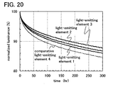
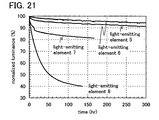
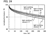
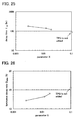
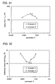
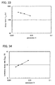
- FIG 25 is a graph in which the horizontal axis represents the parameter X and the vertical axis represents ⁇ 0.9 based on the data of Table 2.
- the lifetime of each of the light-emitting elements 1 to 3 was improved.
- the concentration of TPQ becomes higher, the value of X decreases.
- the improvement effect of lifetime can be obtained even when X is about 3 ⁇ 10 -3 .
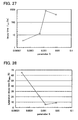
- FIG 26 is a graph in which the horizontal axis represents the parameter X and the vertical axis represents D 300hr .
- LiF lithium fluoride
Landscapes
- Physics & Mathematics (AREA)
- Optics & Photonics (AREA)
- Chemical & Material Sciences (AREA)
- Engineering & Computer Science (AREA)
- Materials Engineering (AREA)
- Spectroscopy & Molecular Physics (AREA)
- Crystallography & Structural Chemistry (AREA)
- Inorganic Chemistry (AREA)
- Electroluminescent Light Sources (AREA)
Applications Claiming Priority (1)
| Application Number | Priority Date | Filing Date | Title |
|---|---|---|---|
| JP2007340190 | 2007-12-28 |
Publications (2)
| Publication Number | Publication Date |
|---|---|
| EP2075860A2 true EP2075860A2 (de) | 2009-07-01 |
| EP2075860A3 EP2075860A3 (de) | 2013-03-20 |
Family
ID=40386447
Family Applications (1)
| Application Number | Title | Priority Date | Filing Date |
|---|---|---|---|
| EP08021477A Withdrawn EP2075860A3 (de) | 2007-12-28 | 2008-12-10 | Lichtemittierendes Element, lichtemittierende Vorrichtung und elektronische Vorrichtung |
Country Status (6)
| Country | Link |
|---|---|
| US (1) | US8203262B2 (de) |
| EP (1) | EP2075860A3 (de) |
| JP (1) | JP5358174B2 (de) |
| KR (1) | KR101608676B1 (de) |
| CN (1) | CN101692482B (de) |
| TW (1) | TWI481090B (de) |
Cited By (2)
| Publication number | Priority date | Publication date | Assignee | Title |
|---|---|---|---|---|
| US9099682B2 (en) | 2009-09-07 | 2015-08-04 | Semiconductor Energy Laboratory Co., Ltd. | Light-emitting element, light-emitting device, lighting device, and electronic device |
| EP3174118A1 (de) * | 2015-11-19 | 2017-05-31 | LG Display Co., Ltd. | Organische lichtemittierende anzeigevorrichtung |
Families Citing this family (29)
| Publication number | Priority date | Publication date | Assignee | Title |
|---|---|---|---|---|
| US7902742B2 (en) * | 2006-07-04 | 2011-03-08 | Semiconductor Energy Laboratory Co., Ltd. | Light-emitting element, light-emitting device, and electronic device |
| EP1876658A3 (de) | 2006-07-04 | 2014-06-25 | Semiconductor Energy Laboratory Co., Ltd. | Lichtemittierendes Element, lichtemittierende Vorrichtung und elektronische Vorrichtung |
| EP2091097A3 (de) * | 2008-02-13 | 2013-05-15 | Semiconductor Energy Laboratory Co, Ltd. | Lichtemittierendes Element, lichtemittierende Vorrichtung und elektronische Vorrichtung |
| WO2009116547A1 (en) * | 2008-03-18 | 2009-09-24 | Semiconductor Energy Laboratory Co., Ltd. | Light-emitting element, light-emitting device and electronic device |
| WO2009116605A1 (en) | 2008-03-18 | 2009-09-24 | Semiconductor Energy Laboratory Co., Ltd. | Light-emitting element, light-emitting device and electronic device |
| KR20140069342A (ko) | 2008-05-16 | 2014-06-09 | 가부시키가이샤 한도오따이 에네루기 켄큐쇼 | 발광소자 및 전자기기 |
| KR101596226B1 (ko) * | 2008-09-05 | 2016-02-22 | 가부시키가이샤 한도오따이 에네루기 켄큐쇼 | 발광 소자, 발광 장치 및 전자기기 |
| GB0906554D0 (en) * | 2009-04-16 | 2009-05-20 | Cambridge Display Tech Ltd | Organic electroluminescent device |
| TWI402259B (zh) * | 2009-08-28 | 2013-07-21 | Ind Tech Res Inst | 喹啉衍生物及包含此喹啉衍生物之有機發光二極體 |
| US8486544B2 (en) | 2009-08-28 | 2013-07-16 | Industrial Technology Research Institute | Quinoxaline derivatives and organic light-emitting diodes comprising the same |
| CN102484923B (zh) * | 2009-09-04 | 2016-05-04 | 株式会社半导体能源研究所 | 发光元件、发光装置及其制造方法 |
| JP2011139044A (ja) | 2009-12-01 | 2011-07-14 | Semiconductor Energy Lab Co Ltd | 発光素子、発光装置、電子機器、および照明装置 |
| EP2365556B1 (de) | 2010-03-08 | 2014-07-23 | Semiconductor Energy Laboratory Co., Ltd. | Lichtemittierendes Element, lichtemittierende Vorrichtung, elektronische Vorrichtung und Beleuchtungsvorrichtung |
| CN102201541B (zh) * | 2010-03-23 | 2015-11-25 | 株式会社半导体能源研究所 | 发光元件、发光装置、电子设备及照明装置 |
| TWI506121B (zh) | 2010-03-31 | 2015-11-01 | Semiconductor Energy Lab | 發光元件,發光裝置,電子裝置以及照明裝置 |
| JP5801579B2 (ja) | 2010-03-31 | 2015-10-28 | 株式会社半導体エネルギー研究所 | 発光素子、発光装置、電子機器、及び照明装置 |
| JP2011249319A (ja) | 2010-04-27 | 2011-12-08 | Semiconductor Energy Lab Co Ltd | 発光装置 |
| WO2011162105A1 (en) | 2010-06-25 | 2011-12-29 | Semiconductor Energy Laboratory Co., Ltd. | Light-emitting element, light-emitting device, display, and electronic device |
| DE102013214661B4 (de) * | 2012-08-03 | 2023-01-05 | Semiconductor Energy Laboratory Co., Ltd. | Licht emittierendes Element, Licht emittierende Vorrichtung und Beleuchtungsvorrichtung |
| KR102017743B1 (ko) * | 2013-01-04 | 2019-09-04 | 삼성디스플레이 주식회사 | 개선된 효율 특성을 갖는 유기 발광 소자 및 이를 포함하는 유기 발광 표시 장치 |
| KR102114878B1 (ko) * | 2014-02-27 | 2020-05-26 | 삼성디스플레이 주식회사 | 유기 발광 표시 장치 |
| KR102623039B1 (ko) | 2015-05-15 | 2024-01-08 | 가부시키가이샤 한도오따이 에네루기 켄큐쇼 | 발광 소자, 발광 장치, 전자 기기 및 조명 장치 |
| TWI564294B (zh) | 2015-08-24 | 2017-01-01 | 國立清華大學 | 載子產生材料與有機發光二極體 |
| US10270041B2 (en) | 2015-08-28 | 2019-04-23 | Semiconductor Energy Laboratory Co., Ltd. | Light-emitting element, light-emitting device, electronic device, and lighting device |
| KR102574052B1 (ko) | 2015-11-19 | 2023-09-04 | 엘지디스플레이 주식회사 | 유기발광 표시장치 |
| KR20260025923A (ko) | 2015-12-17 | 2026-02-24 | 가부시키가이샤 한도오따이 에네루기 켄큐쇼 | 발광 소자, 발광 장치, 전자 기기, 조명 장치, 조명 시스템, 및 유도 시스템 |
| US10388900B2 (en) | 2016-07-28 | 2019-08-20 | Semiconductor Energy Laboratory Co., Ltd. | Light-emitting element, light-emitting device, electronic device, and lighting device |
| US10748497B2 (en) * | 2016-12-27 | 2020-08-18 | Semiconductor Energy Laboratory Co., Ltd. | Light-emitting element, light-emitting device, electronic device, and lighting device |
| KR102701648B1 (ko) | 2016-12-28 | 2024-09-03 | 가부시키가이샤 한도오따이 에네루기 켄큐쇼 | 유기 화합물, 발광 소자, 발광 장치, 전자 기기, 표시 장치, 및 조명 장치 |
Citations (3)
| Publication number | Priority date | Publication date | Assignee | Title |
|---|---|---|---|---|
| WO2006093171A1 (en) * | 2005-02-28 | 2006-09-08 | Semiconductor Energy Laboratory Co., Ltd. | Composite material, light emitting element, light emitting device and electronic appliance using the composite material |
| US20070278937A1 (en) * | 2006-06-05 | 2007-12-06 | Stephen Forrest | Organic light-emitting device with a phosphor-sensitized fluorescent emission layer |
| US7701131B2 (en) * | 2003-07-21 | 2010-04-20 | Merck Patent Gmbh | Organic electroluminescent element comprising a carbonyl matrix material |
Family Cites Families (44)
| Publication number | Priority date | Publication date | Assignee | Title |
|---|---|---|---|---|
| DE3420039A1 (de) * | 1984-05-29 | 1985-12-12 | Hoechst Ag, 6230 Frankfurt | 2,3-bis(dialkylaminophenyl)chinoxaline und ihre verwendung in elektrophotographischen aufzeichnungsmaterialien |
| JPH06207169A (ja) | 1992-11-17 | 1994-07-26 | Idemitsu Kosan Co Ltd | 有機エレクトロルミネッセンス素子 |
| JPH0726255A (ja) | 1993-07-13 | 1995-01-27 | Idemitsu Kosan Co Ltd | 有機el素子 |
| JP2795194B2 (ja) * | 1994-09-22 | 1998-09-10 | 株式会社デンソー | エレクトロルミネッセンス素子とその製造方法 |
| DE19500912A1 (de) * | 1995-01-13 | 1996-07-18 | Basf Ag | Elektrolumineszierende Anordnung |
| JP3949214B2 (ja) * | 1997-03-18 | 2007-07-25 | 出光興産株式会社 | 有機エレクトロルミネッセンス素子 |
| JP3525034B2 (ja) * | 1997-07-31 | 2004-05-10 | 出光興産株式会社 | 有機エレクトロルミネッセンス素子 |
| JP3266573B2 (ja) * | 1998-04-08 | 2002-03-18 | 出光興産株式会社 | 有機エレクトロルミネッセンス素子 |
| JP3370011B2 (ja) * | 1998-05-19 | 2003-01-27 | 三洋電機株式会社 | 有機エレクトロルミネッセンス素子 |
| JP2000068057A (ja) | 1998-06-12 | 2000-03-03 | Idemitsu Kosan Co Ltd | 有機エレクトロルミネッセンス素子 |
| JP3287344B2 (ja) * | 1998-10-09 | 2002-06-04 | 株式会社デンソー | 有機el素子 |
| JP4024009B2 (ja) * | 2000-04-21 | 2007-12-19 | Tdk株式会社 | 有機el素子 |
| TW582121B (en) * | 2001-02-08 | 2004-04-01 | Semiconductor Energy Lab | Light emitting device |
| US6734457B2 (en) * | 2001-11-27 | 2004-05-11 | Semiconductor Energy Laboratory Co., Ltd. | Light emitting device |
| SG142163A1 (en) * | 2001-12-05 | 2008-05-28 | Semiconductor Energy Lab | Organic semiconductor element |
| EP1388903B1 (de) * | 2002-08-09 | 2016-03-16 | Semiconductor Energy Laboratory Co., Ltd. | Organische elektrolumineszente Vorrichtung |
| JP4287198B2 (ja) * | 2002-11-18 | 2009-07-01 | 出光興産株式会社 | 有機エレクトロルミネッセンス素子 |
| KR101201696B1 (ko) * | 2002-12-26 | 2012-11-15 | 가부시키가이샤 한도오따이 에네루기 켄큐쇼 | 발광 장치 |
| US6833201B2 (en) * | 2003-01-31 | 2004-12-21 | Clemson University | Nanostructured-doped compound for use in an EL element |
| JP2004273163A (ja) | 2003-03-05 | 2004-09-30 | Sony Corp | 有機el素子とその製造方法および有機elパネル |
| CN102386330B (zh) * | 2003-04-18 | 2014-10-22 | 株式会社半导体能源研究所 | 喹喔啉衍生物以及使用它的有机半导体元件、电致发光元件以及电子仪器 |
| WO2005009979A1 (ja) * | 2003-07-28 | 2005-02-03 | Semiconductor Energy Laboratory Co., Ltd. | キノキサリン誘導体及びそれを用いた発光素子 |
| CN1610468A (zh) * | 2003-10-24 | 2005-04-27 | 宾得株式会社 | 白色的有机电致发光装置 |
| JP2005310742A (ja) * | 2004-03-25 | 2005-11-04 | Sanyo Electric Co Ltd | 有機エレクトロルミネッセンス素子 |
| JP4947909B2 (ja) * | 2004-03-25 | 2012-06-06 | 三洋電機株式会社 | 有機エレクトロルミネッセンス素子 |
| US7622200B2 (en) * | 2004-05-21 | 2009-11-24 | Semiconductor Energy Laboratory Co., Ltd. | Light emitting element |
| JP4916137B2 (ja) * | 2004-07-29 | 2012-04-11 | 三洋電機株式会社 | 有機エレクトロルミネッセンス素子 |
| KR100759548B1 (ko) * | 2004-10-15 | 2007-09-18 | 삼성에스디아이 주식회사 | 유기 전계 발광 소자 |
| KR101210858B1 (ko) | 2004-11-05 | 2012-12-11 | 가부시키가이샤 한도오따이 에네루기 켄큐쇼 | 발광 소자 및 이를 이용하는 발광 장치 |
| US7892657B2 (en) * | 2004-11-30 | 2011-02-22 | Semiconductor Energy Laboratory Co., Ltd. | Light emitting element, light emitting device, and electronic device |
| JP4653469B2 (ja) * | 2004-12-01 | 2011-03-16 | 出光興産株式会社 | 有機電界発光素子 |
| JP2006253444A (ja) | 2005-03-11 | 2006-09-21 | Seiko Epson Corp | 発光装置、発光装置の製造方法、電子機器 |
| TWI307250B (en) * | 2005-03-23 | 2009-03-01 | Au Optronics Corp | Organic electroluminescent device |
| JP2006328223A (ja) * | 2005-05-26 | 2006-12-07 | Fuji Xerox Co Ltd | 高分子有機電子材料の製造方法、高分子有機電子材料及び有機電界発光素子 |
| US8592052B2 (en) | 2005-12-16 | 2013-11-26 | Mitsubishi Chemical Corporation | Organic electroluminescence device |
| EP1863105B1 (de) * | 2006-06-02 | 2020-02-19 | Semiconductor Energy Laboratory Co., Ltd. | Lichtemittierendes Element, lichtemittierende Vorrichtung und elektronische Vorrichtung |
| EP1876658A3 (de) * | 2006-07-04 | 2014-06-25 | Semiconductor Energy Laboratory Co., Ltd. | Lichtemittierendes Element, lichtemittierende Vorrichtung und elektronische Vorrichtung |
| US7902742B2 (en) * | 2006-07-04 | 2011-03-08 | Semiconductor Energy Laboratory Co., Ltd. | Light-emitting element, light-emitting device, and electronic device |
| US7911135B2 (en) * | 2006-11-29 | 2011-03-22 | Semiconductor Energy Laboratory Co., Ltd. | Light-emitting element, light emitting device, electronic appliance, and method of manufacturing the same |
| KR101435503B1 (ko) * | 2006-11-30 | 2014-08-29 | 가부시키가이샤 한도오따이 에네루기 켄큐쇼 | 발광 장치 |
| KR101426717B1 (ko) * | 2006-12-04 | 2014-08-06 | 가부시키가이샤 한도오따이 에네루기 켄큐쇼 | 발광 소자, 발광 장치 및 전자 기기 |
| KR101596676B1 (ko) * | 2007-02-21 | 2016-02-23 | 가부시키가이샤 한도오따이 에네루기 켄큐쇼 | 발광 소자, 발광 장치, 전자 기기 및 퀴녹살린 유도체 |
| EP1973386B8 (de) * | 2007-03-23 | 2016-01-13 | Semiconductor Energy Laboratory Co., Ltd. | Lichtemittierende vorrichtung und elektronische vorrichtung |
| EP2091097A3 (de) * | 2008-02-13 | 2013-05-15 | Semiconductor Energy Laboratory Co, Ltd. | Lichtemittierendes Element, lichtemittierende Vorrichtung und elektronische Vorrichtung |
-
2008
- 2008-12-10 EP EP08021477A patent/EP2075860A3/de not_active Withdrawn
- 2008-12-19 US US12/339,517 patent/US8203262B2/en not_active Expired - Fee Related
- 2008-12-23 KR KR1020080132063A patent/KR101608676B1/ko not_active Expired - Fee Related
- 2008-12-23 JP JP2008326705A patent/JP5358174B2/ja not_active Expired - Fee Related
- 2008-12-24 TW TW097150460A patent/TWI481090B/zh not_active IP Right Cessation
- 2008-12-26 CN CN2008101906982A patent/CN101692482B/zh not_active Expired - Fee Related
Patent Citations (3)
| Publication number | Priority date | Publication date | Assignee | Title |
|---|---|---|---|---|
| US7701131B2 (en) * | 2003-07-21 | 2010-04-20 | Merck Patent Gmbh | Organic electroluminescent element comprising a carbonyl matrix material |
| WO2006093171A1 (en) * | 2005-02-28 | 2006-09-08 | Semiconductor Energy Laboratory Co., Ltd. | Composite material, light emitting element, light emitting device and electronic appliance using the composite material |
| US20070278937A1 (en) * | 2006-06-05 | 2007-12-06 | Stephen Forrest | Organic light-emitting device with a phosphor-sensitized fluorescent emission layer |
Non-Patent Citations (3)
| Title |
|---|
| CHRISTIAN R. GOLDSMITH ET AL., J. AM. CHEM. SOC., vol. 124, no. 1, 2002, pages 83 - 96 |
| TETSUO TSUTSUI, JAPANESE JOURNAL OF APPLIED PHYSICS, vol. 38, 1999, pages L1502 - L1504 |
| TOSHIHIRO OHNISHI; TAMAMI KOYAMA, HIGH MOLECULAR EL MATERIAL, pages 64 - 67 |
Cited By (5)
| Publication number | Priority date | Publication date | Assignee | Title |
|---|---|---|---|---|
| US9099682B2 (en) | 2009-09-07 | 2015-08-04 | Semiconductor Energy Laboratory Co., Ltd. | Light-emitting element, light-emitting device, lighting device, and electronic device |
| US9917259B2 (en) | 2009-09-07 | 2018-03-13 | Semiconductor Energy Laboratory Co., Ltd. | Light-emitting element, light-emitting device, lighting device, and electronic device |
| EP3174118A1 (de) * | 2015-11-19 | 2017-05-31 | LG Display Co., Ltd. | Organische lichtemittierende anzeigevorrichtung |
| EP3176846A1 (de) * | 2015-11-19 | 2017-06-07 | LG Display Co., Ltd. | Organische lichtemittierende anzeigevorrichtung |
| EP4199680A1 (de) * | 2015-11-19 | 2023-06-21 | LG Display Co., Ltd. | Organische lichtemittierende anzeigevorrichtung |
Also Published As
| Publication number | Publication date |
|---|---|
| TW200945646A (en) | 2009-11-01 |
| US20090167168A1 (en) | 2009-07-02 |
| JP2009177157A (ja) | 2009-08-06 |
| KR20090072989A (ko) | 2009-07-02 |
| EP2075860A3 (de) | 2013-03-20 |
| CN101692482B (zh) | 2012-06-27 |
| US8203262B2 (en) | 2012-06-19 |
| KR101608676B1 (ko) | 2016-04-04 |
| TWI481090B (zh) | 2015-04-11 |
| CN101692482A (zh) | 2010-04-07 |
| JP5358174B2 (ja) | 2013-12-04 |
Similar Documents
| Publication | Publication Date | Title |
|---|---|---|
| EP2075860A2 (de) | Lichtemittierendes Element, lichtemittierende Vorrichtung und elektronische Vorrichtung | |
| EP2091097A2 (de) | Lichtemittierendes Element, lichtemittierende Vorrichtung und elektronische Vorrichtung | |
| US10193097B2 (en) | Light-emitting element, light-emitting device, and electronic device | |
| EP2474204B1 (de) | Lichtemittierende vorrichtung | |
| US8314548B2 (en) | Light-emitting element, light-emitting device, and electronic device | |
| CN102255054B (zh) | 发光元件、发光装置和电子装置 | |
| EP2045847A2 (de) | Lichtemittierendes Element, lichtemittierende Vorrichtung und elektronisches Gerät | |
| US8187730B2 (en) | Acenaphthoquinoxaline derivative, light-emitting element, light-emitting device, and electronic device | |
| WO2008069153A1 (en) | Light-emitting element, light-emitting device, and electronic device |
Legal Events
| Date | Code | Title | Description |
|---|---|---|---|
| PUAI | Public reference made under article 153(3) epc to a published international application that has entered the european phase |
Free format text: ORIGINAL CODE: 0009012 |
|
| AK | Designated contracting states |
Kind code of ref document: A2 Designated state(s): AT BE BG CH CY CZ DE DK EE ES FI FR GB GR HR HU IE IS IT LI LT LU LV MC MT NL NO PL PT RO SE SI SK TR |
|
| AX | Request for extension of the european patent |
Extension state: AL BA MK RS |
|
| PUAL | Search report despatched |
Free format text: ORIGINAL CODE: 0009013 |
|
| AK | Designated contracting states |
Kind code of ref document: A3 Designated state(s): AT BE BG CH CY CZ DE DK EE ES FI FR GB GR HR HU IE IS IT LI LT LU LV MC MT NL NO PL PT RO SE SI SK TR |
|
| AX | Request for extension of the european patent |
Extension state: AL BA MK RS |
|
| RIC1 | Information provided on ipc code assigned before grant |
Ipc: H01L 51/54 20060101AFI20130211BHEP Ipc: H01L 51/50 20060101ALI20130211BHEP |
|
| 17P | Request for examination filed |
Effective date: 20130903 |
|
| RBV | Designated contracting states (corrected) |
Designated state(s): AT BE BG CH CY CZ DE DK EE ES FI FR GB GR HR HU IE IS IT LI LT LU LV MC MT NL NO PL PT RO SE SI SK TR |
|
| 17Q | First examination report despatched |
Effective date: 20131018 |
|
| AKX | Designation fees paid |
Designated state(s): DE FI FR GB NL |
|
| RIC1 | Information provided on ipc code assigned before grant |
Ipc: H01L 51/52 20060101ALI20170921BHEP Ipc: H01L 51/54 20060101AFI20170921BHEP |
|
| GRAP | Despatch of communication of intention to grant a patent |
Free format text: ORIGINAL CODE: EPIDOSNIGR1 |
|
| INTG | Intention to grant announced |
Effective date: 20171027 |
|
| STAA | Information on the status of an ep patent application or granted ep patent |
Free format text: STATUS: THE APPLICATION IS DEEMED TO BE WITHDRAWN |
|
| 18D | Application deemed to be withdrawn |
Effective date: 20180307 |