EP2076960B1 - Integrierte schaltungstechnologie verwendender mikrowellenoszillator - Google Patents
Integrierte schaltungstechnologie verwendender mikrowellenoszillator Download PDFInfo
- Publication number
- EP2076960B1 EP2076960B1 EP07802915.4A EP07802915A EP2076960B1 EP 2076960 B1 EP2076960 B1 EP 2076960B1 EP 07802915 A EP07802915 A EP 07802915A EP 2076960 B1 EP2076960 B1 EP 2076960B1
- Authority
- EP
- European Patent Office
- Prior art keywords
- oscillator
- voltage
- function
- vco
- frequency
- Prior art date
- Legal status (The legal status is an assumption and is not a legal conclusion. Google has not performed a legal analysis and makes no representation as to the accuracy of the status listed.)
- Active
Links
Images

Classifications
-
- H—ELECTRICITY
- H03—ELECTRONIC CIRCUITRY
- H03C—MODULATION
- H03C3/00—Angle modulation
- H03C3/02—Details
- H03C3/08—Modifications of modulator to linearise modulation, e.g. by feedback, and clearly applicable to more than one type of modulator
Definitions
- the invention relates to a microwave oscillator in integrated circuit technology and in particular the English-language MMICs "Monolithic Microwave Integrated Circuit" operating in frequency ranges between 1GHz and 100GHz.
- Integrated microwave oscillators are used for many applications in telecommunications, radar and especially in the field of automotive radars.
- a radar sends a microwave that is reflected by one or more targets whose distances and speeds can be deduced from the delays and phase variations measured on the reflected signal.
- Sensitivity is a fundamental performance for radar, especially for automotive applications. This sensitivity is defined as the ability to detect distant targets (or weak radar surface area) as well as the ability to discriminate targets close to each other.
- the spectrum of the return signal of the radar is as narrow as possible around its emission frequency, or expressed otherwise, the bandwidth of the signal at -3 dB must be as low as possible.
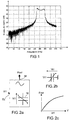
- the figure 1 represents the spectrum of a signal received in baseband (demodulated) by a radar of the state of the art without any device for servoing or precorrecting its transmission frequency.
- the relative level in dB of the received signal and on the absc issa the frequency F in kHz.
- the bandwidth is important on the order of 80 kHz to -3 dB relative to the maximum power of the received signal. Such bandwidth is incompatible with the sensitivity required for target discrimination.
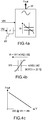
- the figure 2a shows a simplified diagram of a voltage-controlled oscillator also designated by the acronym VCO, in English "voltage controled oscillator".
- the VCO comprises an output Sf of microwave oscillation of frequency F out and a control input Ec of the frequency of the VCO.
- the change of the frequency F out of the VCO is obtained by the evolution of the capacity of a varactor 10 integrated in the VCO.
- the variation of the control voltage Vt1 applied to the varactor, by the control input Ec of the VCO, causes a modification of the capacitance of the varactor and therefore of the resonance frequency of the VCO.
- the figure 2b shows an equivalent diagram of the varactor 10 of the oscillation circuit of the VCO of the figure 2a .
- the scheme is equivalent to that of a variable capacity as a function of a control voltage Vt1 applied to its terminals.
- the Figure 2c illustrates the variation of the frequency of the VCO (F out ) as a function of the control voltage Vt1 applied to the varactor 10 of the figure 2a .
- This variation is non-linear, which has the disadvantage of reducing the sensitivity of the radar.
- the oscillator of an automobile radar is frequency-controlled by a control input ensuring a change in the emission frequency of the oscillator but also for effecting a modulation of the emission frequency around a center frequency Fc.
- a document US 2002/0089387 A1 describes a voltage controlled oscillator for frequency modulation.
- a main objective of the invention is to improve the linearity of the voltage controlled oscillator.
- the solution proposed by the invention is based on the addition of a nonlinear analog integrated system on the MMIC.
- This solution increases the linearity of the frequency variation as a function of a control voltage intended to modulate the emission, and thus improves the sensitivity of the radar.
- a voltage controlled oscillator is linear when its output frequency is proportional to its control voltage. Moreover the oscillator thus produced retains another standard control voltage for setting the central operating frequency.
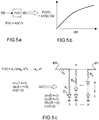
- the figure 3a shows a realization of a VCO including, as in the VCO of the figure 2a , the output Sf of microwave oscillation of frequency F out and a control input Ec1 of the frequency of the VCO and according to a main characteristic of the invention, a second input Ec2 for the application to the VCO of a second control signal Vt2.
- the change of the frequency F out of the VCO is obtained under the effect of the variation of the control voltage Vt applied to the varactor (10) of the VCO.
- k is a parameter between 0 and 1, selected according to the application.
- the value of k can, for example, be obtained by a simple voltage divider bridge.
- the figure 3b shows such a voltage divider bridge for obtaining the parameter k having two resistors R1 and R2 in series, the voltage k.Vt2 is obtained at the connection point of the two series resistors R1, R2.
- the figure 3c shows the voltage Vt applied across the capacitance of the VCO varactor of the figure 3a , the voltage Vt1 at one of the terminals and the voltage k.Vt2 at the other terminal of the capacity of the varactor.
- the figure 3d shows the variation of the oscillation frequency of the VCO (F out ) as a function of the voltage Vt1 for a constant voltage Vt2. It is found that this variation is similar to that of the state of the art VCO of the figure 2a . Therefore this configuration with two control voltages Vt1 and Vt2 does not disturb the operation described for the VCO of the state of the art of the figure 2a . This also allows to keep a wide range of frequency operation.
- the figure 3e shows the variation of oscillation frequency F out at the output of the VCO as a function of the second control voltage Vt2 for the first constant control voltage Vt1.
- This device provides a wide range of operation for the radar as a function of Vt1, and a mode of operation as a function of Vt2 more suitable for frequency modulation of the radar.
- the figure 4a shows a realization of the VCO according to the invention.
- k is a function of the second voltage Vt2, denoted k (Vt2), the value of this function being between 0 and 1.
- Vt2 the second voltage
- Vt2 the value of this function being between 0 and 1.
- the figure 4b shows the voltage Vt applied across the capacitance of the VCO varactor of the figure 4a , the voltage Vt1 at one of the terminals and the voltage k (Vt2) .Vt2 at the other terminal of the capacitance of the varactor.
- the whole of the invention is used in this embodiment of the figure 4a . with the addition of the second control voltage Vt2 through the function F.
- the function k depends in this other embodiment of the voltage Vt2.
- the figure 4c shows the frequency variation of the VCO of the figure 4a F out according to the second voltage Vt2 applied to the varactor with Vt1 constant.
- This voltage-controlled oscillator always provides a wide range of operation for the radar as a function of Vt1, and an operating mode as a function of Vt2 even more suitable for modulating the frequency of the radar, since having a increased linearity from F (Vt2) to constant Vt1. This directly improves the sensitivity of the radar without adding external compensation to the VCO.
- the function F is typically nonlinear.
- the figure 5c shows a practical realization of the function F from linear elements like resistors, and nonlinear elements like diodes.
- the rank network i comprises a resistance Ri in series with i diodes D and so on.
- the number of diodes D in a network may be different from the rank of the network.
- the network of rank i may comprise a resistor Ri in series with j diodes D.
- the function can also be performed from any element having a non-linear behavior of its current as a function of the voltage applied to it (for example transistors, etc.).
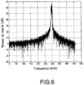
- the figure 6 shows the spectrum of the signal received in baseband (demodulated) by a radar comprising a VCO according to the invention to be compared to the spectrum of the signal of the figure 1 of a radar not including such a VCO.
- the -3 dB bandwidth of the maximum power of the signal received by the radar comprising the VCO according to the invention is 10 kHz to be compared with that of the radar of the state of the art which has a much wider width of the radar. order of 80kHz.
Landscapes
- Radar Systems Or Details Thereof (AREA)
- Inductance-Capacitance Distribution Constants And Capacitance-Resistance Oscillators (AREA)
- Stabilization Of Oscillater, Synchronisation, Frequency Synthesizers (AREA)
Claims (4)
- Integrierte Schaltungstechnologie verwendender Mikrowellenoszillator, wobei der Oszillator einen Mikrowellenausgang (Sf) besitzt, welcher eine Oszillationsfrequenz Fout als Funktion eines Steuersignals Vt besitzt, wobei die Änderung der Frequenz Fout des Oszillators unter Einwirkung der Variation der Steuerspannung Vt, welche an einen Varaktor (10) des Oszillators (VCO) angelegt wird, erzielt wird,
dadurch gekennzeichnet, dass die Oszillationsfrequenz Fout um eine Mittelfrequenz Fc über zwei Steuereingänge des Oszillators moduliert werden kann, wobei der Oszillator einen ersten Steuereingang Ec1 besitzt, welcher durch ein erstes Steuersignal Vt1 angesprochen wird, welches die Mittelfrequenz Fc des Oszillators festlegt, und einen zweiten Steuereingang Ec2, welcher durch ein zweites Steuersignal Vt2 angesprochen wird, welches die lineare Modulation dieser Mittelfrequenz Fc ermöglicht, wobei das Steuersignal Vt des Oszillators eine Funktion der beiden Steuersignale Vt1 und Vt2 ist, wobei das Steuersignal Vt, welches an den Varaktor des Oszillators angelegt wird, aus folgender Summe resultiert:
wobei k eine Funktion des zweiten Signals Vt2 ist, ausgedrückt durch k(Vt2), wobei das Steuersignal Vt dann wie folgt lautet:
wobei die Funktion F anhand der zweiten Steuerspannung Vt2 die Spannung F(Vt2) = k(Vt2).Vt2 erzeugt. - Oszillator nach Anspruch 1, dadurch gekennzeichnet, dass die Funktion F anhand von linearen Elementen wie Widerständen (R0, R1, R2,...Rp) und von nichtlinearen Elementen wie Dioden (D) oder Transistoren ausgeführt wird.
- Oszillator nach einem der vorhergehenden Ansprüche, dadurch gekennzeichnet, dass in einem gegebenen und endlichen Bereich von Steuerspannungen Vt2 die Spannung F(Vt2) durch folgende Serie beschrieben werden kann:
 wobei n ∈ {1;+∝}ai ∈ {-∝;+∝}i ∈ {1;n}wobei n und i positive Ganzzahlen sind. ai ist eine reelle Zahl.
 - Oszillator nach Anspruch 3, dadurch gekennzeichnet, dass die Funktion F durch einen Vierpol ausgeführt wird, welcher Folgendes beinhaltet:- einen Eingang Ef1 und einen Ausgang Sf1, welche durch einen Widerstand R0 verbunden sind, wobei der Ausgang Sf1 mit einem Referenzpotenzial verbunden ist, beispielsweise einer Masse M, parallel durch p Netze (0, 1, 2, ..i,...p), wobei jedes der Netze einen Widerstand R1, R2, R3,...Ri,....Rp in Reihe mit einer Anzahl j von Dioden D beinhaltet, wobei j zwischen 0 und q beträgt, wobeip ∈ {1;+∝}q ∈ {0;+∝}Ri ∈ {0;+∝}i ∈ {0;p}j ∈ {0;q}p, q, i, j positive Ganzzahlen sind. Ri ist eine positive reelle Zahl.
Applications Claiming Priority (2)
| Application Number | Priority Date | Filing Date | Title |
|---|---|---|---|
| FR0607963A FR2905808B1 (fr) | 2006-09-12 | 2006-09-12 | Oscillateur hyperfrequence en technologie des circuits integres |
| PCT/EP2007/058876 WO2008031717A2 (fr) | 2006-09-12 | 2007-08-27 | Oscillateur hyperfréquence en technologie des circuits intégrés |
Publications (2)
| Publication Number | Publication Date |
|---|---|
| EP2076960A2 EP2076960A2 (de) | 2009-07-08 |
| EP2076960B1 true EP2076960B1 (de) | 2019-12-04 |
Family
ID=37866174
Family Applications (1)
| Application Number | Title | Priority Date | Filing Date |
|---|---|---|---|
| EP07802915.4A Active EP2076960B1 (de) | 2006-09-12 | 2007-08-27 | Integrierte schaltungstechnologie verwendender mikrowellenoszillator |
Country Status (6)
| Country | Link |
|---|---|
| US (1) | US8098108B2 (de) |
| EP (1) | EP2076960B1 (de) |
| JP (1) | JP5633066B2 (de) |
| ES (1) | ES2770331T3 (de) |
| FR (1) | FR2905808B1 (de) |
| WO (1) | WO2008031717A2 (de) |
Families Citing this family (3)
| Publication number | Priority date | Publication date | Assignee | Title |
|---|---|---|---|---|
| JP2917354B2 (ja) | 1990-01-23 | 1999-07-12 | 吉富製薬株式会社 | 殻物類の熱煮方法 |
| WO2011054403A1 (en) | 2009-11-09 | 2011-05-12 | Epcos Ag | Impedance circuit and method for signal transformation |
| CN111696952B (zh) * | 2019-03-13 | 2025-07-11 | 住友电工光电子器件创新株式会社 | 微波集成电路 |
Family Cites Families (9)
| Publication number | Priority date | Publication date | Assignee | Title |
|---|---|---|---|---|
| JPH0327115U (de) * | 1989-07-26 | 1991-03-19 | ||
| JP3184049B2 (ja) * | 1994-07-04 | 2001-07-09 | 富士通株式会社 | 変調特性を改善する為の補正回路とそれを用いた変調器及びレーダ装置 |
| CA2273814A1 (en) * | 1998-10-01 | 2000-04-01 | Osram Sylvania Inc. | Wave shaping circuit |
| JP2002043842A (ja) * | 2000-07-26 | 2002-02-08 | Oki Electric Ind Co Ltd | Lc共振回路及び電圧制御型発振回路 |
| SE0003510D0 (sv) * | 2000-09-29 | 2000-09-29 | Spirea Ab | Voltage controlled oscillator |
| DE10100113A1 (de) * | 2001-01-03 | 2002-07-18 | Infineon Technologies Ag | Spannungsgesteuerter Oszillator zur Frequenzmodulation |
| JP2002359519A (ja) * | 2001-06-01 | 2002-12-13 | Murata Mfg Co Ltd | 電圧制御発振器およびそれを用いた電子装置 |
| JP2003298349A (ja) * | 2002-04-03 | 2003-10-17 | Matsushita Electric Ind Co Ltd | 電圧制御型発振回路 |
| US20050242895A1 (en) * | 2004-04-28 | 2005-11-03 | Younes Lotfi | Voltage-controlled oscillator with four terminal varactors |
-
2006
- 2006-09-12 FR FR0607963A patent/FR2905808B1/fr not_active Expired - Fee Related
-
2007
- 2007-08-27 JP JP2009527770A patent/JP5633066B2/ja active Active
- 2007-08-27 US US12/441,078 patent/US8098108B2/en active Active
- 2007-08-27 WO PCT/EP2007/058876 patent/WO2008031717A2/fr not_active Ceased
- 2007-08-27 ES ES07802915T patent/ES2770331T3/es active Active
- 2007-08-27 EP EP07802915.4A patent/EP2076960B1/de active Active
Non-Patent Citations (1)
| Title |
|---|
| None * |
Also Published As
| Publication number | Publication date |
|---|---|
| WO2008031717A3 (fr) | 2008-09-12 |
| WO2008031717A2 (fr) | 2008-03-20 |
| FR2905808B1 (fr) | 2008-12-26 |
| US20090309669A1 (en) | 2009-12-17 |
| US8098108B2 (en) | 2012-01-17 |
| ES2770331T3 (es) | 2020-07-01 |
| FR2905808A1 (fr) | 2008-03-14 |
| EP2076960A2 (de) | 2009-07-08 |
| JP2010503353A (ja) | 2010-01-28 |
| JP5633066B2 (ja) | 2014-12-03 |
Similar Documents
| Publication | Publication Date | Title |
|---|---|---|
| EP0348283A1 (de) | Frequenzvervielfacher mit einem programmierbaren Koeffizienten | |
| EP1909386A1 (de) | Negativer kapazitiver Stromkreis für Hochfrequenzanwendungen | |
| EP0562905B1 (de) | Schaltung mit veränderlicher Verzögerung | |
| EP2339744A1 (de) | Niedrigspannungs-Mischschaltung für eine Übertragungsvorrichtung von UWB-Signalen | |
| EP2202838B1 (de) | Kompakt geschalteter MEMS-Kondensator | |
| FR2786962A1 (fr) | Antenne active a reseau de dephasage | |
| EP0775390B1 (de) | Gerät zum korrigieren der amplituden-/frequenzcharakteristik eines ein kabel durchlaufenden signals und entsprechender frequenzentzerrer | |
| FR2514598A1 (fr) | Systeme de reglage de l'accentuation d'un signal video avec possibilite de reglage automatique et manuel | |
| WO2008031717A2 (fr) | Oscillateur hyperfréquence en technologie des circuits intégrés | |
| EP0230693B1 (de) | Hochfrequenz-Differenzverstärkerstufe und Verstärker mit einer solchen Differenzverstärkerstufe | |
| EP0078188B1 (de) | Breitband-Hochfrequenzanordnung zur Erzeugung von harmonischer gerader Ordnung eines Eingangssignals und deren Verwendung in einem H.F.-System | |
| FR2468252A1 (fr) | Oscillateur | |
| EP0042641B1 (de) | Frequenzdemodulator mit einer Verzögerungsschaltung, wobei die Verzögerung von der empfangenen Frequenz abhängig ist | |
| EP0401906A1 (de) | Phasenschieber | |
| EP0017301B1 (de) | Modulator zur Frequenzverschiebung | |
| EP0347985B1 (de) | Allpasstyp-Schaltung für ultrahohe Frequenzen | |
| EP0493150A1 (de) | Einstellbare Verzögerungsanordnung | |
| EP0889619B1 (de) | FSK-Modulator mit Phasenregelschleife | |
| FR2568429A1 (fr) | Convertisseur tension-frequence utilisant un circuit monostable de grande precision et procede correspondant. | |
| EP0404630B1 (de) | Vorrichtung zum Empfang von über zwei kapazitiv gekoppelte Leitungen durchgehenden Informationen, insbesondere für Kraftfahrzeuge | |
| EP1253462A1 (de) | Optischer Sender mit einem Modulator aus einer Vielzahl von Modulationselementen | |
| FR2759508A1 (fr) | Amplificateur distribue | |
| FR3155669A1 (fr) | Oscillateur électronique à commandes indépendantes de capacités variables | |
| EP4239881A1 (de) | Verfahren zum kompensieren eines internen spannungsoffsets zwischen zwei eingängen eines verstärkers | |
| FR2542525A1 (fr) | Generateur a frequence micro-onde modulable en frequence |
Legal Events
| Date | Code | Title | Description |
|---|---|---|---|
| PUAI | Public reference made under article 153(3) epc to a published international application that has entered the european phase |
Free format text: ORIGINAL CODE: 0009012 |
|
| 17P | Request for examination filed |
Effective date: 20090311 |
|
| AK | Designated contracting states |
Kind code of ref document: A2 Designated state(s): AT BE BG CH CY CZ DE DK EE ES FI FR GB GR HU IE IS IT LI LT LU LV MC MT NL PL PT RO SE SI SK TR |
|
| AX | Request for extension of the european patent |
Extension state: AL BA HR MK RS |
|
| DAX | Request for extension of the european patent (deleted) | ||
| 17Q | First examination report despatched |
Effective date: 20140103 |
|
| RAP1 | Party data changed (applicant data changed or rights of an application transferred) |
Owner name: UNITED MONOLITHIC SEMICONDUCTORS S.A. |
|
| GRAP | Despatch of communication of intention to grant a patent |
Free format text: ORIGINAL CODE: EPIDOSNIGR1 |
|
| STAA | Information on the status of an ep patent application or granted ep patent |
Free format text: STATUS: GRANT OF PATENT IS INTENDED |
|
| INTG | Intention to grant announced |
Effective date: 20190719 |
|
| GRAS | Grant fee paid |
Free format text: ORIGINAL CODE: EPIDOSNIGR3 |
|
| GRAA | (expected) grant |
Free format text: ORIGINAL CODE: 0009210 |
|
| STAA | Information on the status of an ep patent application or granted ep patent |
Free format text: STATUS: THE PATENT HAS BEEN GRANTED |
|
| AK | Designated contracting states |
Kind code of ref document: B1 Designated state(s): AT BE BG CH CY CZ DE DK EE ES FI FR GB GR HU IE IS IT LI LT LU LV MC MT NL PL PT RO SE SI SK TR |
|
| REG | Reference to a national code |
Ref country code: GB Ref legal event code: FG4D Free format text: NOT ENGLISH |
|
| REG | Reference to a national code |
Ref country code: CH Ref legal event code: EP |
|
| REG | Reference to a national code |
Ref country code: AT Ref legal event code: REF Ref document number: 1210695 Country of ref document: AT Kind code of ref document: T Effective date: 20191215 |
|
| REG | Reference to a national code |
Ref country code: DE Ref legal event code: R096 Ref document number: 602007059577 Country of ref document: DE |
|
| REG | Reference to a national code |
Ref country code: IE Ref legal event code: FG4D Free format text: LANGUAGE OF EP DOCUMENT: FRENCH |
|
| REG | Reference to a national code |
Ref country code: NL Ref legal event code: MP Effective date: 20191204 |
|
| REG | Reference to a national code |
Ref country code: LT Ref legal event code: MG4D |
|
| PG25 | Lapsed in a contracting state [announced via postgrant information from national office to epo] |
Ref country code: LV Free format text: LAPSE BECAUSE OF FAILURE TO SUBMIT A TRANSLATION OF THE DESCRIPTION OR TO PAY THE FEE WITHIN THE PRESCRIBED TIME-LIMIT Effective date: 20191204 Ref country code: BG Free format text: LAPSE BECAUSE OF FAILURE TO SUBMIT A TRANSLATION OF THE DESCRIPTION OR TO PAY THE FEE WITHIN THE PRESCRIBED TIME-LIMIT Effective date: 20200304 Ref country code: SE Free format text: LAPSE BECAUSE OF FAILURE TO SUBMIT A TRANSLATION OF THE DESCRIPTION OR TO PAY THE FEE WITHIN THE PRESCRIBED TIME-LIMIT Effective date: 20191204 Ref country code: FI Free format text: LAPSE BECAUSE OF FAILURE TO SUBMIT A TRANSLATION OF THE DESCRIPTION OR TO PAY THE FEE WITHIN THE PRESCRIBED TIME-LIMIT Effective date: 20191204 Ref country code: GR Free format text: LAPSE BECAUSE OF FAILURE TO SUBMIT A TRANSLATION OF THE DESCRIPTION OR TO PAY THE FEE WITHIN THE PRESCRIBED TIME-LIMIT Effective date: 20200305 Ref country code: LT Free format text: LAPSE BECAUSE OF FAILURE TO SUBMIT A TRANSLATION OF THE DESCRIPTION OR TO PAY THE FEE WITHIN THE PRESCRIBED TIME-LIMIT Effective date: 20191204 |
|
| REG | Reference to a national code |
Ref country code: ES Ref legal event code: FG2A Ref document number: 2770331 Country of ref document: ES Kind code of ref document: T3 Effective date: 20200701 |
|
| PG25 | Lapsed in a contracting state [announced via postgrant information from national office to epo] |
Ref country code: RO Free format text: LAPSE BECAUSE OF FAILURE TO SUBMIT A TRANSLATION OF THE DESCRIPTION OR TO PAY THE FEE WITHIN THE PRESCRIBED TIME-LIMIT Effective date: 20191204 Ref country code: CZ Free format text: LAPSE BECAUSE OF FAILURE TO SUBMIT A TRANSLATION OF THE DESCRIPTION OR TO PAY THE FEE WITHIN THE PRESCRIBED TIME-LIMIT Effective date: 20191204 Ref country code: EE Free format text: LAPSE BECAUSE OF FAILURE TO SUBMIT A TRANSLATION OF THE DESCRIPTION OR TO PAY THE FEE WITHIN THE PRESCRIBED TIME-LIMIT Effective date: 20191204 Ref country code: PT Free format text: LAPSE BECAUSE OF FAILURE TO SUBMIT A TRANSLATION OF THE DESCRIPTION OR TO PAY THE FEE WITHIN THE PRESCRIBED TIME-LIMIT Effective date: 20200429 Ref country code: NL Free format text: LAPSE BECAUSE OF FAILURE TO SUBMIT A TRANSLATION OF THE DESCRIPTION OR TO PAY THE FEE WITHIN THE PRESCRIBED TIME-LIMIT Effective date: 20191204 |
|
| PG25 | Lapsed in a contracting state [announced via postgrant information from national office to epo] |
Ref country code: IS Free format text: LAPSE BECAUSE OF FAILURE TO SUBMIT A TRANSLATION OF THE DESCRIPTION OR TO PAY THE FEE WITHIN THE PRESCRIBED TIME-LIMIT Effective date: 20200404 Ref country code: SK Free format text: LAPSE BECAUSE OF FAILURE TO SUBMIT A TRANSLATION OF THE DESCRIPTION OR TO PAY THE FEE WITHIN THE PRESCRIBED TIME-LIMIT Effective date: 20191204 |
|
| REG | Reference to a national code |
Ref country code: DE Ref legal event code: R097 Ref document number: 602007059577 Country of ref document: DE |
|
| REG | Reference to a national code |
Ref country code: AT Ref legal event code: MK05 Ref document number: 1210695 Country of ref document: AT Kind code of ref document: T Effective date: 20191204 |
|
| PLBE | No opposition filed within time limit |
Free format text: ORIGINAL CODE: 0009261 |
|
| STAA | Information on the status of an ep patent application or granted ep patent |
Free format text: STATUS: NO OPPOSITION FILED WITHIN TIME LIMIT |
|
| PG25 | Lapsed in a contracting state [announced via postgrant information from national office to epo] |
Ref country code: DK Free format text: LAPSE BECAUSE OF FAILURE TO SUBMIT A TRANSLATION OF THE DESCRIPTION OR TO PAY THE FEE WITHIN THE PRESCRIBED TIME-LIMIT Effective date: 20191204 |
|
| 26N | No opposition filed |
Effective date: 20200907 |
|
| PG25 | Lapsed in a contracting state [announced via postgrant information from national office to epo] |
Ref country code: AT Free format text: LAPSE BECAUSE OF FAILURE TO SUBMIT A TRANSLATION OF THE DESCRIPTION OR TO PAY THE FEE WITHIN THE PRESCRIBED TIME-LIMIT Effective date: 20191204 Ref country code: PL Free format text: LAPSE BECAUSE OF FAILURE TO SUBMIT A TRANSLATION OF THE DESCRIPTION OR TO PAY THE FEE WITHIN THE PRESCRIBED TIME-LIMIT Effective date: 20191204 Ref country code: SI Free format text: LAPSE BECAUSE OF FAILURE TO SUBMIT A TRANSLATION OF THE DESCRIPTION OR TO PAY THE FEE WITHIN THE PRESCRIBED TIME-LIMIT Effective date: 20191204 |
|
| PG25 | Lapsed in a contracting state [announced via postgrant information from national office to epo] |
Ref country code: MC Free format text: LAPSE BECAUSE OF FAILURE TO SUBMIT A TRANSLATION OF THE DESCRIPTION OR TO PAY THE FEE WITHIN THE PRESCRIBED TIME-LIMIT Effective date: 20191204 |
|
| REG | Reference to a national code |
Ref country code: CH Ref legal event code: PL |
|
| PG25 | Lapsed in a contracting state [announced via postgrant information from national office to epo] |
Ref country code: CH Free format text: LAPSE BECAUSE OF NON-PAYMENT OF DUE FEES Effective date: 20200831 Ref country code: LI Free format text: LAPSE BECAUSE OF NON-PAYMENT OF DUE FEES Effective date: 20200831 Ref country code: LU Free format text: LAPSE BECAUSE OF NON-PAYMENT OF DUE FEES Effective date: 20200827 |
|
| REG | Reference to a national code |
Ref country code: BE Ref legal event code: MM Effective date: 20200831 |
|
| PG25 | Lapsed in a contracting state [announced via postgrant information from national office to epo] |
Ref country code: BE Free format text: LAPSE BECAUSE OF NON-PAYMENT OF DUE FEES Effective date: 20200831 Ref country code: IE Free format text: LAPSE BECAUSE OF NON-PAYMENT OF DUE FEES Effective date: 20200827 |
|
| PG25 | Lapsed in a contracting state [announced via postgrant information from national office to epo] |
Ref country code: TR Free format text: LAPSE BECAUSE OF FAILURE TO SUBMIT A TRANSLATION OF THE DESCRIPTION OR TO PAY THE FEE WITHIN THE PRESCRIBED TIME-LIMIT Effective date: 20191204 Ref country code: MT Free format text: LAPSE BECAUSE OF FAILURE TO SUBMIT A TRANSLATION OF THE DESCRIPTION OR TO PAY THE FEE WITHIN THE PRESCRIBED TIME-LIMIT Effective date: 20191204 Ref country code: CY Free format text: LAPSE BECAUSE OF FAILURE TO SUBMIT A TRANSLATION OF THE DESCRIPTION OR TO PAY THE FEE WITHIN THE PRESCRIBED TIME-LIMIT Effective date: 20191204 |
|
| P01 | Opt-out of the competence of the unified patent court (upc) registered |
Effective date: 20230517 |
|
| PGFP | Annual fee paid to national office [announced via postgrant information from national office to epo] |
Ref country code: ES Payment date: 20250902 Year of fee payment: 19 |
|
| PGFP | Annual fee paid to national office [announced via postgrant information from national office to epo] |
Ref country code: DE Payment date: 20250716 Year of fee payment: 19 |
|
| PGFP | Annual fee paid to national office [announced via postgrant information from national office to epo] |
Ref country code: IT Payment date: 20250728 Year of fee payment: 19 |
|
| PGFP | Annual fee paid to national office [announced via postgrant information from national office to epo] |
Ref country code: GB Payment date: 20250717 Year of fee payment: 19 |
|
| PGFP | Annual fee paid to national office [announced via postgrant information from national office to epo] |
Ref country code: FR Payment date: 20250721 Year of fee payment: 19 |