EP2079103A1 - Verfahren zur bearbeitung einer festen oberfläche mit einem gascluster-ionenstrahl - Google Patents
Verfahren zur bearbeitung einer festen oberfläche mit einem gascluster-ionenstrahl Download PDFInfo
- Publication number
- EP2079103A1 EP2079103A1 EP07831192A EP07831192A EP2079103A1 EP 2079103 A1 EP2079103 A1 EP 2079103A1 EP 07831192 A EP07831192 A EP 07831192A EP 07831192 A EP07831192 A EP 07831192A EP 2079103 A1 EP2079103 A1 EP 2079103A1
- Authority
- EP
- European Patent Office
- Prior art keywords
- cluster
- ion beam
- protection layer
- solid surface
- gas cluster
- Prior art date
- Legal status (The legal status is an assumption and is not a legal conclusion. Google has not performed a legal analysis and makes no representation as to the accuracy of the status listed.)
- Withdrawn
Links
Images


Classifications
-
- H—ELECTRICITY
- H10—SEMICONDUCTOR DEVICES; ELECTRIC SOLID-STATE DEVICES NOT OTHERWISE PROVIDED FOR
- H10P—GENERIC PROCESSES OR APPARATUS FOR THE MANUFACTURE OR TREATMENT OF DEVICES COVERED BY CLASS H10
- H10P50/00—Etching of wafers, substrates or parts of devices
-
- H—ELECTRICITY
- H10—SEMICONDUCTOR DEVICES; ELECTRIC SOLID-STATE DEVICES NOT OTHERWISE PROVIDED FOR
- H10P—GENERIC PROCESSES OR APPARATUS FOR THE MANUFACTURE OR TREATMENT OF DEVICES COVERED BY CLASS H10
- H10P50/00—Etching of wafers, substrates or parts of devices
- H10P50/69—Etching of wafers, substrates or parts of devices using masks for semiconductor materials
- H10P50/691—Etching of wafers, substrates or parts of devices using masks for semiconductor materials for Group V materials or Group III-V materials
- H10P50/693—Etching of wafers, substrates or parts of devices using masks for semiconductor materials for Group V materials or Group III-V materials characterised by their size, orientation, disposition, behaviour or shape, in horizontal or vertical plane
-
- H—ELECTRICITY
- H10—SEMICONDUCTOR DEVICES; ELECTRIC SOLID-STATE DEVICES NOT OTHERWISE PROVIDED FOR
- H10P—GENERIC PROCESSES OR APPARATUS FOR THE MANUFACTURE OR TREATMENT OF DEVICES COVERED BY CLASS H10
- H10P50/00—Etching of wafers, substrates or parts of devices
- H10P50/20—Dry etching; Plasma etching; Reactive-ion etching
- H10P50/24—Dry etching; Plasma etching; Reactive-ion etching of semiconductor materials
- H10P50/242—Dry etching; Plasma etching; Reactive-ion etching of semiconductor materials of Group IV materials
-
- H—ELECTRICITY
- H01—ELECTRIC ELEMENTS
- H01J—ELECTRIC DISCHARGE TUBES OR DISCHARGE LAMPS
- H01J2237/00—Discharge tubes exposing object to beam, e.g. for analysis treatment, etching, imaging
- H01J2237/06—Sources
- H01J2237/08—Ion sources
- H01J2237/0812—Ionized cluster beam [ICB] sources
Definitions
- the present invention relates to a method of processing a solid surface with gas cluster ion beam irradiation.
- Semiconductor devices, electronic devices, and photonic-crystal and other optical devices are fabricated by forming submicrometer (around 0.1 ⁇ m to 1 ⁇ m) precision pattern structures on a face of a semiconductor wafer and the like.
- semiconductor quantum devices an array of ultra-fine particles or lines measured in nanometers, which are called quantum dots or quantum wires, is formed on a surface of a substrate.
- the size and surface roughness of the relief structures (pattern structures, structures formed by an array of ultra-fine particles, etc.) formed on those devices are important factors that affect the performance of the devices. Therefore, high precision is essential for the formation of the relief structure.
- the precision of the relief structure depends on the precision of a film formation processes, an etching processes, and other fabrication processes. It is not easy to form a relief structure with a precision of up to a few nanometers. Generally, in these devices fabricated through the film formation process, etching process, and so on, a great number of chips are formed on the surface of a semiconductor wafer. However, it is difficult to form uniform relief structures across the entire surface of the semiconductor wafer. To solve these problems, a process to improve the precision of the structure (such as smoothing) is conducted after the relief structure is formed.
- Patent literature 1 smoothes out side walls of a pattern structure and the like by irradiating it with a gas cluster ion beam.
- Patent literature 1 uses oblique irradiation to smooth out side walls of a relief structure. Approximately perpendicular irradiation is conducted at an irradiation angle of about 0° with respect to the normal to the solid surface.
- the finding indicates that the gas cluster ion beam emitted onto the side walls of the relief structure cannot perform adequate surface processing to smooth out the exposed surface, while keeping its contour similar to the contour of the relief structure.
- an object of the present invention is to provide a method of processing a solid surface, while preventing corner portions of a relief structure from being deformed.
- a method of processing a solid surface with a gas cluster ion beam includes a cluster-protection-layer formation step of forming, on the solid surface, a relief structure having protrusions with a cluster protection layer formed to cover an upper part thereof and recesses without the cluster protection layer; an irradiation step of emitting the gas cluster ion beam onto the solid surface on which the relief structure has been formed in the cluster-protection-layer formation step; and a removal step of removing the cluster protection layer.
- the gas cluster ion beam is emitted onto the solid surface having the relief structure with the cluster protection layer formed on the upper part of the protrusions.
- the cluster-protection-layer formation step may include a masking process of forming the cluster protection layer to cover the solid surface; and an etching process of etching the solid surface having the cluster protection layer formed in the masking process, thereby forming the relief structure having the recesses reaching the solid and the protrusions with the cluster protection layer left on the upper part thereof.
- a thickness T [cm] of the cluster protection layer satisfy Equation (r1): T > nY + b 2 ⁇ Y 2 ⁇ n - n ⁇ Y 2 ⁇ b 4 - 16 ⁇ a 2 1 2 2 1 2 , where n is a dose [ions/cm 2 ] of the gas cluster ion beam; and Y is an etching efficiency of the cluster protection layer, given as an etching volume per cluster [cm 3 /ion] ( a is a proportionality factor [ions/cm 2 ] between nY 2 [cm 4 /ion] and an area S [cm 2 ] of a region of the cluster protection layer etched by the gas cluster ion beam, in a cross section perpendicular to a direction in which the protrusions or the recesses extend; and b is a proportionality factor [ions 1/2 cm -1 ] between Yn 1/2 [cm 2 ⁇ ions -1/2 ] and a length L
- Equation (r1) is a necessary and sufficient condition for the thickness of the cluster protection layer that can prevent the shape of the corner portions of the relief structure from being deformed.
- the thickness T [cm] of the cluster protection layer satisfy: T > nY + 1.54 * 10 16 * n ⁇ Y 2 1 / 2 . If an SF 6 gas cluster ion beam is used, it is preferred that the thickness T [cm] of the cluster protection layer satisfy: T > nY + 1.23 ⁇ e * 10 15 * n ⁇ Y 2 1 / 2 .
- the gas cluster ion beam may be alternately emitted obliquely onto opposite side walls of the relief structure, and the solid may be rotated on an axis approximately parallel to the normal to the solid surface on which the relief structure is formed while being irradiated with the gas cluster ion beam.
- the inventors conducted a variety of experiments and found that the lateral transfer of a substance, which is characteristic to a gas cluster ion beam (GCIB), is deeply involved in the deformation of corner portions of a relief structure by the GCIB emitted on it. As a result of thorough examination, the inventors have first succeeded in quantitatively clarifying the relationship between the GCIB irradiation conditions and the shape and amount of deformation of the corner portions and clarifying the mechanism of deformation of the corners.
- GCIB gas cluster ion beam
- the relief structure here means a pattern structure such as a line-and-space pattern of a few nanometers to submicrometers formed on a solid surface of a silicon substrate, SOI (silicon on insulator), or the like and a rise-and-fall structure such as a structure including an array of ultrafine particles such as quantum dots.
- a pattern structure such as a line-and-space pattern of a few nanometers to submicrometers formed on a solid surface of a silicon substrate, SOI (silicon on insulator), or the like and a rise-and-fall structure such as a structure including an array of ultrafine particles such as quantum dots.
- the corner portion of the relief structure is a corner portion in the upper part of the side wall of the relief structure (the wall of a protrusion which is a structure portion protruding from a solid surface or the wall of a recess which is a recessed structure portion in a solid surface).
- the upper part here is on the side far from the solid surface on which the relief structure is formed.
- the lateral transfer of a substance is the transfer of atoms in a GCIB irradiation area of the solid surface in a direction approximately parallel to the solid surface. This phenomenon contributes to the smoothing of the substrate surface.
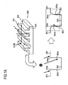
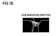
- a line-and-space pattern structure 900 is irradiated with a GCIB.
- a side wall 903 of a line of the line-and-space pattern structure 900 is irradiated with the GCIB obliquely.
- Gas cluster ions collide with corner portions 904a and 904b of lines 901 as well, causing substances forming the corner portions 904a and 904b of the lines 901 to travel laterally.
- the lateral transfer is represented by a dashed arrow in the bottom right diagram in Fig. 1A .
- the substance traveling laterally on the side wall 903 of the line toward the bottom of a space 902 runs and deposits on the side wall 903 of the line and protrudes into the space 902.
- a side wall A 903a of the line facing the incident GCIB continues to be irradiated with the GCIB, and a deposit 801 of the substance on the side wall A 903a of the line travels further laterally.
- the amount of lateral transfer in the direction of GCIB irradiation increases, causing hardly any lateral transfer toward the corner portion 904a in the upper part of the side wall A 903a of the line.
- a side wall B 903b of an adjacent line facing the side wall A 903a of the line is not irradiated with the GCIB, so that a deposit 802 on the side wall B 903b of the line does not travel laterally toward the corner portion in the upper part of the side wall B 903b of the line.
- corner portions caused by the GCIB irradiation.
- the corner portions are deformed by approximately perpendicular irradiation as well (the two side walls of a line become analogous to the side wall B of the line).
- the oblique angle of an incline portion formed per unit dose increases, increasing the amount of substance staying on the side wall of the line or the bottom of the space.
- the side wall A 903a of the line facing the incident GCIB is exposed to the GCIB more than the side wall B 903b of an adjacent line facing the side wall A 903a of the line. This difference makes the oblique angle in the upper part of the side wall A 903 a of the line greater than the oblique angle in the upper part of the side wall B 903b of the line.
- Part of the substance 801 staying on the side wall A 903a of the line is eliminated by etching and becomes less than the substance 802.
- ⁇ is the oblique angle
- L is the length of the oblique side.
- the oblique angle ⁇ is the oblique angle of the incline portion formed in the upper part of the side wall A 903a of the line facing the incident GCIB.
- the length L of the oblique side is the length of the oblique side of the incline portion formed in the upper part of the side wall A 903a of the line facing the incident GCIB (see Fig. 2 ):
- the dose [ions/cm 2 ] is represented by n
- the etching efficiency of the substance (etching volume per cluster) [cm 3 /ion] is represented by Y .
- Proportionality factors a and b are constants determined by the GCIB conditions.
- a [ions/cm 2 ] is the proportionality factor between nY 2 [cm 4 /ion] and the cross-sectional area S [cm 2 ] of the deformed corner portion
- b [ions 1/2 cm -1 ] is the proportionality factor between Yn 1/2 [cm 2 ⁇ ions -1/2 ] and the length L [cm] of the oblique side.
- the cross-sectional area S of the deformed corner portion corresponds to an area of a region (comer portion, which is a shaded portion in Fig. 2 ) etched most by the GCIB in a cross section perpendicular to the direction in which the protrusion or recess extends.
- the length L of the oblique side corresponds to the length of the oblique side of the cross section perpendicular to the direction in which the protrusion or recess extends, of a region etched most by the gas cluster ion beam.
- Equation (1) expresses that the volume of the corner portion removed by deformation per unit depth is proportional to the square of the etching efficiency Y and the dose n.
- the unit depth is the x-axis direction in Fig. 1A and is the direction in which the protrusion or recess extends.
- the volume per unit depth corresponds to the cross-sectional area S of the deformed corner portion.
- Equation (2) expresses that the length L of the oblique side is proportional to the etching efficiency Y and the square root of the dose n.
- the oblique angle ⁇ of the incline portion in the upper part of the side wall A 903 a of the line and the depth d of deformation can be predicted.
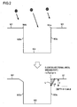
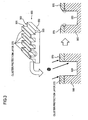
- a layer (refered to as a cluster protection layer 570) formed on the top face of a line 501 in a line-and-space pattern structure 500 by a material differing from the material of the solid 550, surface smoothing or other surface processing can be conducted on the side wall 503 of the line without deforming the corner portions of the line 501 (see Fig. 3 , especially parts circled by dashed lines in the bottom right diagram in Fig. 3 ).
- the cluster protection layer 570 is formed, the optimum thickness (such necessary and sufficient thickness that the corner portions of the line 501 will not be deformed) can be selected in accordance with Equation (6).
- Equations (3) and (4) are substituted into Equations (1) and (2) respectively; ⁇ and L are eliminated; and a simultaneous equation concerning d is obtained.
- the thickness T [cm] of the cluster protection layer 570 should satisfy Equation (6): T > nY + b 2 ⁇ Y 2 ⁇ n - n ⁇ Y 2 ⁇ b 4 - 16 ⁇ a 2 1 2 2 1 2 .
- Equations (1) and (2) are derived will be described specifically in accordance with the results of experiments using an Ar (argon) gas cluster.
- a line-and-space pattern structure was fabricated on the surface of a variety of solid materials (silicon (Si), silicon dioxide (SiO 2 ), and chromium (Cr)).
- lines and spaces have an equal width of 5 ⁇ m.
- the groove depth (line height) was 1 ⁇ m for silicon, 1 ⁇ m for silicon dioxide, and 300 nm for chromium.
- the line-and-space pattern structure was fabricated as described below. The equipment used for the fabrication will be described later.
- Fabrication on silicon was as follows. The surface of the silicon substrate was thermally oxidized to form an oxide film on the surface of the silicon substrate. The oxide film was coated with electron beam resist, and a line-and-space pattern was drawn. After the resist was developed, the resist pattern was used as a mask when the thermally oxidized film was etched. After the resist was removed, the thermally oxidized film was used as a hard mask when the silicon was etched. The thermally oxidized film was removed by ashing, and the line-and-space pattern structure was obtained.
- Fabrication on silicon dioxide was as follows. The surface of the silicon substrate was thermally oxidized to form an oxide film on the surface of the silicon substrate.
- the thermally oxidized film (SiO 2 ) was coated with electron beam resist, and a line-and-space pattern was drawn. After the resist was developed, the resist pattern was used as a mask when the thermally oxidized film was etched. The resist was removed, and the line-and-space pattern structure was obtained.
- Fabrication on chromium was as follows. The surface of the silicon substrate was coated with electron beam resist, and a line-and-space pattern was drawn. After the resist was developed, a chromium film was deposited by sputtering. The thickness of the deposited chromium film was 300 nm. The resist was removed, leaving the chromium film on a part where there was no resist (lift-off method), and the line-and-space pattern structure was obtained.
- the length L of the oblique side and the dose n were observed on silicon (Si) used as the solid material, and it was found that the length L of the oblique side was nearly proportional to n 0.5 (see Fig. 4B ).
- the relationship suggests that the lateral transfer of substance is governed by random walk. It is thought that the length L of the oblique side of the incline portion is derived from the fact that the distance of lateral transfer of atoms in the solid material is proportional to the square root of the number n of irradiation events.
- Fig. 4C is a graph showing the relationship between the length L of the oblique side and the product of the etching efficiency Y and n 0.5 of silicon, silicon dioxide, and chromium. Because the relationship L ⁇ n 0.5 had been obtained already, as described earlier, the relationship between the length L of the oblique side and the etching efficiency Y can be inferred from the relationship between the length L of the oblique side and Y*n 0.5 . It can be interpreted that most of the obtained data points are on a single straight line.
- Fig. 4D shows the relationship between the cross-sectional area S and the product of the square of the etching efficiency Y and the dose n observed on silicon, silicon dioxide, and chromium. The relationship shows that the cross sectional area S increases in proportion to n*Y 2 .
- Equations (1) and (2) were obtained.
- the values of proportionality factors a and b obtained from Figs. 4C and 4D are almost constant for any type of solid material: a ⁇ 3.80*10 16 [ions/cm 2 ]; b ⁇ 6.25*10 8 [ions 1/2 /cm -1 ].
- the values are correct to three significant figures. Accordingly, the cluster protection layer can be made of any material, and the cluster protection layer should be formed to have a thickness greater than the deformation depth d calculated from Equation (5).
- the thickness T of the cluster protection layer when the Ar gas cluster ion beam is used is obtained from Equation (7), which is obtained by substituting the values of constants a and b into Equation (6): T > nY + 1.54 * 10 16 ⁇ n ⁇ Y 2 1 / 2 , where n is the dose [ions/cm 2 ] of the gas cluster ion beam, and the etching efficiency Y is given as the etching volume per cluster ion [cm 3 /ion].
- the deformation depth d and the length L of the oblique side of the corner portion of the line were observed on a variety of materials after SF 6 gas cluster ion beam irradiation.
- the relationship between the dose n and the cross-sectional area S of the incline portion was examined on silicon used as the solid material.
- the cross-sectional area S increases in proportion to an increase in the dose n ( Fig. 5A ).
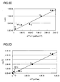
- Fig. 5C is a graph showing the relationship between the length L of the oblique side and the product of the etching efficiency Y and n 0.5 of silicon, silicon dioxide, and chromium. It can be interpreted that most of the obtained data points are on a single straight line.
- Fig. 5D shows the relationship between the cross-sectional area S of the deformed portion and the product of the square of the etching efficiency Y and the dose n, observed on silicon, silicon dioxide, and chromium.
- the obtained proportional relationship indicates that a material having a greater value of nY 2 has a linearly increasing cross-sectional area S.
- the values are correct to three significant figures. Accordingly, the cluster protection layer can be made of any material, and the cluster protection layer should be formed to have a thickness greater than the deformation depth d calculated from Equation (5).
- the thickness T of the cluster protection layer when the SF 6 gas cluster ion beam is used is obtained from Equation (8), which is obtained by substituting the values of the proportionality factors a and b into Equation (6), T > nY + 1.23 * 10 15 ⁇ n ⁇ Y 2 1 / 2 , where n is the dose [ions/cm 2 ] of the gas cluster ion beam, and the etching efficiency Y is the etching volume per cluster ion [cm 3 /ion].
- the values of a and b depend on the gas type of the gas cluster ion beam because the proportion of etching to lateral transfer of substance caused by gas cluster ion beam irradiation is different. As the accelerating energy of the gas cluster ion beam increases, both the etching efficiency and the lateral transfer of substance increase, and the proportion of them does not change greatly. Therefore, if the gas type is the same, the values of the proportionality factors a and b do not depend on the accelerating energy.
- the cluster protection layer formed on the top face of the line prevents the deformation of corner portions in the upper parts of the side walls of the line below the cluster protection layer, thus allowing surface processing (such as smoothing of the side walls of the line).
- Masking means forms a cluster protection layer to cover a solid surface.
- the masking means may be the same one as included in a general wafer processing apparatus.
- the masking means in this embodiment is a high-temperature diffusion furnace.
- a silicon substrate is placed in the high-temperature diffusion furnace and exposed to an oxidizing gas atmosphere at a high temperature (generally around 900°C to 1100°C). This forms a thermally oxidized film across the surface of the silicon substrate.
- the thermally oxidized film corresponds to the cluster protection layer.
- Etching means conducts dry etching of the solid surface on which the cluster protection layer has been formed. This forms a relief structure on the solid surface.
- the etching means can be the same one as included in a general wafer processing apparatus. In this embodiment, an etching apparatus is used. An example of etching the silicon substrate on which a thermally oxidized film is formed will be described. The etching is performed as follows. The thermally oxidized film is coated with photoresist. Prebaking is performed to adhere the thermally oxidized film to the photoresist. The photoresist is then exposed to light through a photomask, and the pattern of the photomask is printed (transferred) onto the photoresist. The exposed photoresist is then developed and rinsed.
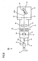
- the solid surface processing apparatus 100 includes gas cluster ion beam emission means which emits a gas cluster ion beam onto a solid surface.
- the GCIB emission means shown in Fig. 6 is structured as follows. Source gas 9 is supplied by a nozzle 10 into a vacuum cluster generation chamber 11. Gas molecules of the source gas 9 aggregate into clusters in the cluster generation chamber 11. The size of the clusters is determined by the particle size distribution based on the pressure and temperature of gas at a nozzle outlet 10a and the size and shape of the nozzle 10. The clusters generated in the cluster generation chamber 11 are brought by a skimmer 12 into an ionization chamber 13 to serve as a gas cluster beam.
- an ionizer 14 emits an electron beam, such as a thermal electron beam, and the neutral cluster is ionized.
- the ionized gas cluster beam (GCIB) is accelerated by an accelerating electrode 15, converged by a magnetic-field convergence unit 16, and input to a sputtering chamber 17.
- a target support 18 provided in the sputtering chamber 17 a target 19, which is a solid (such as a silicon substrate on which a relief structure is formed) to be exposed to the GCIB, is fixed on a rotary disc 41.
- the GCIB entering the sputtering chamber 17 is narrowed to a predetermined beam diameter by an aperture 21 and directed onto the surface of the target 19.
- the GCIB is neutralized by electron beam irradiation.
- the solid surface processing apparatus 100 includes determination means which determines whether the thickness of the cluster protection layer, the etching efficiency of the material of the cluster protection layer, and the dose of the gas cluster ion beam satisfy the relationship expressed by Equation (5).
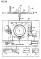
- an input unit 30 such as a keyboard is connected to the solid surface processing apparatus 100, as shown in Fig. 7B .
- the thickness of the cluster protection layer, the etching efficiency of the material of the cluster protection layer, and the dose of the gas cluster ion beam are input.
- a determination unit 27 determines whether the input thickness of the cluster protection layer, the input etching efficiency of the material of the cluster protection layer, and the input dose of the gas cluster ion beam satisfy the relationship of Equation (5) and outputs the result of the determination. The result is displayed on a display unit 26.
- the thickness of the cluster protection layer and the etching efficiency of the material of the cluster protection layer may be input through the input unit 30, and the determination unit 27 may obtain a dose of the gas cluster ion beam satisfying the relationship of Equation (5) on the basis of the input thickness of the cluster protection layer, the input etching efficiency of the material of the cluster protection layer, and Equation (5).
- the dose of the gas cluster ion beam obtained by the determination unit 27 is displayed on the display unit 26.
- the solid surface processing apparatus 100 also includes means that can set the irradiation angle to alternately and obliquely irradiate opposite side walls of the relief structure formed on the solid surface by the etching means with the GCIB (alternate irradiation means) or means that can rotate the solid on an axis approximately parallel to the normal to the solid surface to be irradiated with the GCIB (rotary irradiation means), or includes both of the means, when needed.
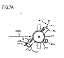
- This embodiment includes rotation mechanisms that implement the above two means.
- the solid surface processing apparatus 100 includes a first rotation mechanism and a second rotation mechanism.
- the first rotation mechanism corresponds to the rotary irradiation means and is structured as follows.
- the target support 18 has a protruding shaft 41a, and the rotary disc 41 is mounted on the shaft 41a to rotate on the center of the shaft 41a.
- the rotary disc 41 has a flat part 41b, on which the target 19 is attached.
- the rotary disc 41 has a great number of teeth in its rim 41 c, and the teeth engage with the teeth of a gear 43.
- the gear 43 rotates when driven by a motor 42, and the rotation is transferred to the rotary disc 41, thereby rotating the target 19 attached to the rotary disc 41.
- the target 19 can be rotated on a shaft almost parallel to the normal to the solid surface to be irradiated with the GCIB while the target 19 is being irradiated with the GCIB.
- the second rotation mechanism corresponds to alternate irradiation means and is structured as follows.
- a rotation shaft 21 is fixed to the target support 18, and the target support 18 can rotate on the center of the rotation shaft 21.
- the rotation shaft 21 is rotatably supported by stationary plates 22a and 22b.
- the rotation shaft 21 is fixed also to the center of the rotation axis of a gear 24b, and the gear 24b engages with a gear 24a.
- the gear 24a rotates when driven by a motor 23, and the rotation is transferred to the gear 24b and the rotation shaft 21, thereby rotating the target support 18.
- the GCIB can be emitted to the target 19 obliquely and alternately by repeating these steps:
- the target support 18 is held still in a position + ⁇ ( ⁇ expresses the magnitude of the angle of rotation); the target 19 is irradiated with the GCIB; after a predetermined period of time, the target support 18 is rotated and held still in a position - ⁇ ' ( ⁇ ' expresses the magnitude of the angle of rotation; usually, ⁇ ⁇ ⁇ '); the GCIB is emitted to the target 19; after a predetermined period of time, the target support 18 is rotated and held still in the position + ⁇ ; and the GCIB is emitted onto the target 19.
- the solid surface processing apparatus 100 is further equipped with a scanning mechanism for changing the relative position of the target 19 with respect to the GCIB, such as an XY stage.
- the stationary plates 22a and 22b are fixed to and supported by a stationary-plate supporting member 22c, as shown in Fig. 7B .
- the stationary-plate supporting member 22c and a first actuator 22d are connected via a first rod 22e.
- the first actuator 22d can push and pull the first rod 22e, and this action can change the position of the target support 18.
- the motion of the first actuator 22d can change the position of the target support 18 towards the top or bottom on the page.
- the first actuator 22d is fixed to and supported by a second rod 22g, and the first actuator 22d is connected to second actuators 22f through the second rod 22g.
- the second actuators 22f can push and pull the second rod 22g, and this action changes the position of the first actuator 22d. Consequently, the position of the target support 18 connected to the first actuator 22d via the first rod 22e and the other parts mentioned above can be changed.
- the direction in which the first rod 22e can move is nearly orthogonal to the direction in which the second rod 22g can move. In that way, a scanning mechanism like an XY stage is implemented.
- the motion of the second actuators 22f can change the position of the target support 18 towards the left or right on the page. Therefore, in combination with the motion of the first actuator 22d, the target support 18 can be moved up and down, and left and right on the page.
- a control unit 28 drives the motor 23 and the motor 42 through a drive unit 29 and controls the motion of the target support 18 and the rotary disc 41.
- the control unit 28 further controls the GCIB emission means so that the GCIB of an input dose or a dose obtained by the determination unit 27 is emitted.
- the control unit 28 includes a CPU (central processing unit) or a microprocessor and controls the operation as described above by executing programs required to control the solid surface processing, such as displaying information and driving the motors.
- a CPU central processing unit
- a microprocessor controls the operation as described above by executing programs required to control the solid surface processing, such as displaying information and driving the motors.
- the solid surface processing apparatus according to the present invention is not limited to the structure and mechanism of the solid surface processing apparatus 100 described above, and modifications can be made as needed within the scope of the present invention.
- the solid surface on which a relief structure has been formed in the etching process is irradiated with a gas cluster ion beam and then transferred to a removal process.
- removal means removes the remaining cluster protection layer from the solid surface irradiated with the gas cluster ion beam.
- the removal means can be the same one as included in a general wafer processing apparatus.
- an ashing apparatus is used. The silicon substrate which has gone through a series of processes is placed in the ashing apparatus, and the thermally oxidized film is removed from the surface of the silicon substrate by oxidative decomposition and ashing.
- a relief structure having protrusions with a cluster protection layer formed on their upper part and recesses without a cluster protection layer is formed on the solid surface, through the masking process, in which the cluster protection layer is formed over the solid surface, and the etching process, in which the solid surface coated with the cluster protection layer formed in the masking process is etched.
- the method of forming a relief structure having protrusions with a cluster protection layer formed on their upper part (top face) is not limited to the one described here.
- the solid surface is coated with photoresist, and a relief structure is formed on the solid surface through patterning and etching; and a sticky resin is pressed against the solid surface having the relief structure to attach the resin selectively onto the top face of the protrusions.
- the word "selectively" has two meanings here.
- the first meaning is that the resin is attached to the top face of the protrusions not to the side walls of the protrusions or the bottom of the recesses, by preventing the resin from entering the recesses.
- the second meaning is that because the position and shape to which the resin is attached can be specified as needed, the top face of the protrusions to which the resin is attached and the top face of the protrusions to which the resin is not attached can be selected.
- the resin attached to the top face of the protrusions is hardened by heating or other means, and that part is used as the cluster protection layer.
- the following method can also be used: The solid surface is coated with a cluster protection layer in the same masking process as that described above; photoresist is applied on the cluster protection layer; patterning is performed; the cluster protection layer is removed in accordance with the pattern by dry etching, ion beam irradiation or gas cluster ion beam irradiation; and a part of the solid surface exposed after the removal of the cluster protection layer is irradiated with a gas cluster ion beam, to form recesses in the solid surface.
- a relief structure can be formed by providing protrusions having a cluster protection layer formed on their top face and recesses without a cluster protection layer.
- a relief structure having protrusions with a cluster protection layer on their top face and recesses without a cluster protection layer should be formed on the solid surface.
- the present invention does not limit the forming method specifically.
- Ar gas clusters and SF 6 gas clusters were used.
- the source of the Ar gas clusters was Ar gas.
- An Ar gas cluster beam was generated, the beam having a particle size distribution with a peak cluster size of about 2000 Ar atoms, and the beam was emitted onto the target 19 at an accelerating voltage of 30 kV.
- the source of the SF 6 gas clusters was SF 6 gas and He gas.
- An SF 6 gas cluster ion beam was generated, the beam having a particle size distribution with a peak cluster size of about 500 SF 6 molecules, and the beam was accelerated at an accelerating voltage of 30 kV and emitted onto the target 19.
- a line-and-space pattern structure having lines and spaces of 1 ⁇ m wide and 0.5 ⁇ m deep was formed on a surface of a silicon substrate as follows: A thermally oxidized film was formed on the silicon surface in a high-temperature diffusion furnace; the silicon substrate having the oxidized film was coated with electron beam resist; a pattern structure was drawn on the resist by an electron beam drawing apparatus; after the resist was developed, the resist pattern was used as a mask when the thermally oxidized film was etched by a reactive ion etching (RIE) apparatus; the resist was removed; and the thermally oxidized film was used as a hard mask when the silicon was etched by using an inductively coupled plasma reactive ion etching (ICP-RIE) apparatus.
- RIE reactive ion etching
- thermally oxidized film used as the hard mask is usually removed, the film was not removed but was left on the pattern in the examples.
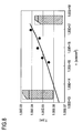
- samples A to E having a thermally oxidized layer (cluster protection layer) with different film thicknesses within the range of 50 nm to 2 ⁇ m were fabricated. After GCIB irradiation as will be described later in each example, the thermally oxidized film used as the cluster protection layer was ashed and removed by an ashing apparatus.
- the thermally oxidized film was considered to be functioning as a cluster protection layer (that is, corners of the silicon pattern will not be deformed). If the relationship was below the curve, the film was considered not to be functioning as a cluster protection layer.
- the mean surface roughness of the side walls of the line was measured by an atomic force microscope (AFM) before and after the GCIB irradiation.
- AFM atomic force microscope
- the mean surface roughness of the side wall of the line was measured, the samples were cut to expose the line side wall.
- the mean surface roughness (Ra) of the line side wall before the GCIB irradiation was 3.8 nm.
- the mean line width was 1.00 ⁇ m
- the mean surface roughness (Ra) of the line side wall was 0.52 nm.
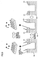
- An SF 6 gas cluster ion beam was alternately emitted to opposite side walls of a line at an angle ⁇ of 7°.
- the example is illustrated in Fig. 9 .
- the dose was 1.0*10 14 ions/cm 2 for each side, and the opposite sides were irradiated alternately.
- the pattern width was 1.00 ⁇ m, and the roughness (Ra) of the line side wall was 0.49 nm.
- the silicon line had an oblique angle ⁇ of 0 degrees, indicating that the corners were not deformed.
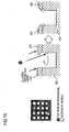
- a pattern structure formed by an array of cylindrical recesses in silicon (diameter of 1 ⁇ m, square array with a pitch of 1 ⁇ m) was fabricated by the same method as for the line-and-space patterns of the examples described above.
- the silicon substrate was rotated in the plane while the side wall of the cylindrical recess was irradiated with the GCIB at an angle ⁇ of 7°.
- This example is illustrated in Fig. 10 .
- the left diagram of Fig. 10 is a plan view of the pattern of the array of cylinderical recesses, and the arrow represents the in-plane rotation of the silicon substrate.
- the right diagram of Fig. 10 is a cross sectional view of the cylindrical recess.
- the dose was 3.0*10 15 ions/cm 2 .
- the thickness T of the thermally oxidized film was 0.6 ⁇ m.
- the pattern width was 1.00 ⁇ m, and the mean surface roughness (Ra) of the side wall of the cylindrical recess was 0.49 nm.
- the angle ⁇ of the upper part of the silicon protrusion was 0 degrees, which was the same as the designed value.
- the first, second, and third examples show that the line width can be adjusted without deforming the corners of the upper part of the line-and-space pattern structure in the solid state, by adjusting the line width by using a thermally oxidized film having a thickness satisfying Equation (7) as a cluster protection layer and then removing the thermally oxidized film.
- the accelerating voltage was 30 kV. As the accelerating voltage increases, the etching amount increases, reducing the smoothing time. On the other hand, increased accelerating voltage could degrade the surface roughness. Therefore, the accelerating voltage should be determined in accordance with the requirements of solid surface processing, such as time and material. Neither the parameters nor the apparatus conditions, such as gas type, irradiation conditions, and cluster size, is limited and the parameters and the apparatus conditions can be changed as necessary.
- the present invention can be applied to the fabrication of high-precision three-dimensional structures such as high-performance semiconductor devices or optical devices and dies for fabricating those devices.
- a gas cluster ion beam is emitted onto a solid surface having a relief structure with a cluster protection layer formed to cover it, so that corner portions of the relief structure can be protected from deformation.
Landscapes
- Drying Of Semiconductors (AREA)
- Welding Or Cutting Using Electron Beams (AREA)
Applications Claiming Priority (2)
| Application Number | Priority Date | Filing Date | Title |
|---|---|---|---|
| JP2006293687 | 2006-10-30 | ||
| PCT/JP2007/071459 WO2008054013A1 (fr) | 2006-10-30 | 2007-10-30 | Procédé de façonnage d'une surface solide faisant intervenir un faisceau ionique à agrégats gazeux |
Publications (2)
| Publication Number | Publication Date |
|---|---|
| EP2079103A1 true EP2079103A1 (de) | 2009-07-15 |
| EP2079103A4 EP2079103A4 (de) | 2010-05-26 |
Family
ID=39344348
Family Applications (1)
| Application Number | Title | Priority Date | Filing Date |
|---|---|---|---|
| EP07831192A Withdrawn EP2079103A4 (de) | 2006-10-30 | 2007-10-30 | Verfahren zur bearbeitung einer festen oberfläche mit einem gascluster-ionenstrahl |
Country Status (6)
| Country | Link |
|---|---|
| US (1) | US8268183B2 (de) |
| EP (1) | EP2079103A4 (de) |
| JP (2) | JP5160437B2 (de) |
| KR (1) | KR101055633B1 (de) |
| CN (1) | CN101563759B (de) |
| WO (1) | WO2008054013A1 (de) |
Cited By (1)
| Publication number | Priority date | Publication date | Assignee | Title |
|---|---|---|---|---|
| WO2012044677A1 (en) * | 2010-10-01 | 2012-04-05 | Varian Semiconductor Equipment Assoclates, Inc. | Method and system for modifying patterned photoresist using multi-step ion implantion |
Families Citing this family (23)
| Publication number | Priority date | Publication date | Assignee | Title |
|---|---|---|---|---|
| US6869812B1 (en) | 2003-05-13 | 2005-03-22 | Heng Liu | High power AllnGaN based multi-chip light emitting diode |
| JP5031066B2 (ja) * | 2010-05-26 | 2012-09-19 | 兵庫県 | クラスタービーム発生装置、基板処理装置、クラスタービーム発生方法及び基板処理方法 |
| US8354655B2 (en) * | 2011-05-03 | 2013-01-15 | Varian Semiconductor Equipment Associates, Inc. | Method and system for controlling critical dimension and roughness in resist features |
| JP5720473B2 (ja) * | 2011-07-28 | 2015-05-20 | 株式会社デンソー | 半導体装置の製造方法 |
| US8512586B2 (en) | 2011-09-01 | 2013-08-20 | Tel Epion Inc. | Gas cluster ion beam etching process for achieving target etch process metrics for multiple materials |
| US8513138B2 (en) | 2011-09-01 | 2013-08-20 | Tel Epion Inc. | Gas cluster ion beam etching process for Si-containing and Ge-containing materials |
| US8557710B2 (en) | 2011-09-01 | 2013-10-15 | Tel Epion Inc. | Gas cluster ion beam etching process for metal-containing materials |
| US8722542B2 (en) | 2012-06-08 | 2014-05-13 | Tel Epion Inc. | Gas cluster ion beam process for opening conformal layer in a high aspect ratio contact via |
| US8728947B2 (en) | 2012-06-08 | 2014-05-20 | Tel Epion Inc. | Gas cluster ion beam process for opening conformal layer in a high aspect ratio contact via |
| JP5925642B2 (ja) * | 2012-08-31 | 2016-05-25 | 日本航空電子工業株式会社 | 無機固体材料および刃物工具 |
| JP5683640B2 (ja) * | 2013-05-20 | 2015-03-11 | 日本航空電子工業株式会社 | 刃物工具 |
| US9209033B2 (en) | 2013-08-21 | 2015-12-08 | Tel Epion Inc. | GCIB etching method for adjusting fin height of finFET devices |
| JP6421759B2 (ja) * | 2013-10-24 | 2018-11-14 | コニカミノルタ株式会社 | 精密研磨装置及び方法 |
| KR102347960B1 (ko) | 2015-02-03 | 2022-01-05 | 삼성전자주식회사 | 도전체 및 그 제조 방법 |
| CN108232007A (zh) * | 2016-12-21 | 2018-06-29 | 上海磁宇信息科技有限公司 | 一种气体团簇离子束修剪被刻蚀后的磁性隧道结的方法 |
| US10649141B1 (en) * | 2018-04-23 | 2020-05-12 | Facebook Technologies, Llc | Gratings with variable etch heights for waveguide displays |
| US10732351B2 (en) | 2018-04-23 | 2020-08-04 | Facebook Technologies, Llc | Gratings with variable depths formed using planarization for waveguide displays |
| US11067726B2 (en) | 2018-04-23 | 2021-07-20 | Facebook Technologies, Llc | Gratings with variable depths for waveguide displays |
| US20200135898A1 (en) * | 2018-10-30 | 2020-04-30 | International Business Machines Corporation | Hard mask replenishment for etching processes |
| US11195703B2 (en) | 2018-12-07 | 2021-12-07 | Applied Materials, Inc. | Apparatus and techniques for angled etching using multielectrode extraction source |
| US11715621B2 (en) | 2018-12-17 | 2023-08-01 | Applied Materials, Inc. | Scanned angled etching apparatus and techniques providing separate co-linear radicals and ions |
| JP7382809B2 (ja) * | 2019-12-02 | 2023-11-17 | キヤノントッキ株式会社 | 成膜方法及び成膜装置 |
| CN120092314A (zh) * | 2022-11-02 | 2025-06-03 | Agc株式会社 | 制造具有凹部结构的部件的方法和具有凹部结构的部件 |
Family Cites Families (6)
| Publication number | Priority date | Publication date | Assignee | Title |
|---|---|---|---|---|
| JPH05102083A (ja) | 1991-10-08 | 1993-04-23 | Toshiba Corp | ドライエツチング方法及びそのための装置 |
| JPH06291095A (ja) | 1993-03-31 | 1994-10-18 | Hitachi Ltd | パターン形成方法 |
| TWI295303B (en) * | 2003-08-21 | 2008-04-01 | Toyo Boseki | Optical-use adhesive polyester film and optical-use laminatede film |
| JP3994111B2 (ja) | 2003-09-30 | 2007-10-17 | 日本航空電子工業株式会社 | 固体表面の平坦化方法及びその装置 |
| JP4312574B2 (ja) * | 2003-10-31 | 2009-08-12 | 独立行政法人産業技術総合研究所 | イオンビーム加工装置およびイオンビーム加工方法 |
| JP3816484B2 (ja) | 2003-12-15 | 2006-08-30 | 日本航空電子工業株式会社 | ドライエッチング方法 |
-
2007
- 2007-10-30 EP EP07831192A patent/EP2079103A4/de not_active Withdrawn
- 2007-10-30 US US12/312,266 patent/US8268183B2/en active Active
- 2007-10-30 CN CN2007800406780A patent/CN101563759B/zh active Active
- 2007-10-30 WO PCT/JP2007/071459 patent/WO2008054013A1/ja not_active Ceased
- 2007-10-30 KR KR1020097008402A patent/KR101055633B1/ko active Active
- 2007-10-30 JP JP2008542206A patent/JP5160437B2/ja active Active
-
2012
- 2012-02-02 JP JP2012020899A patent/JP5499062B2/ja active Active
Cited By (1)
| Publication number | Priority date | Publication date | Assignee | Title |
|---|---|---|---|---|
| WO2012044677A1 (en) * | 2010-10-01 | 2012-04-05 | Varian Semiconductor Equipment Assoclates, Inc. | Method and system for modifying patterned photoresist using multi-step ion implantion |
Also Published As
| Publication number | Publication date |
|---|---|
| JP5499062B2 (ja) | 2014-05-21 |
| CN101563759A (zh) | 2009-10-21 |
| JPWO2008054013A1 (ja) | 2010-02-25 |
| JP5160437B2 (ja) | 2013-03-13 |
| US20090305507A1 (en) | 2009-12-10 |
| EP2079103A4 (de) | 2010-05-26 |
| KR20090074217A (ko) | 2009-07-06 |
| WO2008054013A1 (fr) | 2008-05-08 |
| KR101055633B1 (ko) | 2011-08-09 |
| JP2012104858A (ja) | 2012-05-31 |
| CN101563759B (zh) | 2011-08-03 |
| US8268183B2 (en) | 2012-09-18 |
Similar Documents
| Publication | Publication Date | Title |
|---|---|---|
| US8268183B2 (en) | Method of processing solid surface with gas cluster ion beam | |
| EP2079102B1 (de) | Verfahren zur verflachung einer festen oberfläche mit einem gascluster-ionenstrahl | |
| US8481981B2 (en) | Method of smoothing solid surface with gas cluster ion beam and solid surface smoothing apparatus | |
| Lu et al. | Patterning of highly oriented pyrolytic graphite by oxygen plasma etching | |
| TWI532103B (zh) | 製造鰭狀場效電晶體的方法和製造裝置的方法 | |
| TW202036721A (zh) | 用來蝕刻含碳特徵之方法 | |
| JP5264237B2 (ja) | ナノ構造体およびナノ構造体の製造方法 | |
| JP2003158099A5 (de) | ||
| KR20210061445A (ko) | 깊이 변조된 각진 격자들을 갖는 광학적 컴포넌트 및 형성 방법 | |
| CN101554991B (zh) | 一种多样性纳米结构的加工方法 | |
| JP5782460B2 (ja) | 材料除去及びパターン転写の方法及びシステム | |
| US20020139770A1 (en) | Methods for fabricating segmented reticle blanks having uniformly machined grillage, and reticle blanks and reticles formed thereby | |
| Li et al. | Bulk Silicon Microfabrication Technology | |
| Cui | Nanoscale Pattern Transfer | |
| Hilleringmann | Etching Technology | |
| JP4025886B2 (ja) | 結晶TiO2の微細加工方法及び微細加工された結晶TiO2 | |
| JP2001201627A (ja) | 回折素子の製造方法 | |
| JP2006239787A (ja) | 微細構造作製方法及び装置 | |
| Sheu et al. | Silicon Nanomachining by Scanning Probe Lithography and Anisotropic Wet Etching | |
| Sheua et al. | SILICON NANOMACillNING PROBE LITHOGRAPHY AND WETETCIDNG | |
| JPS63318739A (ja) | 微細パタ−ンの形成方法 | |
| JPH02192716A (ja) | 電子ビーム描画方法 |
Legal Events
| Date | Code | Title | Description |
|---|---|---|---|
| PUAI | Public reference made under article 153(3) epc to a published international application that has entered the european phase |
Free format text: ORIGINAL CODE: 0009012 |
|
| 17P | Request for examination filed |
Effective date: 20090423 |
|
| AK | Designated contracting states |
Kind code of ref document: A1 Designated state(s): AT BE BG CH CY CZ DE DK EE ES FI FR GB GR HU IE IS IT LI LT LU LV MC MT NL PL PT RO SE SI SK TR |
|
| A4 | Supplementary search report drawn up and despatched |
Effective date: 20100428 |
|
| RIC1 | Information provided on ipc code assigned before grant |
Ipc: H01L 21/308 20060101ALI20100422BHEP Ipc: H01L 21/033 20060101ALI20100422BHEP Ipc: H01L 21/302 20060101AFI20080612BHEP |
|
| STAA | Information on the status of an ep patent application or granted ep patent |
Free format text: STATUS: THE APPLICATION IS DEEMED TO BE WITHDRAWN |
|
| 18D | Application deemed to be withdrawn |
Effective date: 20100116 |