EP2079290A2 - Topologie de circuit passif multicouche - Google Patents
Topologie de circuit passif multicouche Download PDFInfo
- Publication number
- EP2079290A2 EP2079290A2 EP09150384A EP09150384A EP2079290A2 EP 2079290 A2 EP2079290 A2 EP 2079290A2 EP 09150384 A EP09150384 A EP 09150384A EP 09150384 A EP09150384 A EP 09150384A EP 2079290 A2 EP2079290 A2 EP 2079290A2
- Authority
- EP
- European Patent Office
- Prior art keywords
- multilayer
- layer
- inductor
- circuit
- conductive traces
- Prior art date
- Legal status (The legal status is an assumption and is not a legal conclusion. Google has not performed a legal analysis and makes no representation as to the accuracy of the status listed.)
- Granted
Links
Images


Classifications
-
- H—ELECTRICITY
- H05—ELECTRIC TECHNIQUES NOT OTHERWISE PROVIDED FOR
- H05K—PRINTED CIRCUITS; CASINGS OR CONSTRUCTIONAL DETAILS OF ELECTRIC APPARATUS; MANUFACTURE OF ASSEMBLAGES OF ELECTRICAL COMPONENTS
- H05K1/00—Printed circuits
- H05K1/16—Printed circuits incorporating printed electric components, e.g. printed resistors, capacitors or inductors
- H05K1/165—Printed circuits incorporating printed electric components, e.g. printed resistors, capacitors or inductors incorporating printed inductors
-
- H—ELECTRICITY
- H01—ELECTRIC ELEMENTS
- H01F—MAGNETS; INDUCTANCES; TRANSFORMERS; SELECTION OF MATERIALS FOR THEIR MAGNETIC PROPERTIES
- H01F17/00—Fixed inductances of the signal type
- H01F17/0006—Printed inductances
- H01F17/0013—Printed inductances with stacked layers
-
- H—ELECTRICITY
- H01—ELECTRIC ELEMENTS
- H01F—MAGNETS; INDUCTANCES; TRANSFORMERS; SELECTION OF MATERIALS FOR THEIR MAGNETIC PROPERTIES
- H01F17/00—Fixed inductances of the signal type
- H01F17/0006—Printed inductances
- H01F17/0033—Printed inductances with the coil helically wound around a magnetic core
-
- H—ELECTRICITY
- H03—ELECTRONIC CIRCUITRY
- H03H—IMPEDANCE NETWORKS, e.g. RESONANT CIRCUITS; RESONATORS
- H03H1/00—Constructional details of impedance networks whose electrical mode of operation is not specified or applicable to more than one type of network
- H03H2001/0021—Constructional details
- H03H2001/0085—Multilayer, e.g. LTCC, HTCC, green sheets
-
- H—ELECTRICITY
- H03—ELECTRONIC CIRCUITRY
- H03H—IMPEDANCE NETWORKS, e.g. RESONANT CIRCUITS; RESONATORS
- H03H7/00—Multiple-port networks comprising only passive electrical elements as network components
- H03H7/01—Frequency selective two-port networks
- H03H7/0115—Frequency selective two-port networks comprising only inductors and capacitors
-
- H—ELECTRICITY
- H05—ELECTRIC TECHNIQUES NOT OTHERWISE PROVIDED FOR
- H05K—PRINTED CIRCUITS; CASINGS OR CONSTRUCTIONAL DETAILS OF ELECTRIC APPARATUS; MANUFACTURE OF ASSEMBLAGES OF ELECTRICAL COMPONENTS
- H05K1/00—Printed circuits
- H05K1/16—Printed circuits incorporating printed electric components, e.g. printed resistors, capacitors or inductors
- H05K1/162—Printed circuits incorporating printed electric components, e.g. printed resistors, capacitors or inductors incorporating printed capacitors
-
- H—ELECTRICITY
- H05—ELECTRIC TECHNIQUES NOT OTHERWISE PROVIDED FOR
- H05K—PRINTED CIRCUITS; CASINGS OR CONSTRUCTIONAL DETAILS OF ELECTRIC APPARATUS; MANUFACTURE OF ASSEMBLAGES OF ELECTRICAL COMPONENTS
- H05K2201/00—Indexing scheme relating to printed circuits covered by H05K1/00
- H05K2201/09—Shape and layout
- H05K2201/09209—Shape and layout details of conductors
- H05K2201/09654—Shape and layout details of conductors covering at least two types of conductors provided for in H05K2201/09218 - H05K2201/095
- H05K2201/09672—Superposed layout, i.e. in different planes
-
- H—ELECTRICITY
- H05—ELECTRIC TECHNIQUES NOT OTHERWISE PROVIDED FOR
- H05K—PRINTED CIRCUITS; CASINGS OR CONSTRUCTIONAL DETAILS OF ELECTRIC APPARATUS; MANUFACTURE OF ASSEMBLAGES OF ELECTRICAL COMPONENTS
- H05K2201/00—Indexing scheme relating to printed circuits covered by H05K1/00
- H05K2201/09—Shape and layout
- H05K2201/09209—Shape and layout details of conductors
- H05K2201/09654—Shape and layout details of conductors covering at least two types of conductors provided for in H05K2201/09218 - H05K2201/095
- H05K2201/097—Alternating conductors, e.g. alternating different shaped pads, twisted pairs; Alternating components
-
- H—ELECTRICITY
- H05—ELECTRIC TECHNIQUES NOT OTHERWISE PROVIDED FOR
- H05K—PRINTED CIRCUITS; CASINGS OR CONSTRUCTIONAL DETAILS OF ELECTRIC APPARATUS; MANUFACTURE OF ASSEMBLAGES OF ELECTRICAL COMPONENTS
- H05K3/00—Apparatus or processes for manufacturing printed circuits
- H05K3/40—Forming printed elements for providing electric connections to or between printed circuits
- H05K3/42—Plated through-holes or plated via connections
- H05K3/429—Plated through-holes specially for multilayer circuits, e.g. having connections to inner circuit layers
Definitions
- the present invention relates generally to communications, and more particularly to a multilayer passive circuit topology.
- RF and IF filters are typically used in RF Communications Transceivers (Transmitters and Receivers) for pre- or post-selection of desired signals.
- Filters are typically sub-octave and enhance receiver (RX) selectivity by rejecting unwanted signals at image frequencies and other points of spurious sensitivity.
- RX enhance receiver
- filters reject unwanted spurious and harmonics prior to final RF power amplification.
- Filters are also used at intermediate frequencies in both up/down conversion architecture to reject unwanted signals, as described above.
- filter response is required to roll-off rapidly outside the band of interest, necessitating a high order filter.
- in-band loss must be minimized through the filter to minimize signal degradation.
- precision less than 2% tolerance
- high-Q Quality factor
- capacitor lumped element implementations Such elements typically have Q's greater than 100 and are typically required for narrow band or high rejection stopband/selectivity performance.
- high performance lumped filters require significant touch labor for assembly and tuning.
- Typical integrated microwave assemblies use LC (inductor-capacitor) filters utilizing air core solenoid wire inductors (air or wrapped coil-forms) and parallel plate capacitors that are hand trimmed and tuned, as surface mount components usually do not have the required precision, nor the necessary Q. The latter is especially pertinent to smaller solenoidal SMT inductors, usually attaining precision between 2% to 5% and Q's less than 100 for optimal small sizes.
- Other implementations of solenoidal inductors are referenced in United States Patent no. 7,088,215 , entitled, "Embedded Duo Planar Printed Inductor", the entire content of which is hereby incorporated herein.
- hand tuned filters increases exponentially with the order of the filter.
- hand tuned lumped filters are packaged to ensure electrical performance and isolation.
- Highest Q inductors are typically constructed with air cores and require large volumes. Consequently inductor diameters for lower frequency filter applications (below 1 GHz) are large and result in package heights to greater than 0.25 inches. This height is unacceptable for many compact filter requirements.
- tight packing densities induce interaction with other inductor elements, reducing performance and increasing tuning complexities. Additional walls are thus typically added for effective isolation and/or rejection, increasing complexity and adding cost and size.
- a multilayer circuit comprises a multilayer inductor comprising a first set of parallel conductive traces formed on a first layer, a second set of parallel conductive traces formed on a second layer spaced apart from the first layer; and a plurality of vias that connect respective parallel conductive traces from the first and second layers to form inductor windings.
- the multilayer circuit further comprises a multilayer capacitor connected to an end of the inductor by a coupling via, the capacitor comprising a first conductive plate and a second conductive plate being spaced apart from one another and being formed on different layers.
- the multilayer circuit comprises a plurality of multilayer inductors, each multilayer inductor being formed from a first set of parallel conductive traces and a second set of parallel conductive traces formed on different spaced apart layers and a plurality of vias that connect respective parallel conductive traces from the different layers to form inductor windings.
- the multilayer circuit further comprises a plurality of multilayer capacitors, each multilayer capacitor being formed from a first conductive plate and a second conductive plate formed on different layers wherein the plurality of multilayer inductors and the plurality multilayer capacitors are arranged in a circuit.
- the multilayer circuit has a plurality of tuning capacitors coupled on opposing ends of each of the plurality of multilayer inductors and/or a plurality of sets of a plurality of spaced apart parallel vias arranged to form faraday cages to surround and isolate each of the multilayer inductors and associated tuning capacitors.
- a method of fabricating a multilayer circuit comprises etching a first set of parallel conductive traces on a first layer, etching a second set of parallel conductive traces on a second layer spaced apart from the first layer and forming a plurality of vias that connect respective parallel conductive traces from the first and second layers to form a multilayer inductor.
- the method further comprises etching a first conductive plate on a third layer; etching a second conductive plate on a fourth layer being spaced apart from third layer to form a multilayer capacitor and forming a coupling via that connects the multilayer inductor to the multilayer capacitor.
- the etching a first set of parallel conductive traces on a first layer, the etching a second set of parallel conductive traces on a second layer spaced apart from the first layer and the forming a plurality of vias that connect respective parallel conductive traces from the first and second layers to form a multilayer inductor comprises etching a plurality of sets of a first set of parallel conductive traces on the first layer, etching a plurality of sets of a second set of parallel conductive traces on the second layer spaced apart from the first layer and forming a plurality of sets of the plurality of vias that connect respective parallel conductive traces from the first and second layers to form a plurality of multilayer inductors.
- the etching a first conductive plate on a third layer, the etching a second conductive plate on a fourth layer being spaced apart from third layer to form a multilayer capacitor and the forming a coupling via that connects the multilayer inductor to the multilayer capacitor comprises etching a plurality of sets of a first conductive plate on a third layer comprises etching a plurality of sets of a second conductive plate on a fourth layer being spaced apart from third layer to form a plurality of multilayer capacitors and forming a plurality of sets of a coupling via that connects the multilayer inductors to the multilayer capacitors.
- the plurality of multilayer inductors and plurality of multilayer capacitors are arranged as a plurality of inductor-capacitor circuits interconnected with one another to form a multipole filter. Still further optionally the method further comprises coupling a plurality of tuning capacitors on opposing ends of each of the plurality of multilayer inductors and forming a plurality of sets of a plurality of space apart parallel vias arranged to form faraday cages to surround and isolate each of the multilayer inductor and associated tuning capacitors.
- FIG. 1 illustrates a cross-section of a multi-layer passive circuit in accordance with an aspect of the present invention.
- FIG. 2 illustrates a perspective view of a multilayer inductor in accordance with an aspect of the invention.
- FIG. 3 illustrates a perspective view of a multilayer capacitor in accordance with an aspect of the invention.
- FIG. 4 illustrates a perspective view of a multi-layer inductor-capacitor (LC) circuit in accordance with an aspect of the present invention.
- LC inductor-capacitor
- FIG. 5 illustrates a schematic drawing of a sixth order tubular filter topology in accordance with an aspect of the present invention.
- FIG. 6 illustrates a top view of an exemplary integrated filter employing the sixth order tubular filter topology of FIG. 5 in accordance with an aspect of the present invention.
- FIG. 7 illustrates a methodology for fabricating a multilayer circuit in accordance with an aspect of the present invention.
- the present invention relates to a multilayer passive circuit topology supporting any applications requiring precision inductors and capacitors in a low cost material.
- the multilayer passive circuit topology provides inductor-capacitor (LC) circuits formed from multilayer inductors and multilayer capacitors that can be configured as filters, matching structures, resonators, oscillators or a variety of other LC circuit types.
- LC inductor-capacitor
- the result is a low cost, highly selective and repeatable multilayer passive structure that can be integrated into a multilayer structure, such as a printed wiring board (PWB) or can be separately surface mounted as a sub-assembly in a manner that minimizes component height, supporting dense electronics packaging.
- the multilayer passive circuit topology allows for production of sub 2% inductors due to reduced parasitics, reduced inductor capacitance and the ability to provide very tight tolerances.
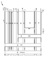
- FIG. 1 illustrates a cross-section of a multi-layer passive circuit 10 in accordance with an aspect of the present invention.
- the multi-layer passive circuit 10 is a single inductor-capacitor (LC) circuit that can be employed as, for example, a filter and yields a highly producible passive circuit using multilayer embedded passive components.
- the present example is illustrated with respect to a PWB but could be formed on a number of different multilayer structures, such as a low temperature co-fired ceramic (LTCC) structure, a multilayer semiconductor structure, a monolithic microwave integrated circuit (MMIC), liquid crystal polymer (LCP) structures or another type of multilayer circuit structure.
- LTCC low temperature co-fired ceramic
- MMIC monolithic microwave integrated circuit
- LCP liquid crystal polymer
- Other suitable technologies would include RFIC processes including but not limited to SiGe, GaAs, GaN, etc.
- the multi-layer passive circuit includes a top microstrip layer 12 that forms a poured ground layer disposed above a first dielectric layer 14 that is disposed above a second dielectric layer 16.
- a multilayer capacitor is formed below the second dielectric layer 16.
- the multilayer capacitor is formed by a first metal plate layer 18, a third dielectric layer 20 disposed below the first metal plate layer 18, and a second metal plate layer 22 is disposed below the third dielectric layer 20.
- a parallel plate pair C1, C2 on the first metal plate layer 18 and second metal plate layer 22 form the multilayer capacitor.
- a fourth dielectric layer 24, a fifth dielectric layer 26 and a sixth dielectric layer 28 are disposed beneath the multilayer capacitor.
- a metal ground layer 30 (gnd2) is disposed beneath the sixth dielectric layer 28 followed by a seventh dielectric layer 32 and an eight dielectric layer 34.
- a multilayer inductor is disposed beneath the eighth dielectric layer 34.
- the multilayer inductor is formed by a first conductive trace layer 36, a ninth dielectric layer 38 disposed below the first conductive trace layer 36, and a second conductive trace layer 40 disposed below the ninth dielectric layer 38.
- the multilayer inductor is comprised of a first set of parallel conductive traces L2 formed on the first conductive trace layer 36, a second set of parallel conductive traces L1 formed on the second conductive trace layer 40 and a plurality of buried vias 48 coupling respective parallel conductive traces from the first and second conductive trace layers 36 and 40.
- a tenth dielectric layer 42 and an eleventh dielectric layer 44 are disposed beneath the multilayer inductor and a ground layer 46 (gnd1) is disposed beneath the eleventh dielectric layer 44.
- the first, third, fifth, seventh, ninth and eleventh dielectric layers can be formed of a first dielectric material such as Rogers R3003.
- the second, fourth, sixth, eight and tenth dielectric layers can be formed of a second dielectric material, such as GETEK.
- Through vias (VIA3) are used to connect between the microstrip layer and the buried multilayer capacitor and multilayer inductor. Ground is implemented with through vias (VIA3 (gnd)) and the blind via (VIA2).
- This structure of FIG. 1 can comprise a standalone surface mount PWB "brick" or be implemented in a greater PWB structure.
- FIG. 2 illustrates a perspective view of a multilayer inductor 60 in accordance with an aspect of the invention.
- the multilayer inductor 60 may be an exemplary embedded rectangular inductor that can be built using the first and second conduct trace layers 36 and 40 and the plurality of buried vias 48 as shown in FIG. 1 .
- a first set of parallel horizontal conducive traces 62 (L2) are etched on the first conductive trace layer 36 and a second set of parallel horizontal conducive traces 64 (L1) are etched on the second conductive trace layer 40 with embedded vias 48 employed to connect respective conductive traces on the first and second conductive trace layers 36 and 40 to form rectangular solenoid windings.
- Two through-vias 52 are employed as input/outports to bring the signal in and out of the inductor.
- Two ground layers 30 and 46 and a set of ground vias 50 (not shown) around the periphery of the inductor are used to contain the electric field.
- the following parameters affect the performance of the inductor: number of turns, trace width and spacing, core material (thickness, dielectric constant, loss tangent), via size, and metallization.
- EM simulation tools can be used to optimize the design, typically to achieve a producible, high Q inductor of the desired inductance value. Repeatable (within production lots) inductors with very high Qs, in the range of 120-150, are achievable.
- FIG. 3 illustrates a perspective view of a multilayer capacitor 70 in accordance with an aspect of the invention.
- the multilayer capacitor 70 may be an exemplary embedded capacitor that can be built using the first and second metal plate layers 18 and 22 as shown in FIG. 1 .
- a first metal plate C1 of a desired area is etched on the second metal plate layer 22 and a second metal plate C2 of a similar area is etched on the first metal plate layer 18 in a parallel relationship to one another forming a multilayer capacitor.
- core material thickness, dielectric constant and loss tangent
- metal plate dimensions area and etch variation.
- Two through-vias 52 are employed as input/output to bring the signal in and out of the capacitor and couple the multilayer capacitor to the multilayer inductor.
- Two ground layers 12 and 30 isolate the capacitor 70 from the inductor 60.
- FIG. 4 illustrates a multi-layer LC circuit 80 that includes multiple multilayer inductors 86 and multiple multilayer capacitors 88 coupled in a LC circuit series configuration.
- a first through via 82 and a second through via 84 are provided as input/output ports of the multilayer passive circuit 80.
- Each of a set of multilayer inductors 86 are serially coupled to respective ones of each of a set of multilayer capacitors 88 via coupling vias 92 to form respective multilayer LC circuits.
- the multilayer LC circuits are coupled to one another via connecting vias 90 to form the multiple multilayer LC circuits 80 coupled in a series configuration.
- the multilayer LC circuit 80 can be configured as a multiple pole filter. It is to be appreciated that the passive circuits could include resistor elements 94, for example, be employing a resistive material to form RLC, RL, or RC circuits. It is also to be appreciated that although the inductors and capacitors are illustrated on different multiple layers, the capacitors and inductors could share layers. Furthermore, although the inductors are illustrated as disposed in layers beneath the capacitors, it is to be appreciated that the inductors can reside in layers above the capacitors without effecting the operation of the multi-layer passive circuit 80.
- the multilayer passive components can be used to construct filters with broad ranges of bandwidths and filter orders. Since embedded multilayer passive components can be employed to implement both series and shunt components, therefore the employment of multilayer passive components can be employed to be used for substantially any filter topology. It is also to be appreciated that mixed or "hybrid" combinations of distributed structures (transmission lines, radial elements, etc) can provide additional filtering capabilities.
- FIG. 5 illustrates a schematic drawing of a sixth order tubular filter topology 100 in accordance with an aspect of the present invention.
- the sixth order tubular filter topology 100 include six multilayer embedded series coupled LC circuits connected between an input port and an output port.
- a surface mount shunt chip capacitor couples each intermediate node to ground.
- the surface mount shunt chip capacitors are employed to tune the filter. In this design all the series components were implemented using embedded passives and high precision discrete shunt capacitors were used to tune the filter.
- Each multilayer embedded inductor is electrically isolated from one another employing a faraday cage 102 formed of a plurality of spaced apart parallel vias.
- FIG. 6 illustrates a top view of an exemplary integrated filter 110 employing the sixth order tubular filter topology of FIG. 5 in accordance with an aspect of the present invention.
- the shunt capacitors are left as discrete high precision parts due to size considerations but primarily to give the filter tunability. Variation in the accuracy of the embedded passives can be compensated by adjusting the shunt capacitor values. Variation between production PWB lots will be minimal, and once a filter is aligned by varying the discrete shunt capacitors, the same changes can be applied to rest of the boards from that lot without having to retune each one individually.
- Other implementations could use tunable varactor diodes, micromachined electro-mechanical (MEMs) switches, or tunable dielectric materials to effect filter tuning.
- MEMs micromachined electro-mechanical
- multilayer embedded passive circuits inductors and capacitors
- inductors and capacitors rather than hand-tuned inductors and capacitors, can greatly reduce filter production time, cost, weight and volume.
- the result is a low cost, highly selective and repeatable multilayer embedded passive filter structure that can be integrated into a printed wiring board or separately surface mounted as a sub-assembly in a manner that minimizes component height, supporting dense electronics packaging.
- FIG. 7 illustrates a methodology for fabricating a multilayer circuit in accordance with an aspect of the present invention.
- a first set of parallel conductive traces are etched on a first layer.
- a second set of parallel conductive traces are etched on a second layer spaced apart from the first layer.
- a plurality of vias are formed that connect respective parallel conductive traces from the first and second layers to form a multilayer inductor.
- the methodology then proceeds to 230.
- a first conductive plate is formed on a third layer.
- a second conductive plate is formed on a fourth layer spaced apart from the third layer to form a multilayer capacitor.
- a coupling via is formed that connects the multilayer inductor to the multilayer capacitor. It is to be appreciated that the methodology is not limited to the fabrication of a single LC circuit, but that a plurality of inductors and capacitors can be formed and arranged to build a variety of different circuit configurations (e.g., filters, matching structures, resonators, oscillators or a variety of other LC circuit types).
Landscapes
- Engineering & Computer Science (AREA)
- Microelectronics & Electronic Packaging (AREA)
- Coils Or Transformers For Communication (AREA)
- Filters And Equalizers (AREA)
- Parts Printed On Printed Circuit Boards (AREA)
Applications Claiming Priority (1)
| Application Number | Priority Date | Filing Date | Title |
|---|---|---|---|
| US12/013,170 US7724117B2 (en) | 2008-01-11 | 2008-01-11 | Multilayer passive circuit topology |
Publications (3)
| Publication Number | Publication Date |
|---|---|
| EP2079290A2 true EP2079290A2 (fr) | 2009-07-15 |
| EP2079290A3 EP2079290A3 (fr) | 2010-03-17 |
| EP2079290B1 EP2079290B1 (fr) | 2016-08-03 |
Family
ID=40352626
Family Applications (1)
| Application Number | Title | Priority Date | Filing Date |
|---|---|---|---|
| EP09150384.7A Active EP2079290B1 (fr) | 2008-01-11 | 2009-01-12 | Topologie de circuit passif multicouche |
Country Status (2)
| Country | Link |
|---|---|
| US (1) | US7724117B2 (fr) |
| EP (1) | EP2079290B1 (fr) |
Cited By (5)
| Publication number | Priority date | Publication date | Assignee | Title |
|---|---|---|---|---|
| WO2011045264A3 (fr) * | 2009-10-14 | 2011-06-23 | Robert Bosch Gmbh | Dispositif de protection contre les interférences électromagnétiques |
| WO2017200693A1 (fr) * | 2016-05-20 | 2017-11-23 | Qualcomm Incorporated | Appareil avec bobine d'induction 3d intégrée dans un substrat |
| WO2017200703A1 (fr) * | 2016-05-20 | 2017-11-23 | Qualcomm Incorporated | Composants passifs mis en œuvre sur une pluralité d'isolants empilés |
| WO2020027975A1 (fr) * | 2018-08-01 | 2020-02-06 | Qualcomm Incorporated | Structure passive tridimensionnelle de haute qualité ayant une technologie de colonne conductrice |
| CN115499035A (zh) * | 2022-11-15 | 2022-12-20 | 安徽大学 | 一种基于ltcc的射频模组及基站设备 |
Families Citing this family (18)
| Publication number | Priority date | Publication date | Assignee | Title |
|---|---|---|---|---|
| KR101055483B1 (ko) * | 2009-04-07 | 2011-08-08 | 포항공과대학교 산학협력단 | 전자기 밴드갭 구조물 및 이를 포함하는 인쇄회로기판 |
| KR101055457B1 (ko) * | 2009-04-07 | 2011-08-08 | 포항공과대학교 산학협력단 | 전자기 밴드갭 구조물 및 이를 포함하는 인쇄회로기판 |
| FR2961345A1 (fr) * | 2010-06-10 | 2011-12-16 | St Microelectronics Tours Sas | Circuit integre passif |
| KR20130051614A (ko) * | 2011-11-10 | 2013-05-21 | 삼성전기주식회사 | 적층 세라믹 전자 부품 및 그 제조 방법 |
| US8643184B1 (en) * | 2012-10-31 | 2014-02-04 | Intel Corporation | Crosstalk polarity reversal and cancellation through substrate material tuning |
| US20140240071A1 (en) * | 2013-02-26 | 2014-08-28 | Entropic Communications, Inc. | 3d printed inductor |
| US9935166B2 (en) * | 2013-03-15 | 2018-04-03 | Qualcomm Incorporated | Capacitor with a dielectric between a via and a plate of the capacitor |
| US9324490B2 (en) | 2013-05-28 | 2016-04-26 | Tdk Corporation | Apparatus and methods for vector inductors |
| US9570222B2 (en) * | 2013-05-28 | 2017-02-14 | Tdk Corporation | Vector inductor having multiple mutually coupled metalization layers providing high quality factor |
| US9425761B2 (en) | 2013-05-31 | 2016-08-23 | Qualcomm Incorporated | High pass filters and low pass filters using through glass via technology |
| US10468406B2 (en) | 2014-10-08 | 2019-11-05 | Northrop Grumman Systems Corporation | Integrated enhancement mode and depletion mode device structure and method of making the same |
| CN107658288B (zh) * | 2014-11-21 | 2020-02-07 | 威锋电子股份有限公司 | 集成电路装置 |
| US9735752B2 (en) | 2014-12-03 | 2017-08-15 | Tdk Corporation | Apparatus and methods for tunable filters |
| US20170092412A1 (en) * | 2015-09-26 | 2017-03-30 | Mathew J. Manusharow | Package integrated power inductors using lithographically defined vias |
| US10936756B2 (en) | 2017-01-20 | 2021-03-02 | Northrop Grumman Systems Corporation | Methodology for forming a resistive element in a superconducting structure |
| JP2019102733A (ja) * | 2017-12-06 | 2019-06-24 | 凸版印刷株式会社 | 配線基板、半導体装置、及び配線基板の製造方法 |
| US11387182B2 (en) * | 2018-01-29 | 2022-07-12 | Anhui Anuki Technologies Co., Ltd. | Module structure and method for manufacturing the module structure |
| CN115551183B (zh) * | 2022-09-29 | 2026-04-10 | 超聚变数字技术股份有限公司 | 电路板和电子设备 |
Citations (1)
| Publication number | Priority date | Publication date | Assignee | Title |
|---|---|---|---|---|
| US7088215B1 (en) | 2005-02-07 | 2006-08-08 | Northrop Grumman Corporation | Embedded duo-planar printed inductor |
Family Cites Families (11)
| Publication number | Priority date | Publication date | Assignee | Title |
|---|---|---|---|---|
| JPH10126193A (ja) * | 1996-10-14 | 1998-05-15 | Mitsubishi Materials Corp | Lcフィルタ部品 |
| US5929729A (en) * | 1997-10-24 | 1999-07-27 | Com Dev Limited | Printed lumped element stripline circuit ground-signal-ground structure |
| JP3232562B2 (ja) * | 1999-10-22 | 2001-11-26 | 日本電気株式会社 | 電磁干渉抑制部品および電磁干渉抑制回路 |
| WO2002039582A2 (fr) * | 2000-11-09 | 2002-05-16 | Broadcom Corporation | Filtre a impedance constante |
| WO2002054420A1 (fr) * | 2000-12-28 | 2002-07-11 | Tdk Corporation | Carte de circuit imprime laminee, procede de production d'une piece electronique et piece electronique laminee |
| EP1755161A3 (fr) * | 2001-08-24 | 2007-05-02 | 3M Innovative Properties Company | Module d'interconnexion à impédance de distribution de puissance réduite |
| US7161784B2 (en) * | 2004-06-30 | 2007-01-09 | Research In Motion Limited | Spark gap apparatus and method for electrostatic discharge protection |
| US7084722B2 (en) * | 2004-07-22 | 2006-08-01 | Northrop Grumman Corp. | Switched filterbank and method of making the same |
| JP2006293726A (ja) * | 2005-04-12 | 2006-10-26 | Matsushita Electric Ind Co Ltd | 電子部品の設計方法 |
| US7423608B2 (en) * | 2005-12-20 | 2008-09-09 | Motorola, Inc. | High impedance electromagnetic surface and method |
| TWI295102B (en) * | 2006-01-13 | 2008-03-21 | Ind Tech Res Inst | Multi-functional substrate structure |
-
2008
- 2008-01-11 US US12/013,170 patent/US7724117B2/en active Active
-
2009
- 2009-01-12 EP EP09150384.7A patent/EP2079290B1/fr active Active
Patent Citations (1)
| Publication number | Priority date | Publication date | Assignee | Title |
|---|---|---|---|---|
| US7088215B1 (en) | 2005-02-07 | 2006-08-08 | Northrop Grumman Corporation | Embedded duo-planar printed inductor |
Cited By (9)
| Publication number | Priority date | Publication date | Assignee | Title |
|---|---|---|---|---|
| WO2011045264A3 (fr) * | 2009-10-14 | 2011-06-23 | Robert Bosch Gmbh | Dispositif de protection contre les interférences électromagnétiques |
| CN102550134A (zh) * | 2009-10-14 | 2012-07-04 | 罗伯特·博世有限公司 | 防电磁干扰的保护装置 |
| WO2017200693A1 (fr) * | 2016-05-20 | 2017-11-23 | Qualcomm Incorporated | Appareil avec bobine d'induction 3d intégrée dans un substrat |
| WO2017200703A1 (fr) * | 2016-05-20 | 2017-11-23 | Qualcomm Incorporated | Composants passifs mis en œuvre sur une pluralité d'isolants empilés |
| US10026546B2 (en) | 2016-05-20 | 2018-07-17 | Qualcomm Incorported | Apparatus with 3D wirewound inductor integrated within a substrate |
| US10141353B2 (en) | 2016-05-20 | 2018-11-27 | Qualcomm Incorporated | Passive components implemented on a plurality of stacked insulators |
| WO2020027975A1 (fr) * | 2018-08-01 | 2020-02-06 | Qualcomm Incorporated | Structure passive tridimensionnelle de haute qualité ayant une technologie de colonne conductrice |
| CN115499035A (zh) * | 2022-11-15 | 2022-12-20 | 安徽大学 | 一种基于ltcc的射频模组及基站设备 |
| CN115499035B (zh) * | 2022-11-15 | 2023-03-10 | 安徽大学 | 一种基于ltcc的射频模组及基站设备 |
Also Published As
| Publication number | Publication date |
|---|---|
| US7724117B2 (en) | 2010-05-25 |
| EP2079290A3 (fr) | 2010-03-17 |
| EP2079290B1 (fr) | 2016-08-03 |
| US20090179722A1 (en) | 2009-07-16 |
Similar Documents
| Publication | Publication Date | Title |
|---|---|---|
| US7724117B2 (en) | Multilayer passive circuit topology | |
| EP1536558B1 (fr) | Symétriseur | |
| CN105938928B (zh) | 涉及多极陶瓷谐振器滤波器的装置和方法 | |
| US7012484B2 (en) | Filter using multilayer ceramic technology and structure thereof | |
| US8018299B2 (en) | Band-pass filter circuit and multi-layer structure and method thereof | |
| US20040066336A1 (en) | Patch antenna with switchable reactive components for multiple frequency use in mobile communications | |
| US7432786B2 (en) | High frequency filter | |
| WO2006022932A1 (fr) | Banc de filtres commute et son procede de fabrication | |
| KR20080092853A (ko) | 고성능 필터용 콤팩트 코일 | |
| US9324490B2 (en) | Apparatus and methods for vector inductors | |
| Dehlink et al. | Integrated bandpass filter at 77 GHz in SiGe technology | |
| US12176876B2 (en) | Interdigitated RF filter | |
| KR100744203B1 (ko) | 수동 부품 | |
| US6806793B2 (en) | MLC frequency selective circuit structures | |
| Vanukuru | Millimeter-wave bandpass filter using high-Q conical inductors and MOM capacitors | |
| WO2010044502A1 (fr) | Filtre passe double bande dual band pass filter | |
| US10886884B2 (en) | Inductively coupled filter and wireless fidelity WiFi module | |
| EP3416232B1 (fr) | Dispositif électronique à module de filtre par fréquence radio (rf) avec résonateurs coaxiaux empilés et procédés associés | |
| US20040183626A1 (en) | Electronically tunable block filter with tunable transmission zeros | |
| KR20090010570A (ko) | Sir형 밴드패스필터 | |
| KR100649751B1 (ko) | Ltcc 다층 기판을 이용한 복합 무선통신 모듈 | |
| KR20090027800A (ko) | 개선된 집적 수동 소자 기판내장형 대역통과 필터 | |
| WO2004073165A2 (fr) | Filtre en bloc a accord electronique presentant des zeros de transmission accordables | |
| Choudhury et al. | Miniaturized Bandpass Filter with Controllable Transmission Zero using Low-Temperature Co-fired Ceramic (LTCC) Technology: MINIATURIZED BPF WITH CONTROLLABLE TZS USING LTCC | |
| Qian et al. | Compact LTCC Diplexer With High Frequency Selectivity and High Isolation |
Legal Events
| Date | Code | Title | Description |
|---|---|---|---|
| PUAI | Public reference made under article 153(3) epc to a published international application that has entered the european phase |
Free format text: ORIGINAL CODE: 0009012 |
|
| 17P | Request for examination filed |
Effective date: 20090112 |
|
| AK | Designated contracting states |
Kind code of ref document: A2 Designated state(s): AT BE BG CH CY CZ DE DK EE ES FI FR GB GR HR HU IE IS IT LI LT LU LV MC MK MT NL NO PL PT RO SE SI SK TR |
|
| AX | Request for extension of the european patent |
Extension state: AL BA RS |
|
| PUAL | Search report despatched |
Free format text: ORIGINAL CODE: 0009013 |
|
| AK | Designated contracting states |
Kind code of ref document: A3 Designated state(s): AT BE BG CH CY CZ DE DK EE ES FI FR GB GR HR HU IE IS IT LI LT LU LV MC MK MT NL NO PL PT RO SE SI SK TR |
|
| AX | Request for extension of the european patent |
Extension state: AL BA RS |
|
| AKX | Designation fees paid |
Designated state(s): DE FR |
|
| 17Q | First examination report despatched |
Effective date: 20140318 |
|
| GRAP | Despatch of communication of intention to grant a patent |
Free format text: ORIGINAL CODE: EPIDOSNIGR1 |
|
| RIC1 | Information provided on ipc code assigned before grant |
Ipc: H05K 1/16 20060101AFI20160201BHEP Ipc: H01F 17/00 20060101ALI20160201BHEP Ipc: H05K 3/42 20060101ALI20160201BHEP Ipc: H03H 1/00 20060101ALI20160201BHEP |
|
| INTG | Intention to grant announced |
Effective date: 20160218 |
|
| GRAS | Grant fee paid |
Free format text: ORIGINAL CODE: EPIDOSNIGR3 |
|
| GRAA | (expected) grant |
Free format text: ORIGINAL CODE: 0009210 |
|
| AK | Designated contracting states |
Kind code of ref document: B1 Designated state(s): DE FR |
|
| REG | Reference to a national code |
Ref country code: DE Ref legal event code: R096 Ref document number: 602009040073 Country of ref document: DE |
|
| REG | Reference to a national code |
Ref country code: FR Ref legal event code: PLFP Year of fee payment: 9 |
|
| REG | Reference to a national code |
Ref country code: DE Ref legal event code: R097 Ref document number: 602009040073 Country of ref document: DE |
|
| PLBE | No opposition filed within time limit |
Free format text: ORIGINAL CODE: 0009261 |
|
| STAA | Information on the status of an ep patent application or granted ep patent |
Free format text: STATUS: NO OPPOSITION FILED WITHIN TIME LIMIT |
|
| 26N | No opposition filed |
Effective date: 20170504 |
|
| REG | Reference to a national code |
Ref country code: FR Ref legal event code: PLFP Year of fee payment: 10 |
|
| P01 | Opt-out of the competence of the unified patent court (upc) registered |
Effective date: 20230607 |
|
| PGFP | Annual fee paid to national office [announced via postgrant information from national office to epo] |
Ref country code: DE Payment date: 20260121 Year of fee payment: 18 |
|
| PGFP | Annual fee paid to national office [announced via postgrant information from national office to epo] |
Ref country code: FR Payment date: 20260123 Year of fee payment: 18 |