EP2080734A1 - Herstellungsverfahren von Lufthohlräumen in Mikrostrukturen - Google Patents
Herstellungsverfahren von Lufthohlräumen in Mikrostrukturen Download PDFInfo
- Publication number
- EP2080734A1 EP2080734A1 EP09150388A EP09150388A EP2080734A1 EP 2080734 A1 EP2080734 A1 EP 2080734A1 EP 09150388 A EP09150388 A EP 09150388A EP 09150388 A EP09150388 A EP 09150388A EP 2080734 A1 EP2080734 A1 EP 2080734A1
- Authority
- EP
- European Patent Office
- Prior art keywords
- oxygen
- precursor
- membrane
- hydrofluoric acid
- microstructure
- Prior art date
- Legal status (The legal status is an assumption and is not a legal conclusion. Google has not performed a legal analysis and makes no representation as to the accuracy of the status listed.)
- Granted
Links
Images
Classifications
-
- B—PERFORMING OPERATIONS; TRANSPORTING
- B81—MICROSTRUCTURAL TECHNOLOGY
- B81C—PROCESSES OR APPARATUS SPECIALLY ADAPTED FOR THE MANUFACTURE OR TREATMENT OF MICROSTRUCTURAL DEVICES OR SYSTEMS
- B81C1/00—Manufacture or treatment of devices or systems in or on a substrate
- B81C1/00436—Shaping materials, i.e. techniques for structuring the substrate or the layers on the substrate
- B81C1/00444—Surface micromachining, i.e. structuring layers on the substrate
- B81C1/00468—Releasing structures
- B81C1/00476—Releasing structures removing a sacrificial layer
-
- H—ELECTRICITY
- H10—SEMICONDUCTOR DEVICES; ELECTRIC SOLID-STATE DEVICES NOT OTHERWISE PROVIDED FOR
- H10W—GENERIC PACKAGES, INTERCONNECTIONS, CONNECTORS OR OTHER CONSTRUCTIONAL DETAILS OF DEVICES COVERED BY CLASS H10
- H10W20/00—Interconnections in chips, wafers or substrates
- H10W20/01—Manufacture or treatment
- H10W20/071—Manufacture or treatment of dielectric parts thereof
- H10W20/072—Manufacture or treatment of dielectric parts thereof of dielectric parts comprising air gaps
-
- H—ELECTRICITY
- H10—SEMICONDUCTOR DEVICES; ELECTRIC SOLID-STATE DEVICES NOT OTHERWISE PROVIDED FOR
- H10W—GENERIC PACKAGES, INTERCONNECTIONS, CONNECTORS OR OTHER CONSTRUCTIONAL DETAILS OF DEVICES COVERED BY CLASS H10
- H10W20/00—Interconnections in chips, wafers or substrates
- H10W20/40—Interconnections external to wafers or substrates, e.g. back-end-of-line [BEOL] metallisations or vias connecting to gate electrodes
- H10W20/45—Interconnections external to wafers or substrates, e.g. back-end-of-line [BEOL] metallisations or vias connecting to gate electrodes characterised by their insulating parts
- H10W20/46—Interconnections external to wafers or substrates, e.g. back-end-of-line [BEOL] metallisations or vias connecting to gate electrodes characterised by their insulating parts comprising air gaps
-
- H—ELECTRICITY
- H10—SEMICONDUCTOR DEVICES; ELECTRIC SOLID-STATE DEVICES NOT OTHERWISE PROVIDED FOR
- H10W—GENERIC PACKAGES, INTERCONNECTIONS, CONNECTORS OR OTHER CONSTRUCTIONAL DETAILS OF DEVICES COVERED BY CLASS H10
- H10W20/00—Interconnections in chips, wafers or substrates
- H10W20/40—Interconnections external to wafers or substrates, e.g. back-end-of-line [BEOL] metallisations or vias connecting to gate electrodes
- H10W20/45—Interconnections external to wafers or substrates, e.g. back-end-of-line [BEOL] metallisations or vias connecting to gate electrodes characterised by their insulating parts
- H10W20/47—Interconnections external to wafers or substrates, e.g. back-end-of-line [BEOL] metallisations or vias connecting to gate electrodes characterised by their insulating parts comprising two or more dielectric layers having different properties, e.g. different dielectric constants
-
- H—ELECTRICITY
- H10—SEMICONDUCTOR DEVICES; ELECTRIC SOLID-STATE DEVICES NOT OTHERWISE PROVIDED FOR
- H10W—GENERIC PACKAGES, INTERCONNECTIONS, CONNECTORS OR OTHER CONSTRUCTIONAL DETAILS OF DEVICES COVERED BY CLASS H10
- H10W20/00—Interconnections in chips, wafers or substrates
- H10W20/40—Interconnections external to wafers or substrates, e.g. back-end-of-line [BEOL] metallisations or vias connecting to gate electrodes
- H10W20/45—Interconnections external to wafers or substrates, e.g. back-end-of-line [BEOL] metallisations or vias connecting to gate electrodes characterised by their insulating parts
- H10W20/48—Insulating materials thereof
-
- H—ELECTRICITY
- H10—SEMICONDUCTOR DEVICES; ELECTRIC SOLID-STATE DEVICES NOT OTHERWISE PROVIDED FOR
- H10W—GENERIC PACKAGES, INTERCONNECTIONS, CONNECTORS OR OTHER CONSTRUCTIONAL DETAILS OF DEVICES COVERED BY CLASS H10
- H10W20/00—Interconnections in chips, wafers or substrates
- H10W20/40—Interconnections external to wafers or substrates, e.g. back-end-of-line [BEOL] metallisations or vias connecting to gate electrodes
- H10W20/495—Capacitive arrangements or effects of, or between wiring layers
-
- B—PERFORMING OPERATIONS; TRANSPORTING
- B81—MICROSTRUCTURAL TECHNOLOGY
- B81B—MICROSTRUCTURAL DEVICES OR SYSTEMS, e.g. MICROMECHANICAL DEVICES
- B81B2203/00—Basic microelectromechanical structures
- B81B2203/01—Suspended structures, i.e. structures allowing a movement
- B81B2203/0127—Diaphragms, i.e. structures separating two media that can control the passage from one medium to another; Membranes, i.e. diaphragms with filtering function
-
- B—PERFORMING OPERATIONS; TRANSPORTING
- B81—MICROSTRUCTURAL TECHNOLOGY
- B81B—MICROSTRUCTURAL DEVICES OR SYSTEMS, e.g. MICROMECHANICAL DEVICES
- B81B2203/00—Basic microelectromechanical structures
- B81B2203/03—Static structures
- B81B2203/0315—Cavities
-
- B—PERFORMING OPERATIONS; TRANSPORTING
- B81—MICROSTRUCTURAL TECHNOLOGY
- B81B—MICROSTRUCTURAL DEVICES OR SYSTEMS, e.g. MICROMECHANICAL DEVICES
- B81B2207/00—Microstructural systems or auxiliary parts thereof
- B81B2207/07—Interconnects
-
- Y—GENERAL TAGGING OF NEW TECHNOLOGICAL DEVELOPMENTS; GENERAL TAGGING OF CROSS-SECTIONAL TECHNOLOGIES SPANNING OVER SEVERAL SECTIONS OF THE IPC; TECHNICAL SUBJECTS COVERED BY FORMER USPC CROSS-REFERENCE ART COLLECTIONS [XRACs] AND DIGESTS
- Y10—TECHNICAL SUBJECTS COVERED BY FORMER USPC
- Y10T—TECHNICAL SUBJECTS COVERED BY FORMER US CLASSIFICATION
- Y10T428/00—Stock material or miscellaneous articles
- Y10T428/24—Structurally defined web or sheet [e.g., overall dimension, etc.]
- Y10T428/24273—Structurally defined web or sheet [e.g., overall dimension, etc.] including aperture
Definitions
- the present invention relates to a method for producing air cavities in microstructures.
- air cavity is used as the French equivalent of the English expression "air gap”, which is used in the Anglo-Saxon literature to designate a cavity that can be filled air, a gas other than air and, in particular, a neutral gas such as argon, or else vacuum.
- the present invention is particularly suitable for use in the manufacture of air cavity interconnection structures for an integrated circuit. However, it may also be useful for producing other types of air cavity microstructures such as, for example, electromechanical microsystems (or MEMS) with resonant cavities of the BAW ("Bulk Acoustic Wave”) type, or even microphones. -Batteries.
- MEMS electromechanical microsystems
- BAW Bulk Acoustic Wave
- one of the current approaches is to degrade a sacrificial material, typically silicon oxide, with a chemical etchant, for example hydrofluoric acid, which must cross a membrane to reach this material.
- a chemical etchant for example hydrofluoric acid
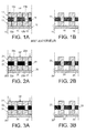
- the contacting (symbolized by the black arrows on the Figure 1A ) of the structure with an agent capable of degrading the sacrificial material causes the degradation of the second layer 11 'of sacrificial material and, following the diffusion of the attacking agent through the permeable membrane 13, that of the first layer 11 of sacrificial material. It is then sufficient to remove the etching agent from the structure (with all the degradation residues it contains), for example with supercritical carbon dioxide, so that the cavities initially filled with sacrificial material become air cavities, as shown on the Figure 1B .
- the permeable membranes currently used are generally polymer membranes.
- these membranes can be infiltrated by the different chemicals that are used during the manufacture of microstructures and, in particular, during etching, "stripping", cleaning and depositing operations. metals necessary for the realization of metal lines, which tends to weaken these membranes and exposes them to a serious risk of degradation.
- the membrane which is integrated in the microstructure is a membrane which is impervious but which can be made later permeable by subjecting it to the action of an etching agent which is also capable of act on the sacrificial material to degrade it.
- the impermeable membrane consists of a single material, to which this material preferably comprises silicon, carbon, hydrogen, oxygen and, optionally, nitrogen and / or fluorine, with a majority of silicon-carbon bonds and a proportion of bonds silicon-oxygen such that the oxygen present in said material represents at most 30% in number of atoms.
- such a membrane can be made permeable under the action of an etching agent capable of selectively destroying the silicon-oxygen bonds it contains (that is to say without affecting the other bonds and, in particular, the silicon-carbon, silicon-hydrogen and carbon-hydrogen bonds) and, consequently, to confer an open porosity on its entire thickness, which is particularly the case of an aqueous solution of hydrofluoric acid.
- an etching agent capable of selectively destroying the silicon-oxygen bonds it contains (that is to say without affecting the other bonds and, in particular, the silicon-carbon, silicon-hydrogen and carbon-hydrogen bonds) and, consequently, to confer an open porosity on its entire thickness, which is particularly the case of an aqueous solution of hydrofluoric acid.
- a material comprises a majority of silicon-carbon bonds when more than 50% of the bonds made by the silicon atoms present in this material are silicon-carbon bonds.
- the material comprising silicon, carbon, hydrogen, oxygen and, optionally, nitrogen and / or fluorine is preferably of the Si v C w H y type. O z or Si v C w N x H y O z with v, w, x, y and z all different from 0.
- Membranes made of a material of this type can be formed in particular by the plasma-assisted chemical vapor deposition technique, better known under the acronym PECVD for " P lasma E nhanced C hemical V apor D eposition".
- PECVD plasma-assisted chemical vapor deposition technique
- v C w H y O z preferably a plasma containing an organosilicon first precursor free of oxygen and a second precursor consisting of oxygen, alone or in combination with carbon and / or hydrogen, while, to obtain a membrane of Si v C w N x H y O z type , it is preferred to add to this plasma a third precursor consisting of nitrogen, alone or in combination with hydrogen and / or carbon.
- the first precursor may be an alkylsilane such as dimethylsilane, trimethylsilane or else tetramethylsilane;
- the second precursor may be oxygen or carbon dioxide, while the third precursor may be nitrogen or ammonia.
- the proportions of the various precursors in the plasma are suitably chosen so that the atomic concentration of oxygen is less than 30% in the membrane.
- a membrane of the type Si v C w H y O z with a plasma containing only one precursor consisting of silicon, carbon, hydrogen and oxygen, but having an oxygen content of less than or equal to 30 at%, such as, for example, diethoxymethylsilane or octamethylcyclotetrasiloxane.
- a membrane of the type Si v C w N x H y O z using this precursor together with another precursor consisting of nitrogen, alone or in combination with hydrogen and / or carbon.
- the plasma may, in addition, contain one or more inert carrier gases, in particular helium and / or argon.
- the formation of the impermeable membrane by PECVD can in particular be carried out in a capacitively coupled reactor.
- the operating parameters are then, preferably, the following: a 13.56 MHz radiofrequency type excitation; a power between 100 and 900 W, a temperature of between 100 and 450 ° C, for a pressure of between 1 and 10 torr (0.133 to 1.33 kPa) and precursor flow rates of between 1 and 10000 cm 3 / minute .
- the characteristics of the membrane and, in particular, its atomic concentration in oxygen can be verified by composition analysis methods such as infrared spectroscopy in transmission.
- the impermeable membrane consists of a matrix comprising at least a first material resistant to the etching agent and in which at least one second material is dispersed. degradable by said etchant.
- the first material is preferably a material which comprises silicon, carbon, hydrogen and, optionally, nitrogen and / or fluorine, but which is free of oxygen.
- the first material is of the type Si v C w H y with v, w and y all different from 0, including obtaining in a dense form, in particular PECVD from pairs of precursors of the trimethylsilane / helium type or silane / methane, is now perfectly controlled.
- the second material it is preferably silicon oxide which is one of the sacrificial materials most used in microelectronics.
- this silicon oxide be present in the matrix in the form of through-going nanowires, that is to say nanowires that extend from one surface to the other of this matrix, and whose degradation by the etching agent will have the effect of creating diffusion channels from one surface to the other of said matrix.
- These silicon oxide nanowires preferably have a diameter ranging from a few nm to some ten nm, and more preferably from 2 nm to 10 nm.
- Silicon oxide nanowires can be formed by numerous techniques and, in particular, by chemical vapor deposition (CVD), catalytic thermal decomposition, also known under the acronym CCVD for "Catalytic Chemical Vapor Deposition", or by the sol-gel route.
- CVD chemical vapor deposition
- CCVD catalytic thermal decomposition
- sol-gel route sol-gel route
- the matrix is formed, preferably by PECVD.
- this technique allows the realization of deposits at low pressures, it allows to cover these nanowires, over their entire length, with the constituent material or materials of the matrix, it being understood that we will take care to adjust the duration of the deposit of so that the ends of the nanowires are not included in the matrix and can thus remain accessible to the etching agent.
- the silicon oxide may also be present in the matrix in the form of inclusions, for example using a PECVD or spin-depositing pore-forming approach, also known in the English terminology as "spin coating".
- the impermeable membrane has a thickness ranging from 10 nm to 10 ⁇ m and, more preferably, from 100 nm to 1 ⁇ m.
- the sacrificial material be silicon oxide and that the etchant be a fluid containing hydrofluoric acid.
- this fluid is preferably an aqueous or organic solution containing 1 or a few% (v / v) of hydrofluoric acid, in which case step b) can be carried out by simply dipping the microstructure in this solution.
- hydrofluoric acid gas pure or mixed with a carrier gas such as nitrogen, or a mixture of hydrofluoric acid and supercritical carbon dioxide, for example in a ratio of 1 / 100 (v / v).
- step c it can be carried out conventionally, that is to say by immersion in deionized water followed by drying, for example at 100 ° C. for 30 minutes.
- the method of the invention has many advantages, in particular that of solving all the problems posed by the integration of permeable membranes, previously mentioned.
- Figures 2A and 2B illustrate in a schematic form a first embodiment of the method of the invention for producing air cavities in an interconnection structure for an integrated circuit.
- the sacrificial material is silicon oxide while the impermeable membrane is a membrane of Si v C w N x H y O z (with v, w, x, y and z all different from 0) which has an oxygen content of the order of 10 atomic% and a thickness of 200 nm.
- a second level of interconnections comprising metallic lines 22c and 22d embedded in a second layer 21 'of SiO 2 , these lines being connected, is produced on the membrane 23, again along a conventional road. respectively to the metal lines 22a and 22b via sleepers 24.
- the structure is immersed in a 1% (v / v) aqueous solution of hydrofluoric acid for 20 minutes, which has the effect of degrading the layer 21 'of SiO 2 of the second level of interconnections, to make the permeable membrane 23 by selective destruction of the Si-O bonds it contains, then degrade the SiO 2 layer 21 of the first level of interconnections.
- the hydrofluoric acid treatment time is determined as a function of the thickness of the layer 21 (about 1 minute for 10 nm) and counting 5 minutes of treatment for the degradation of the Si-O bonds of the membrane 23.
- FIGS. 3A and 3B illustrate in a schematic form a second example of implementation of the method of the invention for producing air cavities in an interconnection structure for an integrated circuit, which differs of that described in Example 1 that by the nature of the impermeable membrane that is integrated into the structure.
- the impermeable membrane 33 consists of a matrix of amorphous hydrogenated silicon carbide (a-SiC: H), 200 nm thick and in which are dispersed through SiO 2 nanowires.
- a-SiC amorphous hydrogenated silicon carbide
- the SiO 2 nanowires are first formed on the first level of interconnections of the structure.
- a first solution is prepared by gradually adding 52 ml of tetraethylorthosilicate (TEOS) to 115 ml of ethanol and a second solution by mixing 115 ml of ethanol with 18 ml of water and 0.27 ml of acid. hydrochloric. The second solution is then added to the first. The resulting mixture is spread by centrifugation on the first level of interconnections and the structure is placed in a heated enclosure (200 ° C) for 12 hours.
- TEOS tetraethylorthosilicate
- the membrane thus formed is then subjected to chemical-mechanical polishing for 10 seconds, using a basic aqueous suspension (pH 8) of colloidal silica particles and using a speed of rotation of the plate of 80 revolutions / min. pressure of 2 psi (13.789 kPa).
Landscapes
- Engineering & Computer Science (AREA)
- Manufacturing & Machinery (AREA)
- Microelectronics & Electronic Packaging (AREA)
- Internal Circuitry In Semiconductor Integrated Circuit Devices (AREA)
- Weting (AREA)
- Formation Of Insulating Films (AREA)
- Micromachines (AREA)
Applications Claiming Priority (1)
| Application Number | Priority Date | Filing Date | Title |
|---|---|---|---|
| FR0850249A FR2926294B1 (fr) | 2008-01-16 | 2008-01-16 | Procede de realisation de cavites d'air dans des microstructures |
Publications (2)
| Publication Number | Publication Date |
|---|---|
| EP2080734A1 true EP2080734A1 (de) | 2009-07-22 |
| EP2080734B1 EP2080734B1 (de) | 2011-03-02 |
Family
ID=39773177
Family Applications (1)
| Application Number | Title | Priority Date | Filing Date |
|---|---|---|---|
| EP09150388A Not-in-force EP2080734B1 (de) | 2008-01-16 | 2009-01-12 | Herstellungsverfahren von Lufthohlräumen in Mikrostrukturen |
Country Status (5)
| Country | Link |
|---|---|
| US (1) | US8231797B2 (de) |
| EP (1) | EP2080734B1 (de) |
| JP (1) | JP2009188398A (de) |
| DE (1) | DE602009000787D1 (de) |
| FR (1) | FR2926294B1 (de) |
Families Citing this family (7)
| Publication number | Priority date | Publication date | Assignee | Title |
|---|---|---|---|---|
| JP4464125B2 (ja) * | 2003-12-22 | 2010-05-19 | ソニー株式会社 | 構造体の作製方法及びシリコン酸化膜エッチング剤 |
| FR3006684B1 (fr) * | 2013-06-07 | 2016-10-21 | Commissariat Energie Atomique | Procede de traitement d'une surface et dispositif mis en œuvre |
| US10815584B2 (en) | 2013-11-15 | 2020-10-27 | National University Of Singapore | Ordered growth of large crystal graphene by laser-based localized heating for high throughput production |
| US10683586B2 (en) | 2014-02-04 | 2020-06-16 | National University Of Singapore | Method of pulsed laser-based large area graphene synthesis on metallic and crystalline substrates |
| US11848037B2 (en) | 2015-07-29 | 2023-12-19 | National University Of Singapore | Method of protecting a magnetic layer of a magnetic recording medium |
| KR102222037B1 (ko) * | 2019-04-05 | 2021-03-04 | 주식회사 필옵틱스 | 에어 갭을 갖는 반도체 소자 및 그 제조 방법 |
| KR102196500B1 (ko) * | 2019-07-17 | 2020-12-30 | 주식회사 필옵틱스 | 공정 신뢰성을 확보한 에어 갭 구조 반도체 소자 및 그 제조 방법 |
Citations (4)
| Publication number | Priority date | Publication date | Assignee | Title |
|---|---|---|---|---|
| US20020022378A1 (en) * | 2000-07-10 | 2002-02-21 | Mikhail Baklanov | Method to produce a porous oxygen-silicon layer |
| US6387818B1 (en) * | 2000-07-21 | 2002-05-14 | Advanced Micro Devices, Inc. | Method of porous dielectric formation with anodic template |
| DE10355395A1 (de) | 2003-11-25 | 2005-06-30 | Robert Bosch Gmbh | Verfahren zur Herstellung eines mikrostrukturierten Bauelementes und hierdurch hergestelltes mikrostrukturiertes Bauelement |
| EP1739737A1 (de) * | 2005-06-13 | 2007-01-03 | Infineon Technologies AG | Herstellung von Strukturen mit Luft als Dielektrikum |
Family Cites Families (9)
| Publication number | Priority date | Publication date | Assignee | Title |
|---|---|---|---|---|
| JPH05283542A (ja) * | 1992-03-31 | 1993-10-29 | Mitsubishi Electric Corp | 半導体集積回路装置及びその製造方法 |
| JP2000340651A (ja) * | 1999-05-28 | 2000-12-08 | Hitachi Chem Co Ltd | 低誘電率膜の製造法 |
| US6204165B1 (en) * | 1999-06-24 | 2001-03-20 | International Business Machines Corporation | Practical air dielectric interconnections by post-processing standard CMOS wafers |
| JP3365554B2 (ja) * | 2000-02-07 | 2003-01-14 | キヤノン販売株式会社 | 半導体装置の製造方法 |
| JP3745257B2 (ja) * | 2001-08-17 | 2006-02-15 | キヤノン販売株式会社 | 半導体装置及びその製造方法 |
| KR100422597B1 (ko) * | 2001-11-27 | 2004-03-16 | 주식회사 하이닉스반도체 | 다마신 공정에 의해 형성된 캐패시터와 금속배선을 가지는반도체소자 |
| JP4068072B2 (ja) * | 2003-01-29 | 2008-03-26 | Necエレクトロニクス株式会社 | 半導体装置及びその製造方法 |
| TW200746355A (en) * | 2005-07-12 | 2007-12-16 | St Microelectronics Crolles 2 | Integration control and reliability enhancement of interconnect air cavities |
| JP5272336B2 (ja) * | 2007-06-21 | 2013-08-28 | 東京エレクトロン株式会社 | 半導体装置の製造方法、プラズマエッチング方法及びプラズマエッチング装置 |
-
2008
- 2008-01-16 FR FR0850249A patent/FR2926294B1/fr not_active Expired - Fee Related
-
2009
- 2009-01-12 DE DE602009000787T patent/DE602009000787D1/de active Active
- 2009-01-12 EP EP09150388A patent/EP2080734B1/de not_active Not-in-force
- 2009-01-14 US US12/353,872 patent/US8231797B2/en not_active Expired - Fee Related
- 2009-01-15 JP JP2009007011A patent/JP2009188398A/ja active Pending
Patent Citations (4)
| Publication number | Priority date | Publication date | Assignee | Title |
|---|---|---|---|---|
| US20020022378A1 (en) * | 2000-07-10 | 2002-02-21 | Mikhail Baklanov | Method to produce a porous oxygen-silicon layer |
| US6387818B1 (en) * | 2000-07-21 | 2002-05-14 | Advanced Micro Devices, Inc. | Method of porous dielectric formation with anodic template |
| DE10355395A1 (de) | 2003-11-25 | 2005-06-30 | Robert Bosch Gmbh | Verfahren zur Herstellung eines mikrostrukturierten Bauelementes und hierdurch hergestelltes mikrostrukturiertes Bauelement |
| EP1739737A1 (de) * | 2005-06-13 | 2007-01-03 | Infineon Technologies AG | Herstellung von Strukturen mit Luft als Dielektrikum |
Also Published As
| Publication number | Publication date |
|---|---|
| FR2926294A1 (fr) | 2009-07-17 |
| FR2926294B1 (fr) | 2010-08-13 |
| US8231797B2 (en) | 2012-07-31 |
| US20090178999A1 (en) | 2009-07-16 |
| JP2009188398A (ja) | 2009-08-20 |
| DE602009000787D1 (de) | 2011-04-14 |
| EP2080734B1 (de) | 2011-03-02 |
Similar Documents
| Publication | Publication Date | Title |
|---|---|---|
| EP2080734B1 (de) | Herstellungsverfahren von Lufthohlräumen in Mikrostrukturen | |
| EP2081217B1 (de) | Herstellungsverfahren von Folien aus amorphem hydrogenisiertem Siliziumkarbid, das über durchlässige Poren verfügt | |
| EP0780889B1 (de) | Verfahren zur selektiven Abscheidung von Siliciden hochschmelzender Metalle auf Silizium | |
| EP1902463A1 (de) | Verfahren zur verringerung der rauhigkeit einer dicken isolationsschicht | |
| FR2982281A1 (fr) | Procede de synthese d'un feuillet de graphene sur un siliciure de platine, structures obtenues par ce procede et leurs utilisations | |
| FR3000602A1 (fr) | Procede de gravure d'un materiau dielectrique poreux | |
| FR2913816A1 (fr) | Procede de fabrication d'une structure d'interconnexions a cavites pour circuit integre | |
| FR2931015A1 (fr) | Procede de realisation de cavites d'air dans des microstructures, notamment du type structures d'interconnexions a cavites d'air pour circuit integre | |
| EP1816674A1 (de) | Verfahren zur anisotropen Ätzung | |
| EP1030353A1 (de) | Anisotropes Plasmaätzen von dielektrischen, organisch- polymeren Materialien | |
| FR2951581A1 (fr) | Procede de fabrication d'un film multicouche comprenant au moins une couche ultra mince de silicium cristallin et dispositifs obtenus par ce procede | |
| EP2019152B1 (de) | Herstellungsverfahren von Dünnschichten aus nanoporösen dielektrischen Materialien | |
| EP2138457B1 (de) | Verfahren zur Herstellung einer Matte aus Kohlenstoffnanoröhren auf einem Leiter- oder Halbleitersubstrat | |
| EP2081216B1 (de) | Verfahren zur Herstellung von durchlässigen dielektrischen Folien | |
| FR2855324A1 (fr) | Procede de fabrication d'une interconnexion pour un dispositif a semiconducteur | |
| EP2263253A2 (de) | Verfahren zur formung eines porösen materials in einem mikrohohlraum oder einem mikrodurchgang durch mechanochemisches polieren | |
| EP2747140B1 (de) | Verfahren zur Herstellung mindestens eines Nanoelements auf Siliziumbasis in einer Siliziumoxydschicht, und Herstellungsverfahren einer Vorrichtung mit mindestens einem solchen Nanoelement. | |
| EP4213182B1 (de) | Verfahren zur aktivierung einer belichteten schicht | |
| CN104167405A (zh) | 一种集成电路及其制备方法 | |
| WO2025140983A1 (fr) | Procédé de collage direct entre deux substrats | |
| EP4035773A1 (de) | Verfahren zur bildung eines metallorganischen netzes | |
| FR2910178A1 (fr) | Procede de realisation d'un element dielectrique poreux et element dielectrique correspondant | |
| FR2931167A1 (fr) | Procede de fabrication d'une membrane dielectrique permeable a au moins un agent d'attaque chimique utilisable pour realiser des cavites d'air dans des dispositifs electroniques. | |
| FR3114992A1 (fr) | Dispositif comportant une membrane de graphène | |
| FR2795746A1 (fr) | Procede de depot d'un materiau dielectrique a base de silicium sur du cuivre |
Legal Events
| Date | Code | Title | Description |
|---|---|---|---|
| PUAI | Public reference made under article 153(3) epc to a published international application that has entered the european phase |
Free format text: ORIGINAL CODE: 0009012 |
|
| AK | Designated contracting states |
Kind code of ref document: A1 Designated state(s): AT BE BG CH CY CZ DE DK EE ES FI FR GB GR HR HU IE IS IT LI LT LU LV MC MK MT NL NO PL PT RO SE SI SK TR |
|
| AX | Request for extension of the european patent |
Extension state: AL BA RS |
|
| 17P | Request for examination filed |
Effective date: 20091223 |
|
| 17Q | First examination report despatched |
Effective date: 20100122 |
|
| AKX | Designation fees paid |
Designated state(s): DE FR GB IT |
|
| RAP1 | Party data changed (applicant data changed or rights of an application transferred) |
Owner name: COMMISSARIAT A L'ENERGIE ATOMIQUE ET AUX ENERGIES |
|
| GRAP | Despatch of communication of intention to grant a patent |
Free format text: ORIGINAL CODE: EPIDOSNIGR1 |
|
| GRAS | Grant fee paid |
Free format text: ORIGINAL CODE: EPIDOSNIGR3 |
|
| GRAA | (expected) grant |
Free format text: ORIGINAL CODE: 0009210 |
|
| AK | Designated contracting states |
Kind code of ref document: B1 Designated state(s): DE FR GB IT |
|
| REG | Reference to a national code |
Ref country code: GB Ref legal event code: FG4D Free format text: NOT ENGLISH |
|
| REF | Corresponds to: |
Ref document number: 602009000787 Country of ref document: DE Date of ref document: 20110414 Kind code of ref document: P |
|
| REG | Reference to a national code |
Ref country code: DE Ref legal event code: R096 Ref document number: 602009000787 Country of ref document: DE Effective date: 20110414 |
|
| PLBE | No opposition filed within time limit |
Free format text: ORIGINAL CODE: 0009261 |
|
| STAA | Information on the status of an ep patent application or granted ep patent |
Free format text: STATUS: NO OPPOSITION FILED WITHIN TIME LIMIT |
|
| 26N | No opposition filed |
Effective date: 20111205 |
|
| REG | Reference to a national code |
Ref country code: DE Ref legal event code: R097 Ref document number: 602009000787 Country of ref document: DE Effective date: 20111205 |
|
| PGFP | Annual fee paid to national office [announced via postgrant information from national office to epo] |
Ref country code: IT Payment date: 20120131 Year of fee payment: 4 |
|
| PGFP | Annual fee paid to national office [announced via postgrant information from national office to epo] |
Ref country code: GB Payment date: 20150114 Year of fee payment: 7 |
|
| REG | Reference to a national code |
Ref country code: FR Ref legal event code: PLFP Year of fee payment: 8 |
|
| PGFP | Annual fee paid to national office [announced via postgrant information from national office to epo] |
Ref country code: DE Payment date: 20160108 Year of fee payment: 8 |
|
| PGFP | Annual fee paid to national office [announced via postgrant information from national office to epo] |
Ref country code: FR Payment date: 20160201 Year of fee payment: 8 |
|
| PG25 | Lapsed in a contracting state [announced via postgrant information from national office to epo] |
Ref country code: IT Free format text: LAPSE BECAUSE OF NON-PAYMENT OF DUE FEES Effective date: 20140112 |
|
| GBPC | Gb: european patent ceased through non-payment of renewal fee |
Effective date: 20160112 |
|
| PG25 | Lapsed in a contracting state [announced via postgrant information from national office to epo] |
Ref country code: GB Free format text: LAPSE BECAUSE OF NON-PAYMENT OF DUE FEES Effective date: 20160112 |
|
| REG | Reference to a national code |
Ref country code: DE Ref legal event code: R119 Ref document number: 602009000787 Country of ref document: DE |
|
| REG | Reference to a national code |
Ref country code: FR Ref legal event code: ST Effective date: 20170929 |
|
| PG25 | Lapsed in a contracting state [announced via postgrant information from national office to epo] |
Ref country code: FR Free format text: LAPSE BECAUSE OF NON-PAYMENT OF DUE FEES Effective date: 20170131 |
|
| PG25 | Lapsed in a contracting state [announced via postgrant information from national office to epo] |
Ref country code: DE Free format text: LAPSE BECAUSE OF NON-PAYMENT OF DUE FEES Effective date: 20170801 |