EP2081180A2 - Dispositif d'affichage électroluminescent organique - Google Patents
Dispositif d'affichage électroluminescent organique Download PDFInfo
- Publication number
- EP2081180A2 EP2081180A2 EP09250125A EP09250125A EP2081180A2 EP 2081180 A2 EP2081180 A2 EP 2081180A2 EP 09250125 A EP09250125 A EP 09250125A EP 09250125 A EP09250125 A EP 09250125A EP 2081180 A2 EP2081180 A2 EP 2081180A2
- Authority
- EP
- European Patent Office
- Prior art keywords
- light emitting
- organic light
- emitting display
- power source
- pixel
- Prior art date
- Legal status (The legal status is an assumption and is not a legal conclusion. Google has not performed a legal analysis and makes no representation as to the accuracy of the status listed.)
- Ceased
Links
- 238000000034 method Methods 0.000 claims description 12
- 230000008878 coupling Effects 0.000 claims 1
- 238000010168 coupling process Methods 0.000 claims 1
- 238000005859 coupling reaction Methods 0.000 claims 1
- 101001045744 Sus scrofa Hepatocyte nuclear factor 1-beta Proteins 0.000 description 9
- 239000003990 capacitor Substances 0.000 description 7
- 238000010586 diagram Methods 0.000 description 4
- 230000007547 defect Effects 0.000 description 1
- 238000012986 modification Methods 0.000 description 1
- 230000004048 modification Effects 0.000 description 1
- 239000002365 multiple layer Substances 0.000 description 1
- 238000005215 recombination Methods 0.000 description 1
- 230000006798 recombination Effects 0.000 description 1
- 239000002356 single layer Substances 0.000 description 1
Images

Classifications
-
- G—PHYSICS
- G09—EDUCATION; CRYPTOGRAPHY; DISPLAY; ADVERTISING; SEALS
- G09G—ARRANGEMENTS OR CIRCUITS FOR CONTROL OF INDICATING DEVICES USING STATIC MEANS TO PRESENT VARIABLE INFORMATION
- G09G3/00—Control arrangements or circuits, of interest only in connection with visual indicators other than cathode-ray tubes
- G09G3/20—Control arrangements or circuits, of interest only in connection with visual indicators other than cathode-ray tubes for presentation of an assembly of a number of characters, e.g. a page, by composing the assembly by combination of individual elements arranged in a matrix no fixed position being assigned to or needed to be assigned to the individual characters or partial characters
- G09G3/22—Control arrangements or circuits, of interest only in connection with visual indicators other than cathode-ray tubes for presentation of an assembly of a number of characters, e.g. a page, by composing the assembly by combination of individual elements arranged in a matrix no fixed position being assigned to or needed to be assigned to the individual characters or partial characters using controlled light sources
- G09G3/30—Control arrangements or circuits, of interest only in connection with visual indicators other than cathode-ray tubes for presentation of an assembly of a number of characters, e.g. a page, by composing the assembly by combination of individual elements arranged in a matrix no fixed position being assigned to or needed to be assigned to the individual characters or partial characters using controlled light sources using electroluminescent panels
- G09G3/32—Control arrangements or circuits, of interest only in connection with visual indicators other than cathode-ray tubes for presentation of an assembly of a number of characters, e.g. a page, by composing the assembly by combination of individual elements arranged in a matrix no fixed position being assigned to or needed to be assigned to the individual characters or partial characters using controlled light sources using electroluminescent panels semiconductive, e.g. using light-emitting diodes [LED]
- G09G3/3208—Control arrangements or circuits, of interest only in connection with visual indicators other than cathode-ray tubes for presentation of an assembly of a number of characters, e.g. a page, by composing the assembly by combination of individual elements arranged in a matrix no fixed position being assigned to or needed to be assigned to the individual characters or partial characters using controlled light sources using electroluminescent panels semiconductive, e.g. using light-emitting diodes [LED] organic, e.g. using organic light-emitting diodes [OLED]
-
- H—ELECTRICITY
- H05—ELECTRIC TECHNIQUES NOT OTHERWISE PROVIDED FOR
- H05B—ELECTRIC HEATING; ELECTRIC LIGHT SOURCES NOT OTHERWISE PROVIDED FOR; CIRCUIT ARRANGEMENTS FOR ELECTRIC LIGHT SOURCES, IN GENERAL
- H05B33/00—Electroluminescent light sources
- H05B33/02—Details
- H05B33/06—Electrode terminals
-
- H—ELECTRICITY
- H10—SEMICONDUCTOR DEVICES; ELECTRIC SOLID-STATE DEVICES NOT OTHERWISE PROVIDED FOR
- H10K—ORGANIC ELECTRIC SOLID-STATE DEVICES
- H10K59/00—Integrated devices, or assemblies of multiple devices, comprising at least one organic light-emitting element covered by group H10K50/00
- H10K59/10—OLED displays
- H10K59/12—Active-matrix OLED [AMOLED] displays
- H10K59/131—Interconnections, e.g. wiring lines or terminals
-
- G—PHYSICS
- G09—EDUCATION; CRYPTOGRAPHY; DISPLAY; ADVERTISING; SEALS
- G09G—ARRANGEMENTS OR CIRCUITS FOR CONTROL OF INDICATING DEVICES USING STATIC MEANS TO PRESENT VARIABLE INFORMATION
- G09G2300/00—Aspects of the constitution of display devices
- G09G2300/04—Structural and physical details of display devices
- G09G2300/0421—Structural details of the set of electrodes
- G09G2300/0426—Layout of electrodes and connections
-
- G—PHYSICS
- G09—EDUCATION; CRYPTOGRAPHY; DISPLAY; ADVERTISING; SEALS
- G09G—ARRANGEMENTS OR CIRCUITS FOR CONTROL OF INDICATING DEVICES USING STATIC MEANS TO PRESENT VARIABLE INFORMATION
- G09G2320/00—Control of display operating conditions
- G09G2320/02—Improving the quality of display appearance
- G09G2320/0223—Compensation for problems related to R-C delay and attenuation in electrodes of matrix panels, e.g. in gate electrodes or on-substrate video signal electrodes
-
- G—PHYSICS
- G09—EDUCATION; CRYPTOGRAPHY; DISPLAY; ADVERTISING; SEALS
- G09G—ARRANGEMENTS OR CIRCUITS FOR CONTROL OF INDICATING DEVICES USING STATIC MEANS TO PRESENT VARIABLE INFORMATION
- G09G2320/00—Control of display operating conditions
- G09G2320/02—Improving the quality of display appearance
- G09G2320/0233—Improving the luminance or brightness uniformity across the screen
-
- G—PHYSICS
- G09—EDUCATION; CRYPTOGRAPHY; DISPLAY; ADVERTISING; SEALS
- G09G—ARRANGEMENTS OR CIRCUITS FOR CONTROL OF INDICATING DEVICES USING STATIC MEANS TO PRESENT VARIABLE INFORMATION
- G09G3/00—Control arrangements or circuits, of interest only in connection with visual indicators other than cathode-ray tubes
- G09G3/20—Control arrangements or circuits, of interest only in connection with visual indicators other than cathode-ray tubes for presentation of an assembly of a number of characters, e.g. a page, by composing the assembly by combination of individual elements arranged in a matrix no fixed position being assigned to or needed to be assigned to the individual characters or partial characters
-
- H—ELECTRICITY
- H10—SEMICONDUCTOR DEVICES; ELECTRIC SOLID-STATE DEVICES NOT OTHERWISE PROVIDED FOR
- H10K—ORGANIC ELECTRIC SOLID-STATE DEVICES
- H10K50/00—Organic light-emitting devices
- H10K50/80—Constructional details
- H10K50/87—Arrangements for heating or cooling
-
- H—ELECTRICITY
- H10—SEMICONDUCTOR DEVICES; ELECTRIC SOLID-STATE DEVICES NOT OTHERWISE PROVIDED FOR
- H10K—ORGANIC ELECTRIC SOLID-STATE DEVICES
- H10K59/00—Integrated devices, or assemblies of multiple devices, comprising at least one organic light-emitting element covered by group H10K50/00
- H10K59/80—Constructional details
- H10K59/8794—Arrangements for heating and cooling
Definitions
- the present invention relates to a process and an organic light emitting display device, and more particularly, to a process for fabricating an organic light emitting display device capable of minimizing an IR drop of pixel power sources supplied to an organic light emitting display panel and an organic light emitting display device capable of minimizing an IR drop of pixel power sources supplied to an organic light emitting display panel.
- organic light emitting display devices display images using organic light emitting diodes (OLED) that generate lights by the recombination of electrons and holes. Since the organic light emitting display device has higher response speed and is driven with lower power consumption, the organic light emitting display device is spotlighted as a next generation display.
- OLED organic light emitting diodes
- the organic light emitting display device includes a pixel unit including a plurality of pixels, driving circuits for supplying driving signals to the pixel unit, and a power source supplying circuit for supplying pixel power sources to the pixel unit.
- the pixels emit lights with brightness corresponding to data signals supplied in synchronization with scan signals when the scan signals are supplied. Therefore, the organic light emitting display panel displays a predetermined image.
- the brightness of the emitted lights of the pixels is affected by the voltage of the pixel power sources. That is, the pixel power sources determine the brightness of the emitted lights of the pixels together with the data signals.
- the pixel power sources having an identical voltage level are supplied to the pixels respectively.
- the pixel power sources however are direct current (DC) power sources having a predetermined voltage level and IR drop may be generated while passing through a power source line.
- the IR drop is a voltage drop associated with an electrical resistance (R) of a power source line or an electrical current flow (I), and is the product of the electrical current (in amperes) and the electrical resistance (in ohms).
- brightness deviation between the pixels may be increased in accordance with the distance between the pixels and a power source pad that receives the pixel power sources.
- an organic light emitting display device may be constructed with an organic light emitting display panel having a first side on which an image is displayed, a second side that faces the first side and, a plurality of first and second power source pads provided at two or more edges of the second side to receive first and second pixel power sources in at least two directions and a pixel power source supplying flexible printed circuit board (FPCB) provided on the second side of the organic light emitting display panel to provide a plurality of pads electrically coupled to the first and second power source pads and to supply the first and second pixel power sources to the organic light emitting display panel.
- FPCB flexible printed circuit board
- the first power source pads may be formed at a first edge region of the second side and a second edge region that faces the first edge region and the second power source pads may be formed at a third edge region of the second side and a fourth edge region that faces the third edge region.
- the first power source pads may be formed in the first and second edge regions and the second power source pads may be formed in the third and fourth edge regions.
- the first power source pads and the second power source pads may be formed at different edges of the second side of the organic light emitting display panel.
- the first and second power source pads may receive the first and second pixel power sources in two directions that face each other of the pixel power source supplying FPCB.
- a pixel unit that receives the first and second pixel power sources from the first and second power source pads may be positioned at the center of the organic light emitting display panel and a plurality of signal pads for supplying driving signals to the pixel unit may be formed between the first and second power source pads.
- the signal pads may be electrically coupled to driving FPCBs provided in addition to the pixel power source supplying FPCB to transmit the driving signals supplied from the driving FPCBs to the pixel unit.
- the driving FPCBs may be plural.
- at least one of a scan driver and a data driver may be mounted on the driving FPCBs so that at least one of the scan signals and the data signals may be supplied to the pixel unit.
- the pixel power source supplying FPCB may be provided to overlap the pixel unit and the pads of the pixel power source supplying FPCB may be formed to overlap the first and second power source pads.
- At least one aperture may be formed in at least one region of the pixel power source supplying FPCB.
- FIG. 1 is a block diagram illustrating an example of an organic light emitting display device constructed as an embodiment of the principle of the present invention
- FIG. 2 is a circuit diagram illustrating an example of one pixel illustrated by FIG. 1 ;
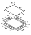
- FIG. 3 is an exploded perspective view of an organic light emitting display panel and a flexible panel circuit board (FPCB) for supplying power sources to pixels constructed as an embodiment of the present invention
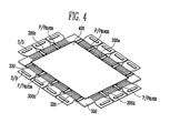
- FIG. 4 is a coupled perspective view of the assembled organic light emitting display device of FIG. 3 and the FPCB for supplying power sources to pixels;
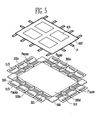
- FIG. 5 is an exploded perspective view of an organic light emitting display panel device constructed as another embodiment of the present invention and the FPCB for supplying power sources to pixels.
- first element when a first element is described as being coupled to a second element, the first element may be not only directly coupled to the second element but may also be indirectly coupled to the second element via a third element. Further, some of the elements that are not essential to the complete understanding of the invention are omitted for clarity. Also, like reference numerals refer to like elements throughout.
- FIG. 1 is a block diagram illustrating an example of an organic light emitting display device constructed according to the present invention.
- an organic light emitting display device 100 includes a scan driver 110, a data driver 120, a timing controller 140, a pixel unit 150, and a power source supplying unit 130.
- Scan driver 110 generates scan signals to correspond to scan driving control signals SCS supplied from timing controller 140.
- the scan signals generated by scan driver 110 are sequentially supplied to scan lines S 1 to Sn.
- Data driver 120 generates data signals to correspond to data Data and data driving control signals DCS supplied from timing controller 140.
- the data signals generated by data driver 120 are supplied to data lines D1 to Dm in synchronization with the scan signals.
- Timing controller 140 generates the scan driving control signals SCS and the data driving control signals DCS in response to synchronizing signals supplied from the exterior.
- the scan driving control signals SCS generated by timing controller 140 are supplied to scan driver 110 and the data driving control signals DCS are supplied to data driver 120.
- timing controller 140 transmits the data Data supplied from the exterior to data driver 120.
- Pixel unit 150 includes a plurality of pixels 160 formed in regions partitioned off by the scan lines S1 to Sn and the data lines D 1 to Dm. Pixel unit 150 displays an image to correspond to the scan signals supplied from scan driver 110 and the data signals supplied from data driver 120.
- Power source supplying unit 130 generates first and second pixel power sources ELVDD and ELVSS using an external power source supplied from an external power source supplying apparatus (not shown). Then, power source supplying unit 130 supplies the generated first and second pixel power sources ELVDD and ELVSS to pixel unit 150.
- pixel unit 150 is formed in the organic light emitting display panel.
- Scan driver 110 and/or data driver 120 are/is mounted on the organic light emitting display panel or an additional flexible printed circuit board (FPCB). Scan driver 110 and/or data driver 120 may be electrically coupled to the organic light emitting display panel through a pad unit.
- FPCB flexible printed circuit board
- power source supplying unit 130 and/or timing controller 140 are/is mounted on a driving board outside the organic light emitting display panel to be electrically coupled to the organic light emitting display panel and/or the driving FPCBs through the FPCB.
- FIG. 2 is a circuit diagram illustrating an example of the pixel of FIG. 1 .
- a pixel coupled to an nth scan line Sn and an mth data line Dm will be illustrated.
- a pixel 160 includes an organic light emitting diode OLED, the scan line Sn, the data line Dm, a first pixel power source ELVDD, and a pixel circuit 162 coupled to the OLED.
- the anode electrode of the OLED is electrically coupled to pixel circuit 162 and the cathode electrode is electrically coupled to the second pixel power source ELVSS.
- the OLED emits lights with the brightness of the lights corresponding to the amount of electrical current supplied from pixel circuit 162.
- Pixel circuit 162 includes a first transistor M1, a second transistor M2, and a storage capacitor Cst.
- the first electrode of the first transistor M1 is electrically coupled to the data line Dm, and the second electrode of the first transistor M1 is electrically coupled to a first node N1.
- the gate electrode of the first transistor M1 is electrically coupled to the scan line Sn.
- the first transistor M1 is turned on when a scan signal is supplied to the scan line Sn to transmit a data signal supplied to the data line Dm to the first node N1.
- the first electrode of the second transistor M2 is electrically coupled to the first pixel power source ELVDD, and the second electrode of the second transistor M2 is electrically coupled to the anode electrode of the OLED.
- the gate electrode of the second transistor M2 is coupled to the first node N1.
- the second transistor M2 controls electrical current that flows from the first pixel power source ELVDD to the anode electrode of the OLED to correspond to a voltage supplied to the gate electrode of second transistor M2.
- One terminal of a storage capacitor Cst is coupled to the first node N1, and the other terminal of the storage capacitor Cst is coupled to the first pixel power source ELVDD and the first electrode of the second transistor M2.
- the storage capacitor Cst stores a voltage corresponding to a data signal supplied to the first node N1 when the scan signal is supplied to the scan line Sn and maintains the stored voltage in one frame.
- the operation process of pixel 160 will be described in detail.
- the first transistor M1 is turned on.
- the data signal supplied to the data line Dm is transmitted to the first node N1 through the first transistor M1.
- the second transistor M2 controls the electrical current that flows from the first pixel power source ELVDD to the OLED to correspond to a voltage supplied to the gate electrode thereof. Therefore, the OLED emits light with brightness corresponding to the amount of electrical current supplied thereto to enable the display of an image.
- pixel 160 emits lights with brightness corresponding to the amount of current supplied from the second transistor M2.
- the voltage of the first node N1 to which the gate electrode of the second transistor M2 is electrically coupled is maintained in one frame by the storage capacitor Cst.
- the storage capacitor Cst is charged with a voltage corresponding to a difference between the voltage of the first pixel power source ELVDD and the data signal while the data signal is supplied to maintain the voltage in one frame. Therefore, the emission brightness of pixel 160 varies in accordance with the voltage of the first pixel power source ELVDD and the data signal.
- the voltage of the first pixel power source ELVDD supplied to the pixels 160 may vary by the IR drop generated while passing through a power source line. Therefore, pixels 160 that receive the same data signal emit light with different brightness so that picture quality may deteriorate.
- FIG. 3 is an exploded perspective view of an organic light emitting display panel and a flexible panel circuit board (FPCB) for supplying power sources to pixels constructed as an embodiment of the present invention.
- FIG. 4 is a coupled perspective view of the organic light emitting display of FIG. 3 and the FPCB for supplying power sources to pixels.
- the scan driver and/or the data driver are not mounted on the organic light emitting display panel but are mounted on an additional FPCB.
- the present invention is however not limited to these embodiments.
- an organic light emitting display panel 300 includes a pixel unit 310 positioned in the center, a plurality of power source pads P ELVDD and P ELVSS and signal pads 320 positioned at side edges 300a to 300d to supply the pixel power sources ELVDD and ELVSS and driving signals to pixel unit 310.
- Pixel unit 310 includes a plurality of pixels that are not shown. Pixel unit 310 displays an image to correspond to the driving signals supplied from signal pads 320 and the pixel power sources ELVDD and ELVSS supplied from the power source pads P ELVDD and P ELVSS . Pixel unit 310 emits light to the opposite side 312 (hereinafter, a first side of organic light emitting display panel 300) that faces a pixel power source supplying FPCB 400 to display an image.
- the power source pads P ELVDD and P ELVSS are provided at two or more edges of one side 311 (hereinafter, a second side of organic light emitting display panel 300) that faces the first side on which the image is displayed.
- the power source pads P ELVDD and P ELVSS include the first power source pads P ELVDD that receive the first pixel power source ELVDD and the second power source pads P ELVSS that receive the second pixel power source ELVSS.
- the first and second power source pads P ELVDD and P ELVSS are dispersed at two or more edges of second surface 311 of organic light emitting display panel 300 to receive the first and second pixel power sources ELVDD and ELVSS in opposite two directions of the pixel power source supplying FPCB 400.
- the first power source pads P ELVDD may be formed at first and second edges 300a and 300b that face second side 311 of organic light emitting display panel 300. Therefore, the first power source pads P ELVDD can receive the first pixel power source ELVDD in two opposite directions to transmit the first pixel power source ELVDD to pixel unit 310.
- the second power source pads P ELVSS may be formed at third and fourth edges 300c and 300d that face second side 311 of organic light emitting display panel 300. Therefore, the second power source pads P ELVSS can receive the second pixel power source ELVSS in two opposite directions to transmit the second pixel power source ELVSS to pixel unit 310.
- first power source pads P ELVDD and the second power source pads P ELVSS can be formed at different edges of second side 311 of organic light emitting display panel 300.
- the arrangement of the power source pads P ELVDD and P ELVSS according to the principles of the present invention is not limited to the above described features. That is, the first and second power source pads P ELVDD and P ELVSS are provided at three or more regions of second side 311 of organic light emitting display panel 300. Therefore, the first and second power source pads P ELVDD and P ELVSS may receive the first and second pixel power sources ELVDD and ELVSS in the at least three different directions. In this case, at least parts of the first and second power source pads P ELVDD and P ELVSS can be formed at the same edge of second side 311 of organic light emitting display panel 300.
- Signal pads 320 are electrically coupled to driving FPCBs 330 included in addition to pixel power source supplying FPCB 400 to transmit the driving signals supplied from driving FPCBs 330 to pixel unit 310.
- Signal pads 320 are located between the first and second power source pads P ELVDD and P ELVSS .
- the plurality of driving FPCBs 330 electrically coupled to signal pads 320 can be provided.
- the scan driver S/D for supplying the scan signals to pixel unit 310 and/or the data driver D/D for supplying the data signals to pixel unit 310 can be mounted on driving FPCBs 330.
- Pixel power source supplying FPCB 400 is provided on second side 311 of organic light emitting display panel 300.
- Pixel power source supplying FPCB 400 includes a plurality of pads P electrically coupled to the first and second power source pads P ELVDD and P ELVSS of organic light emitting display 300.
- pixel power source supplying FPCB 400 may be formed in the form of a plate to overlap pixel unit 310 to be provided on second side 311 of organic light emitting display panel 300.
- Pads P that overlap the first and second power source pads P ELVDD and P ELVSS of organic light emitting display panel 300 to be electrically coupled to the first and second power source pads P ELVDD and P ELVSS are provided at the edges of pixel power source supplying FPCB 400.
- single-layer or multiple-layer lines for supplying the first and second pixel power sources ELVDD and ELVSS are provided in the pixel power source supplying FPCB 400.
- Pixel power source supplying FPCB 400 is electrically coupled to a power source supplying unit (not shown) mounted on a driving board through an interface to receive the first and second pixel power sources ELVDD and ELVSS. Pixel power source supplying FPCB 400 evenly applies the first and second pixel power sources ELVDD and ELVSS to the organic light emitting display panel 300 through an internal line.
- the power source pads P ELVDD and P ELVSS of organic light emitting display panel 300 are provided at two or more edges so that the first and second pixel power sources ELVDD and ELVSS are supplied to organic light emitting display panel 300 in the at least two different directions.
- organic light emitting display panel 300 it is possible to minimize the IR drop of the first and second pixel power sources ELVDD and ELVSS in organic light emitting display panel 300. Therefore, although the size of organic light emitting display panel 300 may increase, it is possible for the organic light emitting display device to display an image of uniform picture quality. Therefore, the organic light emitting display device may be applied to various displays such as a TV and a sign board.
- Pixel power source supplying FPCB 400 for supplying the first and second pixel power sources ELVDD and ELVSS to the organic light emitting display panel 300 is additionally provided.
- Pixel power source supplying FPCB 400 is formed in the shape of a plate that overlaps pixel unit 310 of organic light emitting display panel 300.
- the first and second pixel power sources ELVDD and ELVSS may be evenly applied to the organic light emitting display panel 300 through the internal line of the pixel power source supplying FPCB 400.
- FIG. 5 is an exploded perspective view of an organic light emitting display panel constructed as another embodiment of the present invention and the FPCB for supplying power sources to pixels.
- FIG. 5 is described, the same part as the part of FIG. 3 is denoted by the same reference numeral and detailed description thereof will be omitted.
- At least one aperture 410 is formed in at least one region of a pixel power source supplying FPCB 400'.
- a plurality of apertures 410 may be formed in the center of the plate-shaped pixel power source supplying FPCB 400'.
- Aperture 410 may disperse the heat generated by applying the first and second pixel power sources ELVDD and ELVSS having a high voltage when organic light emitting display panel 300 is driven.
- the heat generated when organic light emitting display panel 300 may be driven easily contacts external air through apertures 410 of pixel power source supplying FPCB 400' to be dispersed.
- organic light emitting display panel 300 when organic light emitting display panel 300 is driven, it is possible to prevent heat from increasing due to increased temperature and to prevent driving defect.
Landscapes
- Engineering & Computer Science (AREA)
- Physics & Mathematics (AREA)
- Computer Hardware Design (AREA)
- General Physics & Mathematics (AREA)
- Theoretical Computer Science (AREA)
- Microelectronics & Electronic Packaging (AREA)
- Electroluminescent Light Sources (AREA)
- Devices For Indicating Variable Information By Combining Individual Elements (AREA)
- Control Of El Displays (AREA)
- Control Of Indicators Other Than Cathode Ray Tubes (AREA)
Applications Claiming Priority (1)
| Application Number | Priority Date | Filing Date | Title |
|---|---|---|---|
| KR1020080005619A KR100907414B1 (ko) | 2008-01-18 | 2008-01-18 | 유기전계발광 표시장치 |
Publications (2)
| Publication Number | Publication Date |
|---|---|
| EP2081180A2 true EP2081180A2 (fr) | 2009-07-22 |
| EP2081180A3 EP2081180A3 (fr) | 2011-05-04 |
Family
ID=40481919
Family Applications (1)
| Application Number | Title | Priority Date | Filing Date |
|---|---|---|---|
| EP09250125A Ceased EP2081180A3 (fr) | 2008-01-18 | 2009-01-19 | Dispositif d'affichage électroluminescent organique |
Country Status (5)
| Country | Link |
|---|---|
| US (1) | US8098007B2 (fr) |
| EP (1) | EP2081180A3 (fr) |
| JP (1) | JP4744548B2 (fr) |
| KR (1) | KR100907414B1 (fr) |
| CN (1) | CN101488517B (fr) |
Cited By (1)
| Publication number | Priority date | Publication date | Assignee | Title |
|---|---|---|---|---|
| EP2413363A3 (fr) * | 2010-07-28 | 2013-07-03 | Samsung Display Co., Ltd. | Dispositif d'affichage et dispositif d'affichage à diode électroluminescente organique |
Families Citing this family (21)
| Publication number | Priority date | Publication date | Assignee | Title |
|---|---|---|---|---|
| KR101084241B1 (ko) | 2010-01-05 | 2011-11-16 | 삼성모바일디스플레이주식회사 | 유기 발광 표시 장치 |
| KR101213494B1 (ko) * | 2010-05-12 | 2012-12-20 | 삼성디스플레이 주식회사 | 입체형 표시장치, 플렉서블 표시장치 및 상기 표시장치들의 제조방법 |
| KR20120057712A (ko) * | 2010-08-20 | 2012-06-07 | 삼성모바일디스플레이주식회사 | 유기 전계발광 표시장치 및 그 제조방법 |
| KR101811341B1 (ko) * | 2010-12-09 | 2017-12-26 | 삼성디스플레이 주식회사 | 유기 발광 표시 장치 |
| JP1438220S (fr) * | 2011-02-04 | 2015-04-06 | ||
| USD664508S1 (en) * | 2011-02-04 | 2012-07-31 | Panasonic Corporation | Electroluminescence module |
| USD664507S1 (en) * | 2011-02-04 | 2012-07-31 | Panasonic Corporation | Electroluminescence module |
| USD664937S1 (en) * | 2011-02-04 | 2012-08-07 | Panasonic Corporation | Electroluminescence module |
| USD678224S1 (en) * | 2011-02-04 | 2013-03-19 | Panasonic Corporation | Electroluminescence module |
| US8917227B2 (en) * | 2011-10-05 | 2014-12-23 | Panasonic Corporation | Display |
| KR101484642B1 (ko) * | 2012-10-24 | 2015-01-20 | 엘지디스플레이 주식회사 | 유기 발광 표시 장치 |
| US9514673B2 (en) | 2012-11-22 | 2016-12-06 | Lg Display Co., Ltd. | Organic light emitting display device |
| KR102009690B1 (ko) * | 2012-12-04 | 2019-08-13 | 엘지디스플레이 주식회사 | 유기 발광 표시 장치 |
| KR101588927B1 (ko) * | 2013-07-24 | 2016-01-26 | 주식회사 엘지화학 | 연성인쇄회로기판의 구조체 |
| KR101588928B1 (ko) | 2013-07-24 | 2016-01-26 | 주식회사 엘지화학 | 유기 발광 소자 |
| KR102148477B1 (ko) * | 2013-12-18 | 2020-08-26 | 엘지디스플레이 주식회사 | 유기 발광 다이오드 표시 장치 |
| KR102725285B1 (ko) * | 2016-10-13 | 2024-11-01 | 삼성디스플레이 주식회사 | 표시 장치 |
| CN111373852B (zh) * | 2017-12-04 | 2021-10-22 | 株式会社富士 | 电子元件安装方向确认系统及电子元件安装方向确认方法 |
| US11678541B2 (en) | 2018-03-30 | 2023-06-13 | Sharp Kabushiki Kaisha | Display device including terminal regions facing each other across the display region |
| KR102904173B1 (ko) | 2020-01-13 | 2025-12-29 | 삼성디스플레이 주식회사 | 표시 패널 |
| EP4421793A1 (fr) * | 2023-02-22 | 2024-08-28 | LX Semicon Co., Ltd. | Dispositif d'entraînement et dispositif d'affichage |
Citations (1)
| Publication number | Priority date | Publication date | Assignee | Title |
|---|---|---|---|---|
| US20080010876A1 (en) * | 2006-07-12 | 2008-01-17 | Samsung Electronics Co., Ltd. | Display device |
Family Cites Families (19)
| Publication number | Priority date | Publication date | Assignee | Title |
|---|---|---|---|---|
| US6266119B1 (en) * | 1998-01-13 | 2001-07-24 | Canon Kabushiki Kaisha | Liquid crystal apparatus and production process thereof |
| US6407795B1 (en) * | 1998-03-08 | 2002-06-18 | Matsushita Electric Industrial Co., Ltd. | Liquid crystal display and its inspecting method |
| JP2900938B1 (ja) * | 1998-06-08 | 1999-06-02 | 日本電気株式会社 | 有機薄膜elパネル及びその製造方法 |
| KR100287848B1 (ko) | 1999-01-04 | 2001-04-16 | 구자홍 | 유기 이 엘 디스플레이 패널 및 그 제조방법 |
| TW465122B (en) * | 1999-12-15 | 2001-11-21 | Semiconductor Energy Lab | Light-emitting device |
| JP3501218B2 (ja) * | 2000-08-11 | 2004-03-02 | 日本電気株式会社 | フラットパネル表示モジュール及びその製造方法 |
| JP2003086362A (ja) | 2001-09-12 | 2003-03-20 | Sony Corp | 表示装置およびその製造方法、ならびに電子機器 |
| JP3501155B1 (ja) | 2002-07-03 | 2004-03-02 | 富士電機ホールディングス株式会社 | 有機elディスプレイおよびその製造方法 |
| KR100591798B1 (ko) | 2003-06-27 | 2006-06-20 | 엘지.필립스 엘시디 주식회사 | 능동 구동형 유기 전계발광 소자 패널 |
| JP4780950B2 (ja) * | 2003-11-21 | 2011-09-28 | 株式会社半導体エネルギー研究所 | 表示装置 |
| KR100642491B1 (ko) * | 2003-12-26 | 2006-11-02 | 엘지.필립스 엘시디 주식회사 | 유기전계발광 소자 |
| KR100581101B1 (ko) * | 2003-12-29 | 2006-05-16 | 엘지.필립스 엘시디 주식회사 | 액티브 매트릭스 유기전계발광소자 패널 |
| KR100570627B1 (ko) * | 2004-05-19 | 2006-04-12 | 삼성에스디아이 주식회사 | 유기 전계발광 표시 장치 |
| US7583022B2 (en) * | 2004-08-02 | 2009-09-01 | Eastman Kodak Company | OLED display with electrode |
| KR20070019401A (ko) * | 2005-08-12 | 2007-02-15 | 삼성전자주식회사 | 유기 발광 표시 장치용 구동 필름, 구동 패키지, 이의 제조방법 및 이를 포함하는 유기 발광표시 장치 |
| KR100720143B1 (ko) * | 2005-12-13 | 2007-05-18 | 삼성전자주식회사 | 디스플레이장치 |
| KR20070095029A (ko) * | 2006-03-20 | 2007-09-28 | 삼성전자주식회사 | 표시 장치 및 그의 제조 방법 |
| KR100765261B1 (ko) * | 2006-07-11 | 2007-10-09 | 삼성전자주식회사 | 표시장치 |
| KR100907415B1 (ko) * | 2008-01-18 | 2009-07-10 | 삼성모바일디스플레이주식회사 | 유기전계발광 표시장치 |
-
2008
- 2008-01-18 KR KR1020080005619A patent/KR100907414B1/ko active Active
- 2008-04-15 JP JP2008105889A patent/JP4744548B2/ja active Active
- 2008-07-24 US US12/219,619 patent/US8098007B2/en active Active
-
2009
- 2009-01-16 CN CN200910001278XA patent/CN101488517B/zh active Active
- 2009-01-19 EP EP09250125A patent/EP2081180A3/fr not_active Ceased
Patent Citations (1)
| Publication number | Priority date | Publication date | Assignee | Title |
|---|---|---|---|---|
| US20080010876A1 (en) * | 2006-07-12 | 2008-01-17 | Samsung Electronics Co., Ltd. | Display device |
Cited By (1)
| Publication number | Priority date | Publication date | Assignee | Title |
|---|---|---|---|---|
| EP2413363A3 (fr) * | 2010-07-28 | 2013-07-03 | Samsung Display Co., Ltd. | Dispositif d'affichage et dispositif d'affichage à diode électroluminescente organique |
Also Published As
| Publication number | Publication date |
|---|---|
| US20090184627A1 (en) | 2009-07-23 |
| CN101488517A (zh) | 2009-07-22 |
| US8098007B2 (en) | 2012-01-17 |
| EP2081180A3 (fr) | 2011-05-04 |
| CN101488517B (zh) | 2012-10-24 |
| JP4744548B2 (ja) | 2011-08-10 |
| JP2009169376A (ja) | 2009-07-30 |
| KR100907414B1 (ko) | 2009-07-10 |
Similar Documents
| Publication | Publication Date | Title |
|---|---|---|
| US8098007B2 (en) | Organic light emitting display device | |
| JP4713607B2 (ja) | 有機電界発光表示装置 | |
| KR100916911B1 (ko) | 유기전계발광 표시장치 | |
| US8436529B2 (en) | Organic light emitting display and method of manufacturing the same | |
| US8227977B2 (en) | Structure for repairing a line defect of an organic light emitting display and a method of repairing the defect | |
| CN102486910B (zh) | 显示装置 | |
| US9275573B2 (en) | Display apparatus | |
| US20090121981A1 (en) | Organic light emitting display device and driving method using the same | |
| US20150123884A1 (en) | Organic light emitting display apparatus | |
| US20130265290A1 (en) | Display apparatus | |
| JP2014236219A (ja) | 表示装置 | |
| US9047820B2 (en) | Organic light emitting display and method of driving the same | |
| KR102625726B1 (ko) | 발광 표시장치 | |
| KR100600397B1 (ko) | 발광 표시 장치 |
Legal Events
| Date | Code | Title | Description |
|---|---|---|---|
| PUAI | Public reference made under article 153(3) epc to a published international application that has entered the european phase |
Free format text: ORIGINAL CODE: 0009012 |
|
| 17P | Request for examination filed |
Effective date: 20090123 |
|
| AK | Designated contracting states |
Kind code of ref document: A2 Designated state(s): AT BE BG CH CY CZ DE DK EE ES FI FR GB GR HR HU IE IS IT LI LT LU LV MC MK MT NL NO PL PT RO SE SI SK TR |
|
| AX | Request for extension of the european patent |
Extension state: AL BA RS |
|
| PUAL | Search report despatched |
Free format text: ORIGINAL CODE: 0009013 |
|
| AK | Designated contracting states |
Kind code of ref document: A3 Designated state(s): AT BE BG CH CY CZ DE DK EE ES FI FR GB GR HR HU IE IS IT LI LT LU LV MC MK MT NL NO PL PT RO SE SI SK TR |
|
| AX | Request for extension of the european patent |
Extension state: AL BA RS |
|
| AKX | Designation fees paid |
Designated state(s): DE FR GB |
|
| 17Q | First examination report despatched |
Effective date: 20120327 |
|
| RAP1 | Party data changed (applicant data changed or rights of an application transferred) |
Owner name: SAMSUNG DISPLAY CO., LTD. |
|
| STAA | Information on the status of an ep patent application or granted ep patent |
Free format text: STATUS: THE APPLICATION HAS BEEN REFUSED |
|
| 18R | Application refused |
Effective date: 20140219 |