EP2083454A2 - Paquet de diode électroluminescente - Google Patents
Paquet de diode électroluminescente Download PDFInfo
- Publication number
- EP2083454A2 EP2083454A2 EP08005877A EP08005877A EP2083454A2 EP 2083454 A2 EP2083454 A2 EP 2083454A2 EP 08005877 A EP08005877 A EP 08005877A EP 08005877 A EP08005877 A EP 08005877A EP 2083454 A2 EP2083454 A2 EP 2083454A2
- Authority
- EP
- European Patent Office
- Prior art keywords
- led
- led chip
- lead
- inner lead
- substrate
- Prior art date
- Legal status (The legal status is an assumption and is not a legal conclusion. Google has not performed a legal analysis and makes no representation as to the accuracy of the status listed.)
- Withdrawn
Links
Images


Classifications
-
- H—ELECTRICITY
- H10—SEMICONDUCTOR DEVICES; ELECTRIC SOLID-STATE DEVICES NOT OTHERWISE PROVIDED FOR
- H10H—INORGANIC LIGHT-EMITTING SEMICONDUCTOR DEVICES HAVING POTENTIAL BARRIERS
- H10H20/00—Individual inorganic light-emitting semiconductor devices having potential barriers, e.g. light-emitting diodes [LED]
- H10H20/80—Constructional details
- H10H20/85—Packages
- H10H20/8506—Containers
-
- H—ELECTRICITY
- H10—SEMICONDUCTOR DEVICES; ELECTRIC SOLID-STATE DEVICES NOT OTHERWISE PROVIDED FOR
- H10W—GENERIC PACKAGES, INTERCONNECTIONS, CONNECTORS OR OTHER CONSTRUCTIONAL DETAILS OF DEVICES COVERED BY CLASS H10
- H10W90/00—Package configurations
-
- H—ELECTRICITY
- H10—SEMICONDUCTOR DEVICES; ELECTRIC SOLID-STATE DEVICES NOT OTHERWISE PROVIDED FOR
- H10H—INORGANIC LIGHT-EMITTING SEMICONDUCTOR DEVICES HAVING POTENTIAL BARRIERS
- H10H20/00—Individual inorganic light-emitting semiconductor devices having potential barriers, e.g. light-emitting diodes [LED]
- H10H20/80—Constructional details
- H10H20/85—Packages
- H10H20/857—Interconnections, e.g. lead-frames, bond wires or solder balls
-
- H—ELECTRICITY
- H10—SEMICONDUCTOR DEVICES; ELECTRIC SOLID-STATE DEVICES NOT OTHERWISE PROVIDED FOR
- H10W—GENERIC PACKAGES, INTERCONNECTIONS, CONNECTORS OR OTHER CONSTRUCTIONAL DETAILS OF DEVICES COVERED BY CLASS H10
- H10W90/00—Package configurations
- H10W90/701—Package configurations characterised by the relative positions of pads or connectors relative to package parts
- H10W90/751—Package configurations characterised by the relative positions of pads or connectors relative to package parts of bond wires
- H10W90/756—Package configurations characterised by the relative positions of pads or connectors relative to package parts of bond wires between a chip and a stacked lead frame, conducting package substrate or heat sink
Definitions
- the present invention relates to a light-emitting diode ("LED") package. More particularly, the present invention relates to an LED improving heat dissipation.
- LED light-emitting diode
- a light-emitting diode is a kind of a semiconductor device converting electrical energy into optical energy, and is composed of semiconductor compounds emitting light having a specific wavelength according to an energy band gap. Recently, applications of the LED are varied, and the uses of the LED are increased.
- the LED is provided as a package according to the objects and the required shape.
- An LED package protect an LED chip, which emits light when a power is supplied to the LED chip, from external condition such as dust, moisture, electrical and mechanical loads.
- Signal input/output terminals of the LED package are formed by using a lead frame, a printed circuit board (“PCB”), etc, and the LED package is molded by using an encapsulant. Thus, the LED package optimizes electrical performance of the LED chip.
- the LED package is manufactured by mounting an LED chip on a substrate or a lead frame and electrically connecting a device of the chip and an electrode pad.
- a package molding member is formed to surround the lead frame completely, and the heat of the LED chip is not dissipated well when the LED chip is manufactured to have a lot of heat dissipation for high performance and efficiency.
- the life cycle of the LED chip is remarkably reduced.
- the present invention provides a light-emitting diode (“LED”) package dissipating heat effectively.
- LED light-emitting diode
- a light-emitting diode (“LED”) package in one aspect of the present invention, includes a substrate, a pad frame, an LED chip and a housing.
- the pad frame includes a conductive lead divided by insulation materials on the substrate.
- the LED chip is mounted on the conductive lead.
- the housing surrounds the LED chip and the conductive lead, and has opening recess exposing the LED chip and a part of the conductive lead.
- the conductive lead includes a protrusion extended in both directions substantially perpendicular to a longitudinal direction of the housing.
- an LED package in an exemplary embodiment, includes a substrate, a pad frame, an LED chip, a voltage regulator diode and a housing.
- the pad frame includes a first inner lead, a second inner lead and an outer lead divided by insulation materials on the substrate, and the second inner lead faces the first inner lead.
- An LED chip is mounted on the first inner lead.
- the voltage regulator diode is mounted the second inner lead.
- the housing surrounds the LED chip, the voltage regulator diode and the first and second leads, and has opening recess exposing the LED chip, the voltage regulator diode and a part of the first and second leads.
- the first and second leads include a protrusion extended in both directions substantially perpendicular to a longitudinal direction of the housing.
- heat generated at an LED chip can be dissipated easily by simple structure change of a lead frame, so that heat dissipation is excellent.
- heat dissipation is excellent.
- first, second, third etc. may be used herein to describe various elements, components, regions, layers and/or sections, these elements, components, regions, layers and/or sections should not be limited by these terms. These terms are only used to distinguish one element, component, region, layer or section from another region, layer or section. Thus, a first element, component, region, layer or section discussed below could be termed a second element, component, region, layer or section without departing from the teachings of the present invention.
- spatially relative terms such as “beneath,” “below,” “lower,” “above,” “upper” and the like, may be used herein for ease of description to describe one element or feature's relationship to another element(s) or feature(s) as illustrated in the figures. It will be understood that the spatially relative terms are intended to encompass different orientations of the device in use or operation in addition to the orientation depicted in the figures. For example, if the device in the figures is turned over, elements described as “below” or “beneath” other elements or features would then be oriented “above” the other elements or features. Thus, the exemplary term “below” can encompass both an orientation of above and below. The device may be otherwise oriented (rotated 90 degrees or at other orientations) and the spatially relative descriptors used herein interpreted accordingly.
- Embodiments of the invention are described herein with reference to cross-section illustrations that are schematic illustrations of idealized embodiments (and intermediate structures) of the invention. As such, variations from the shapes of the illustrations as a result, for example, of manufacturing techniques and/or tolerances, are to be expected. Thus, embodiments of the invention should not be construed as limited to the particular shapes of regions illustrated herein but are to include deviations in shapes that result, for example, from manufacturing. For example, an implanted region illustrated as a rectangle will, typically, have rounded or curved features and/or a gradient of implant concentration at its edges rather than a binary change from implanted to non-implanted region.
- a buried region formed by implantation may result in some implantation in the region between the buried region and the surface through which the implantation takes place.
- the regions illustrated in the figures are schematic in nature and their shapes are not intended to illustrate the actual shape of a region of a device and are not intended to limit the scope of the invention.
- FIG. 1 is a perspective cross-sectional view illustrating a light-emitting diode ("LED") package in accordance with an exemplary embodiment of the present invention.
- FIG. 2 is a plan view illustrating an LED package in accordance with an exemplary embodiment of the present invention.
- LED light-emitting diode
- an LED package 100 includes a package housing 90, a pad frame 20, an LED chip 40 and a molding part 80.
- the package housing 90 includes a substrate 10 and a housing 30.
- the substrate 10 is formed as a plate shape, and has a receiving recess for receiving the pad frame 20.
- the substrate 10 may include ceramic or plastics formed by a mold-injection method.
- the substrate 10 may include high thermal conductive ceramics, which is easily applied to a narrow connecting part or space of a specific shape. The substrate 10 dissipates effectively the heat emitted from the LED chip 40.
- the pad frame 20 is disposed on the substrate 10, and divided into a plurality of areas, which are electrically insulated.
- the pad frame 20 is divided by the substrate 10, which is insulated from conductive leads being capable for electrodes. Both of the conductive leads are disposed separately at a predetermined interval to face to each other.
- the pad frame 20 may include an inner lead 20a and an outer lead 20b.
- the inner lead 20a is mounted at a receiving recess of the substrate 10, and the outer lead 20a is extended to an outside of the substrate 10 in order to receive a power from the outside.
- the outside lead 20b of the pad frame 20 exposed to the outside works as an electrode of the LED package 100, and a first end portion of the pad frame 20 is formed as a cathode, and a second end portion of the pad frame 20 is formed as an anode. An end portion of the outside lead 20b of the pad frame 20 may be electrically connected to the PCB (not shown).
- the pad frame 20 may include metallic material having excellent electrical and heat conductivities.
- the pad frame 20 may include conductive material such as gold (Au), silver (Ag), copper (Cu), etc.
- the LED chip 40 is mounted at an upper portion of the inner lead 20a, and the inner lead 20a is electrically connected to the mounted LED chip 40 to apply a voltage to the LED chip 40.
- the inner lead 20a receiving the LED chip 40 may include a protrusion 200 protruded in both directions in order to dissipate the heat generated at the LED chip 40 to an outside of the LED package 100.
- the protrusion 200 is extended to passing through the housing 30, so that an area making contact with airs is increased.
- the LED package 100 may have a structure which is good for the heat dissipation.
- the protrusion 200 is extended in a direction substantially perpendicular to a longitudinal direction of the inner lead 20a, which is extended in a longitudinal direction of the housing 30.
- the pad frame 20 may be formed as various shapes. The number of the pad frame 20 may be decided according to the number of the LED chip 40 and a mounting method and an electrical method. At least one LED chip 40 may be fixed at the inner lead 20a of the pad frame 20.
- the LED chip 40 is mounted at the inner lead 20a.
- a terminal of the LED chip 40 is electrically connected to the inner lead 20a with a wire.
- the terminal of the LED chip 40 may be electrically connected to the inner lead 20a by a flip-chip method.
- the LED chip 40 may be fixed at the substrate 10 by an adhesive member such as an epoxy resin or a eutectic solder.
- a general LED chip is applied to the LED chip 40, and the LED chip 40 may include an LED chip with GaN series.
- the LED chip with the GaN series is manufactured to emit light having blue wavelength, and the LED chip is coated with fluorescent material emitting light having yellow wavelength, so that a mixture of the blue light and the yellow light may emit white light.
- the housing 30 surrounds a pad frame 20 on the substrate 10, and may have an open recess 60. Thicknesses of the housing facing through the recess 60 to each other may be formed as substantially the same, and the housing 30 protects and supports the LED chip 40 and the pad frame 20.
- the molding part 80 is formed at the housing 30 peripheral to the LED chip 40, and may be filled with an encapsulant to protect the LED chip 40 mounted in the inner lead 20a.
- the encapsulant is formed on the LED chip 40 disposed at the recess 60.
- the encapsulant is filled with transparent material to protect the LED chip 40 and to change a light proceeding course, so that light emission efficiency may be improved.
- the encapsulant may include micelle, epoxy or silicon, and may include phosphors according to emitting light color of the LED chip 40 to make wavelength of the generated light longer when the phosphors are used. Epoxy resin and silicon resin, which are liquid state and not stiffed yet, are mixed to form micelle.
- Epoxy resin and silicon resin, which are liquid state and not stiffed yet, are mixed to form micelle.
- the encapsulant material having the micelle may be form an encapsulant layer using a dispensing method.
- Heights at which the encapsulant is filled may be changeable according to a kind of the chip and conditions of the chip.
- FIG. 3 is a cross-sectional view of the LED package in FIG. 2 taken along the line of I-I'.
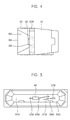
- FIG. 4 is a cross-sectional view of the LED package in FIG. 2 taken along the line of II-II'.
- a protrusion 200 is formed at a longitudinal center of the inner lead 20a receiving the LED chip 40 considering light-emitting efficiency.
- the protrusion 200 may cool heat generated at the LED chip 40 by using external air.
- an opening area is formed wider by the recess 60, so that the light generated at the LED chip 40 emits further without loss of the light.
- a part of the pad frame 20 formed at the substrate 10 may be exposed, and the LED chip 40 may be mounted at the inner lead 20a of the exposed pad frame 20.
- the depth of the recess 60 may be a minimum depth at which the LED chip 40 is buried.
- An inner face of the housing 10b defining the recess 60 is formed to have a predetermined angle at sidewalls to have a wider entrance are of mounting space than a bottom area of the mounting space. Thus, the loss of light may reduced.
- the inner surface of the housing 30 is formed by coating a reflective material or combining a reflection plate having metallic material.
- the reflection plate reflects light emitted from the LED chip 40 and prevents light dispersion.
- the LED package in accordance with an exemplary embodiment includes a zener diode to protect the LED from electrostatic discharge ("ESD").
- the LED package may include a receiving part for receiving the zener diode.
- FIG. 5 is a plan view illustrating an LED package with a voltage regulator diode in accordance with an exemplary embodiment of the present invention.
- the LED package includes a voltage regulator diode.
- the voltage regulator diode may include a zener diode, an aberrancy photo diode (“APD”), etc.
- the voltage regulator diode 270 is mounted at an anode inner lead 250, and an LED 40 is mounted at a cathode inner lead 240.
- the LED 40 may be electrically connected to the anode inner lead 250 over a second wire 220.
- a forward current applied to the anode inner lead 250 is applied to the LED 40 through the second wire 220, so that light is emitted from the LED 40.
- the voltage regulator diode 270 includes a first wire 210.
- the first wire 210 is extended from the voltage regulator diode 270, and is connected to the cathode inner lead 240 by a wire-bonding.
- the first wire 210 is electrically connected to a third wire, which is extended from the LED 40, thereby the voltage regulator diode 270 electrically connected with the LED 40 in parallel.
- a blocking-light dam 260 is disposed between the voltage regulator diode 270 and the LED 40.
- the blocking-light dam blocks the light of the LED 40, and protects the light of the LED 40 from directly irradiating into the voltage regulator diode 270.
- the light-blocking dam 260 may be formed by forming different heights of the substrate 10, which divides areas of the anode inner lead 250 and the cathode inner lead 240.
- the voltage regulator diode 270 is disposed in parallel with the LED 40, so that damages of the LED 40 by the forward and reverse current are preventable.
- the LED device of the side view type is applied.
- the LED device of the present embodiment may be implemented with an LED device of the top view type, a method applying to a flash and a power LED device for lighting.
Landscapes
- Led Device Packages (AREA)
Applications Claiming Priority (1)
| Application Number | Priority Date | Filing Date | Title |
|---|---|---|---|
| KR1020080008519A KR100981214B1 (ko) | 2008-01-28 | 2008-01-28 | 발광다이오드 패키지 |
Publications (1)
| Publication Number | Publication Date |
|---|---|
| EP2083454A2 true EP2083454A2 (fr) | 2009-07-29 |
Family
ID=40592066
Family Applications (1)
| Application Number | Title | Priority Date | Filing Date |
|---|---|---|---|
| EP08005877A Withdrawn EP2083454A2 (fr) | 2008-01-28 | 2008-03-27 | Paquet de diode électroluminescente |
Country Status (5)
| Country | Link |
|---|---|
| US (1) | US7652306B2 (fr) |
| EP (1) | EP2083454A2 (fr) |
| JP (1) | JP2009177187A (fr) |
| KR (1) | KR100981214B1 (fr) |
| TW (1) | TW200933927A (fr) |
Families Citing this family (22)
| Publication number | Priority date | Publication date | Assignee | Title |
|---|---|---|---|---|
| JP5277610B2 (ja) | 2007-10-29 | 2013-08-28 | 日亜化学工業株式会社 | 発光装置及び面発光装置並びに発光装置用パッケージ |
| KR101028852B1 (ko) * | 2008-03-26 | 2011-04-12 | 서울반도체 주식회사 | 사이드뷰 led 패키지 및 이를 포함하는 백라이트 모듈 |
| DE102008049535A1 (de) * | 2008-09-29 | 2010-04-08 | Osram Opto Semiconductors Gmbh | LED-Modul und Herstellungsverfahren |
| TW201128812A (en) | 2009-12-01 | 2011-08-16 | Lg Innotek Co Ltd | Light emitting device |
| KR101034142B1 (ko) * | 2009-12-01 | 2011-05-13 | 엘지이노텍 주식회사 | 발광 소자 및 그 제조방법 |
| JP5734581B2 (ja) * | 2010-05-21 | 2015-06-17 | シャープ株式会社 | 半導体発光装置 |
| US20130043502A1 (en) * | 2010-05-31 | 2013-02-21 | Panasonic Corporation | Light emitting device and method for manufacturing the same |
| KR101049488B1 (ko) * | 2010-06-28 | 2011-07-15 | 주식회사 루멘스 | 측면 발광형 발광소자 패키지 및 백라이트 모듈 |
| US8304797B2 (en) | 2010-07-29 | 2012-11-06 | Osram Sylvania Inc. | Light emitting diode light source having a ceramic substrate |
| KR101078032B1 (ko) | 2010-07-29 | 2011-10-31 | 주식회사 루멘스 | 측면 발광형 발광소자 패키지 및 이를 구비한 백라이트 모듈 |
| JP5537385B2 (ja) * | 2010-11-04 | 2014-07-02 | スタンレー電気株式会社 | サイドビュー型半導体発光装置およびその製造方法 |
| EP2641279B1 (fr) * | 2010-11-19 | 2017-09-27 | Koninklijke Philips N.V. | Porteur de charge îloté pour dispositif électroluminescent |
| US9130109B2 (en) | 2011-01-20 | 2015-09-08 | Rohm Co., Ltd. | Optical apparatus |
| TWI455379B (zh) * | 2011-04-19 | 2014-10-01 | 隆達電子股份有限公司 | 發光二極體封裝結構 |
| CN104752369B (zh) | 2013-12-27 | 2018-02-16 | 展晶科技(深圳)有限公司 | 光电元件模组 |
| JP6142883B2 (ja) * | 2015-02-05 | 2017-06-07 | 日亜化学工業株式会社 | 発光装置 |
| KR102486035B1 (ko) | 2016-01-28 | 2023-01-06 | 쑤저우 레킨 세미컨덕터 컴퍼니 리미티드 | 발광 소자 패키지 및 이를 구비한 발광 장치 |
| JP6842246B2 (ja) * | 2016-05-26 | 2021-03-17 | ローム株式会社 | Ledモジュール |
| TWI626774B (zh) * | 2016-06-13 | 2018-06-11 | 開發晶照明(廈門)有限公司 | Led支架和led封裝結構 |
| JP7257610B2 (ja) * | 2019-07-25 | 2023-04-14 | 日亜化学工業株式会社 | 発光モジュール |
| JP7460911B2 (ja) * | 2020-12-21 | 2024-04-03 | 日亜化学工業株式会社 | 発光装置及びそれを用いたディスプレイ |
| JP7581116B2 (ja) * | 2021-04-22 | 2024-11-12 | スタンレー電気株式会社 | 発光装置及び発光装置の製造方法 |
Family Cites Families (14)
| Publication number | Priority date | Publication date | Assignee | Title |
|---|---|---|---|---|
| JP3673621B2 (ja) * | 1997-07-30 | 2005-07-20 | ローム株式会社 | チップ型発光素子 |
| WO1999007023A1 (fr) * | 1997-07-29 | 1999-02-11 | Osram Opto Semiconductors Gmbh & Co. Ohg | Composant optoelectronique |
| JP3472450B2 (ja) * | 1997-09-04 | 2003-12-02 | シャープ株式会社 | 発光装置 |
| JP4239509B2 (ja) * | 2002-08-02 | 2009-03-18 | 日亜化学工業株式会社 | 発光ダイオード |
| JP2006024794A (ja) * | 2004-07-08 | 2006-01-26 | Sanyo Electric Co Ltd | フルカラー発光ダイオード装置 |
| JP4626258B2 (ja) * | 2004-10-18 | 2011-02-02 | 日亜化学工業株式会社 | 発光ダイオード |
| JP5032747B2 (ja) * | 2005-02-14 | 2012-09-26 | 日亜化学工業株式会社 | 半導体装置 |
| KR100632002B1 (ko) * | 2005-08-02 | 2006-10-09 | 삼성전기주식회사 | 보호 소자를 포함하는 측면형 발광 다이오드 |
| JP4715422B2 (ja) * | 2005-09-27 | 2011-07-06 | 日亜化学工業株式会社 | 発光装置 |
| JP2007142044A (ja) * | 2005-11-16 | 2007-06-07 | Stanley Electric Co Ltd | 半導体発光装置及びそれを用いた面光源 |
| CN100573935C (zh) | 2006-01-25 | 2009-12-23 | 亿光电子工业股份有限公司 | Led封装结构及其制造方法 |
| JP4821343B2 (ja) * | 2006-02-04 | 2011-11-24 | 日亜化学工業株式会社 | サブマウント基板及びこれを備える発光装置 |
| KR100775574B1 (ko) * | 2006-04-20 | 2007-11-15 | 알티전자 주식회사 | 고효율 발광 다이오드 패키지 |
| JP4922663B2 (ja) * | 2006-05-18 | 2012-04-25 | スタンレー電気株式会社 | 半導体光学装置 |
-
2008
- 2008-01-28 KR KR1020080008519A patent/KR100981214B1/ko not_active Expired - Fee Related
- 2008-03-27 EP EP08005877A patent/EP2083454A2/fr not_active Withdrawn
- 2008-03-27 TW TW097110974A patent/TW200933927A/zh unknown
- 2008-03-27 US US12/078,107 patent/US7652306B2/en not_active Expired - Fee Related
-
2009
- 2009-01-27 JP JP2009015723A patent/JP2009177187A/ja active Pending
Also Published As
| Publication number | Publication date |
|---|---|
| TW200933927A (en) | 2009-08-01 |
| JP2009177187A (ja) | 2009-08-06 |
| US20090189174A1 (en) | 2009-07-30 |
| KR20090082641A (ko) | 2009-07-31 |
| US7652306B2 (en) | 2010-01-26 |
| KR100981214B1 (ko) | 2010-09-10 |
Similar Documents
| Publication | Publication Date | Title |
|---|---|---|
| US7652306B2 (en) | Light emitting diode package | |
| US9257624B2 (en) | Light emitting diode package | |
| KR101360732B1 (ko) | 발광 다이오드 패키지 | |
| US10217918B2 (en) | Light-emitting element package | |
| CN102130113B (zh) | 用于半导体发光器件封装的子基板和包括其的半导体发光器件封装 | |
| US8067782B2 (en) | LED package and light source device using same | |
| US20060043407A1 (en) | Semiconductor light emitting apparatus | |
| US20110175512A1 (en) | Light emitting diode and light source module having same | |
| KR20040092512A (ko) | 방열 기능을 갖는 반사판이 구비된 반도체 발광장치 | |
| JP7046796B2 (ja) | 発光装置 | |
| US20110175511A1 (en) | Light emitting diode and light source module having same | |
| CN103545431B (zh) | 发光装置 | |
| US8253159B2 (en) | Semiconductor light emitting device and semiconductor light emitting unit | |
| KR100634189B1 (ko) | 박막형 발광 다이오드 패키지 및 그 제조 방법 | |
| US10355180B2 (en) | Light emitting device and light emitting module | |
| EP3185318B1 (fr) | Dispositif émetteur de lumière et connecteur électrique pour dispositif émetteur de lumière | |
| EP2083453A2 (fr) | Paquet de diode électroluminescente | |
| CN104241262A (zh) | 发光装置以及显示装置 | |
| KR20110108097A (ko) | 발광소자 패키지 및 이를 포함하는 조명시스템 | |
| KR20080087405A (ko) | Led 패키지 및 그 제조방법 | |
| KR20120019697A (ko) | 발광소자 패키지 및 이를 채용한 멀티칩 조명모듈 | |
| KR20110115320A (ko) | 발광소자 패키지, 그 제조방법 및 조명시스템 |
Legal Events
| Date | Code | Title | Description |
|---|---|---|---|
| PUAI | Public reference made under article 153(3) epc to a published international application that has entered the european phase |
Free format text: ORIGINAL CODE: 0009012 |
|
| 17P | Request for examination filed |
Effective date: 20080327 |
|
| AK | Designated contracting states |
Kind code of ref document: A2 Designated state(s): AT BE BG CH CY CZ DE DK EE ES FI FR GB GR HR HU IE IS IT LI LT LU LV MC MT NL NO PL PT RO SE SI SK TR |
|
| AX | Request for extension of the european patent |
Extension state: AL BA MK RS |
|
| RIN1 | Information on inventor provided before grant (corrected) |
Inventor name: KIM, SUN-HONG Inventor name: PARK, KYOUNG-IL Inventor name: LEE, JIN WON |
|
| STAA | Information on the status of an ep patent application or granted ep patent |
Free format text: STATUS: THE APPLICATION HAS BEEN WITHDRAWN |
|
| 18W | Application withdrawn |
Effective date: 20130911 |