EP2085812A2 - Filmfilter für einen Flachbildschirm - Google Patents
Filmfilter für einen Flachbildschirm Download PDFInfo
- Publication number
- EP2085812A2 EP2085812A2 EP08172821A EP08172821A EP2085812A2 EP 2085812 A2 EP2085812 A2 EP 2085812A2 EP 08172821 A EP08172821 A EP 08172821A EP 08172821 A EP08172821 A EP 08172821A EP 2085812 A2 EP2085812 A2 EP 2085812A2
- Authority
- EP
- European Patent Office
- Prior art keywords
- layer
- film filter
- filter according
- disposed
- electrode layer
- Prior art date
- Legal status (The legal status is an assumption and is not a legal conclusion. Google has not performed a legal analysis and makes no representation as to the accuracy of the status listed.)
- Withdrawn
Links
Images

Classifications
-
- G—PHYSICS
- G02—OPTICS
- G02B—OPTICAL ELEMENTS, SYSTEMS OR APPARATUS
- G02B5/00—Optical elements other than lenses
- G02B5/20—Filters
-
- H—ELECTRICITY
- H01—ELECTRIC ELEMENTS
- H01J—ELECTRIC DISCHARGE TUBES OR DISCHARGE LAMPS
- H01J11/00—Gas-filled discharge tubes with alternating current induction of the discharge, e.g. alternating current plasma display panels [AC-PDP]; Gas-filled discharge tubes without any main electrode inside the vessel; Gas-filled discharge tubes with at least one main electrode outside the vessel
- H01J11/10—AC-PDPs with at least one main electrode being out of contact with the plasma
- H01J11/12—AC-PDPs with at least one main electrode being out of contact with the plasma with main electrodes provided on both sides of the discharge space
-
- G—PHYSICS
- G02—OPTICS
- G02B—OPTICAL ELEMENTS, SYSTEMS OR APPARATUS
- G02B5/00—Optical elements other than lenses
- G02B5/20—Filters
- G02B5/208—Filters for use with infrared or ultraviolet radiation, e.g. for separating visible light from infrared and/or ultraviolet radiation
-
- G—PHYSICS
- G02—OPTICS
- G02B—OPTICAL ELEMENTS, SYSTEMS OR APPARATUS
- G02B5/00—Optical elements other than lenses
- G02B5/20—Filters
- G02B5/22—Absorbing filters
- G02B5/223—Absorbing filters containing organic substances, e.g. dyes, inks or pigments
-
- G—PHYSICS
- G02—OPTICS
- G02F—OPTICAL DEVICES OR ARRANGEMENTS FOR THE CONTROL OF LIGHT BY MODIFICATION OF THE OPTICAL PROPERTIES OF THE MEDIA OF THE ELEMENTS INVOLVED THEREIN; NON-LINEAR OPTICS; FREQUENCY-CHANGING OF LIGHT; OPTICAL LOGIC ELEMENTS; OPTICAL ANALOGUE/DIGITAL CONVERTERS
- G02F1/00—Devices or arrangements for the control of the intensity, colour, phase, polarisation or direction of light arriving from an independent light source, e.g. switching, gating or modulating; Non-linear optics
- G02F1/01—Devices or arrangements for the control of the intensity, colour, phase, polarisation or direction of light arriving from an independent light source, e.g. switching, gating or modulating; Non-linear optics for the control of the intensity, phase, polarisation or colour
- G02F1/13—Devices or arrangements for the control of the intensity, colour, phase, polarisation or direction of light arriving from an independent light source, e.g. switching, gating or modulating; Non-linear optics for the control of the intensity, phase, polarisation or colour based on liquid crystals, e.g. single liquid crystal display cells
- G02F1/133—Constructional arrangements; Operation of liquid crystal cells; Circuit arrangements
- G02F1/1333—Constructional arrangements; Manufacturing methods
- G02F1/1347—Arrangement of liquid crystal layers or cells in which the final condition of one light beam is achieved by the addition of the effects of two or more layers or cells
-
- H—ELECTRICITY
- H01—ELECTRIC ELEMENTS
- H01J—ELECTRIC DISCHARGE TUBES OR DISCHARGE LAMPS
- H01J11/00—Gas-filled discharge tubes with alternating current induction of the discharge, e.g. alternating current plasma display panels [AC-PDP]; Gas-filled discharge tubes without any main electrode inside the vessel; Gas-filled discharge tubes with at least one main electrode outside the vessel
- H01J11/20—Constructional details
- H01J11/34—Vessels, containers or parts thereof, e.g. substrates
- H01J11/44—Optical arrangements or shielding arrangements, e.g. filters, black matrices, light reflecting means or electromagnetic shielding means
-
- H—ELECTRICITY
- H01—ELECTRIC ELEMENTS
- H01J—ELECTRIC DISCHARGE TUBES OR DISCHARGE LAMPS
- H01J5/00—Details relating to vessels or to leading-in conductors common to two or more basic types of discharge tubes or lamps
- H01J5/02—Vessels; Containers; Shields associated therewith; Vacuum locks
-
- H—ELECTRICITY
- H05—ELECTRIC TECHNIQUES NOT OTHERWISE PROVIDED FOR
- H05K—PRINTED CIRCUITS; CASINGS OR CONSTRUCTIONAL DETAILS OF ELECTRIC APPARATUS; MANUFACTURE OF ASSEMBLAGES OF ELECTRICAL COMPONENTS
- H05K9/00—Screening of apparatus or components against electric or magnetic fields
-
- H—ELECTRICITY
- H01—ELECTRIC ELEMENTS
- H01J—ELECTRIC DISCHARGE TUBES OR DISCHARGE LAMPS
- H01J2211/00—Plasma display panels with alternate current induction of the discharge, e.g. AC-PDPs
- H01J2211/20—Constructional details
- H01J2211/34—Vessels, containers or parts thereof, e.g. substrates
- H01J2211/44—Optical arrangements or shielding arrangements, e.g. filters or lenses
- H01J2211/444—Means for improving contrast or colour purity, e.g. black matrix or light shielding means
Definitions
- the present invention relates to a film filter and a flat panel display having the same capable of increasing brightness and improving bright room contrast ratio.
- a plasma display panel is a flat panel display using a gas discharge (plasma) phenomenon.
- Plasma display panels may be one of the next generation displays since they can simultaneously be large and thin compared to a CRT.
- the plasma display panel is driven by discharge to emit electromagnetic interference, the electromagnetic waves affecting a human body or other electronic equipment. Therefore, the existing plasma display panel is requested to lower the emitted electromagnetic interference below a permissible level. To this end, most of the existing plasma display panels adopt a front filter capable of improving bright room contrast ratio by lowering reflectivity of external light simultaneously with blocking electromagnetic interference and near infrared rays.
- the front filter is divided into a reinforced glass filter and a film filter according to use or non-use of glass.
- the reinforced glass filter is advantageous in that it is strong against external impact.
- the reinforced glass filter is disadvantageous in that it is heavy and expensive in installation since it has a thickness of about 3mm.
- the film filter is advantageous in that it is light and thin and improves a duplicated image.
- the film filter has the same transmissivity of internal light as external light in view of light efficiency so that it has limitations in improving visibility and bright room/dark room contrast ratio of the display.
- the front filter has a light transmissivity of about 40 to 55% due to a colorant, etc. absorbing light of a specific wavelength in order to improve light properties, but such a light transmissivity lowers brightness of the display to cause a problem of bad visibility. Meanwhile, if the light transmissivity of the front filter is designed to be higher than 55%, the brightness is raised, but the bright room contrast ratio is reduced due to strong external light scattering. Accordingly, it is difficult to implement a high-quality moving picture.
- the present embodiments overcome the above problems as well as provide additional advantages.
- a film filter that is directly attached on a visible surface of a display, the film filter comprising: a support layer formed with a plurality of holes; first and second electrode layers disposed on both sides of the support layer; and a blind member inserted into the holes and of which transmittance is changed depending on an electric field applied through the first and second electrode layers.
- the blind member may be formed of at least any one of suspended particles, photochromic devices, electrochromic devices, etc.
- the film filter may further include an upper layer formed of an anti-reflective coating layer and/or an anti-glare layer.
- the film filter may further include an upper layer for any one of color correction, neon light block, and near infrared ray block.
- the film filter may further include an electromagnetic interference shielding layer as an upper layer.
- the upper means an opposite side thereto.
- the film filter may further include an adhesion layer.
- the adhesion layer may include a colorant for any one of color correction, neon light blocking, and near infrared ray blocking.
- the film filter may further include a transparent film.
- the transparent film may support the upper layer or the electromagnetic interference shielding layer.
- the film filter may further include a power supply unit applying voltage between the first electrode layer and the second electrode layer.
- a flat panel display comprising: a flat panel display body; and a film filter attached on a visible surface of the flat panel display body, wherein the film filter is the film filter according to one aspect of the present embodiments.
- a support layer of the film filter has a black-based color, and has a pattern structure corresponding to a non-light-emitting region among a light-emitting region and the non-light-emitting region of the flat panel display.
- transparent means being both substantially transparent as well as having transmissivity to the extent that it is commonly considered as transparent in this technical field.
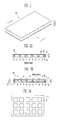
- FIG. 1 is a perspective view of a film filter according to one embodiment.
- a film filter 10 comprises a first electrode layer 11 and a second electrode layer 12 disposed to be opposed to each other, and a support layer 13 disposed between the first electrode 11 and the second electrode layer 12.
- the film filter 10 may be attached on a visible surface of the flat panel display, using for example an adhesion layer.
- the support layer 13 of the film filter 10 is patterned to have a light transmitting region and light non-transmitting region, wherein the light transmitting region includes a blind member, the transmittance of which can be changed depending on the applied electric field.
- FIG. 2a and FIG. 2b are cross-sectional views explaining a structure and an operation process of a film filter of the present embodiments.
- FIG. 2a and FIG. 2b are cross-sections of the film filter taken along line I-I' of FIG. 1 .
- a support 13 is disposed between a first electrode layer 11 and a second electrode layer 12 of a film filter 10 and has a penetrating hole 14, also referred to as a through hole, or just hole.
- the support layer 13 may has a lattice shape by means of the penetrating hole 14. (See FIG.
- the support layer 13 may be made, for example, of at least one material selected from the group consisting of polyethersulphone (PES), polyacrylate (PAR), polyetherimide (PEI), polyethylene napthalate (PEN), polyethylene terephthalate (PET), polyphenylene sulfide (PPS), polyallylate, polyimide, polycabonate, triacetate cellulose (TAC), and cellulose acetate propionate (CAP).
- PES polyethersulphone
- PAR polyacrylate
- PEI polyetherimide
- PEN polyethylene napthalate
- PET polyethylene terephthalate
- PPS polyphenylene sulfide
- polyallylate polyimide
- TAC triacetate cellulose
- CAP cellulose acetate propionate
- the support layer 13 includes a black-based colorant 15 in order to block the transmission of internal light and to absorb external light.
- the colorant may include material capable of representing the support layer 13 in, for example, black, e.g., a general pigment or dye capable of absorbing light of desired wavelength in a visible region, wherein the sort thereof is not specially limited.
- the colorant can include organic colorants, such as an anthraquinone-based organic colorant, a phthalocyanine-based organic colorant, a methine-based organic colorant, an azomethine-based organic colorant, an oxadine-based organic colorant, an azo-based organic colorant, a styryl-based organic colorant, a coumarin-based organic colorant, a porphyrin-based organic colorant, a dibenzofuran -based organic colorant, a diketo-pyrrolo-pyrrole-based organic colorant, a rhodamine-based organic colorant, a xanthene-based organic colorant, and a pyrromethene-based organic colorant.
- organic colorants such as an anthraquinone-based organic colorant, a phthalocyanine-based organic colorant, a methine-based organic colorant, an azomethine-based organic colorant, an
- the support layer 13 is formed of a black layer patterned in an approximate lattice shape.
- the first electrode layer 11 and/or the second electrode layer 12 may be made of transparent material.
- the transparent material may include indium tin oxide (ITO), SnO2, etc.
- ITO indium tin oxide
- SnO2 SnO2
- the first electrode layer 11 and/or the second electrode layer 12 may perform the function of shielding electromagnetic interference (EMI) emitted to a screen of a flat panel display.
- EMI shielding electromagnetic interference
- Black, black-base or black-based color mean colors capable of blocking or absorbing most of the incident light as well as color commonly having a low transmissivity below a predetermined value in this technical field.
- a blind member 16 is disposed on the penetrating hole 14 of the support layer 13.
- the transmittance of the blind member 16 is changed depending on the electric field applied through the first electrode layer 11 and the second electrode layer 12. For example, the blind member 16 becomes transparent to transmit light when the electric field is applied, and the blind member 16 becomes opaque to block light when the electric field is not applied.
- the blind member 16 may comprise, for example, suspended particles, photochromic devices, electrochromic devices, etc.
- the blind member is also referred to herein as a variable transmittance element.
- liquid crystal molecules, that are suspended particles, of the blind member 16 which is manufactured by mixing liquid crystal molecules with polymers exhibit random Brownian motion when the electric field is not applied, the incident light is absorbed or scattered to show a low transmittance.
- the liquid crystal molecules are arranged in the electric field direction to be a transparent state, exhibiting high transmittance.
- the blind member 16 using the suspended particles has additional advantages, beingcapable of blocking ultraviolet rays of about 99% or more and reflecting near infrared rays, in addition to advantages of being capable of easily controlling transmittance as a result of application of the electric field to the first electrode layer 11 and the second electrode layer 12.
- the film filter 10 substantially does not transmit internal light to the outside through the support layer 13 and the blind member 16 in a standby mode, e.g.., in a mode where voltage is not applied to a first conductive layer 11 and a second conductive layer 12, as shown in FIG. 2a .
- the film filter 10 When voltage is applied to the first conductive layer 11 and the second conductive layer 12 from a power supply unit 17, as shown in FIG. 2b , the film filter 10 is converted to an active mode from the standby mode. At this time, the transmittance of the blind member 16 is changed to transmit the internal light to the outside.
- the external light may be absorbed by a black support layer 13.
- An alternating voltage (AC) of from about 30 to about 100V is required in the case of the blind member 16 using the suspended particles.
- the bright room/dark room contrast ration of the flat panel display can be improved through a light transmitting region of the blind member 16 corresponding to the pattern structure of the pixels and a light non-transmitting region of the support layer 13 corresponding to the non-light-emitting region when operating the flat panel display.
- brightness of the flat panel display is set to be high, desired bright room contrast ratio and visibility of the flat panel display can be easily secured through the light transmitting region of the blind member 16 and the light non-transmitting region of the support layer 13.
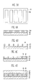
- FIG. 3a and FIG. 3b are plan views of a structure of a support layer adoptable to a film filter of the present embodiments.
- a support layer 13 may have a pattern structure in a lattice shape having a plurality of penetrating holes 14 separately arranged at predetermined intervals in view of a plan.
- the shapes of the penetrating holes 14 are identically shown as a square or rectangle, each shape thereof may be identically or individually designed to be a polygon, a circle or a polygon including a circular arc, etc. by corresponding to each pixel region corresponding to each light-emitting region of the flat panel display on which the film filter is to be installed.
- the shape of the support layer 13 may be designed to have a stripe shape where the penetrating hole 14a is extended in one direction (up and down direction in FIG. 4 ), by corresponding to a pixel region of the flat panel display in one direction on which the film filter is to be installed.
- FIG. 4a to FIG. 4e are cross-sectional views showing a manufacturing process of a film filter of the present embodiments.
- PET polyethylene terephthalate
- a black PET film 23A including a colorant is prepared through a similar process with the preparation process of the PET film 21. For example, when manufacturing the PET film, it is melted and compressed by adding a predetermined content of black-based colorant with the PET pellets, making it possible to make a black PET film.
- a conductive film 22 is formed on the transparent PET film 21.
- the conductive film 22 corresponds to the first electrode layer or the second electrode layer.
- the black PET film 23A is attached on the conductive film 22. The attachment may be performed through a roll to roll process.
- the black PET film 23A is patterned through a laser etching process to form a penetrating hole 24 so that a support layer 23 having a desired pattern structure is formed.
- a blind member 25 is inserted into the penetrating hole 24 through, for example, a screen printing method, an inkjet printing method, a deposition method, etc.
- laminate formed with another conductive film 26 on another transparent PET film 27 is attached on the support layer 23 and the blind member 25 to manufacture a film filter.
- the conductive films 22 and 26 may have a pattern structure including a main pattern corresponding to a penetrating hole 24 pattern (Refer to 14 of FIG. 3a ) and a bus pattern (not shown) electrically coupling the main pattern and being exposed to the exterior.
- a pair of conductive films 22 and 26 may have a pattern structure where they are faced symmetrically putting the support layer 23 therebetween.
- Such a structure may be formed through a process such as a photolithography progress.
- the layers 21, 23 and 27 made of the same PET material contact each other so that they can be easily attached to each other at high strength under a predetermined pressure and atmosphere.
- the conductive layers 22 and 26 of the present embodiment may be formed by being applied to almost entire surfaces of the transparent films 21 and 27, respectively.
- the present embodiments allow the support layer 23 to be directly contacted to the transparent films 21 and 27 by removing at least a portion of edges of the conductive films 22 and 26, making it possible to improve adhesion strength between the respective layers of the film filter.
- the manufacturing method of the film filter of the present embodiment may use a method that inserts the blind member 25 into the penetrating hole 24 through a small gap coupling the external to the penetrating hole 24, in a state where the transparent films 21 and 27 attached with the conductive films 22 and 26 are stacked on both sides of the support layer 23 having the penetrating hole 24, and then blocks the gap.
- the blind member 25 is inserted into the penetrating hole 24, for example, by means of a capillary phenomenon or an atmospheric pressure difference.
- FIG. 5 is a cross-sectional view of a film filter according to another embodiment.
- a film filter of the present embodiments may additionally include at least one functional layer A, B, and C, in addition to a basic filter structure.
- the basic filter structure means the film filter 10 previously described with reference to FIG. 2a , and it will be referred to as a base layer 10 in the following description.
- the film filter includes a first transparent film 32a disposed on one surface (hereinafter, referred to as a lower surface) of the base layer 10.
- the first transparent film 32a corresponds to the transparent film 21 of FIG. 4d .
- a first adhesion layer 30a is disposed on the first transparent film 32a.
- the first adhesion layer 30a may be used when directly attaching the film filter to a visible surface of a flat panel display.
- the film filter includes a second transparent film 32b disposed on the other surface (hereinafter, referred to as an upper surface) of the base layer 10.
- the second transparent film 32b corresponds to the transparent film 27 of FIG. 4d .
- An electromagnetic interference (EMI) shielding layer 34 that blocks electromagnetic interference is disposed on the second transparent film 32b.
- the electromagnetic interference (EMI) shielding layer 34 may be installed as a copper (Cu) thin film in a mesh shape or a conductive film having another predetermined pattern.
- a third transparent film 32c is disposed on the electromagnetic interference (EMI) shielding layer 34 by interposing a second adhesion layer 30b.
- the second adhesion layer 30b and the third transparent film 32c are installed in order to support an upper layer to be installed thereon, to improve adhesion strength between the upper layer and the electromagnetic (EMI) shielding layer 34 and to planarize the interface therebetween.
- a color coating layer 36 for any color correction is disposed on the third transparent film 32c.
- the color coating layer 36 includes a colorant such as a pigment or dye capable of selectively absorbing light of a specific wavelength in a visible light region.
- the colorant may comprise compounds capable of blocking unnecessary light with a wavelength of about 585nm emitted when neon is excited, such as, for example, a cyanine-based compound, an azomethine-based compound, a xanthene-based compound, an oxonol-based compound, an azo-based compound, etc.
- a fourth transparent film 32d is disposed on the color coating layer 36 by interposing a third adhesion layer 30c.
- the third adhesion layer 30c and the fourth transparent film 32d are installed to support an upper layer to be installed thereon, to improve adhesion strength between the upper layer and the color coating layer 36 and to planarize the interface therebetween.
- the color coating layer 36 and the third transparent film 32c and the third adhesion layer 30c disposed on the upper and lower surfaces of the color coating layer 36 may be omitted.
- the anti-reflective coating layer 38 that prevents reflection and/or glare is formed on the fourth transparent film 32d.
- the anti-reflective coating layer 38 is disposed in order to minimize loss of the transmitted light and to prevent reflection and diffused reflection of external light.
- the anti-reflective coating layer 38 may be installed in a single layer structure or a multi-layer structure, wherein the single layer structure includes a thin film of fluorine-based transparent polymer resin, fluorinated magnesium, silicon-based resin, silicon oxide, etc., which has an optical film thickness of 1/4 wavelength, and the multi-layer structure includes inorganic compounds such as metal oxide, fluoride, silicide, carbide, nitride, and sulfide, which have different refraction indexes, and organic compounds such as silicon-based resin, acrylic resin, or fluoride-based resin, etc., in two or more layers.
- a sputtering method When forming the anti-reflective coating layer 38, a sputtering method, an ion plating method, an ion beam assist method, a vacuum deposition method, a chemical vapor deposition (CVD) method, a physical vapor deposition (PVD) method, etc. may be used.
- a vacuum deposition method When forming the anti-reflective coating layer 38, a sputtering method, an ion plating method, an ion beam assist method, a vacuum deposition method, a chemical vapor deposition (CVD) method, a physical vapor deposition (PVD) method, etc.
- CVD chemical vapor deposition
- PVD physical vapor deposition
- the film filter of the present embodiments may further include hard coating materials disposed on the anti-reflective coating layer 38.
- the hard coating materials may be installed for preventing scratch due to various forms of external force. It may be made using, for example, acrylic-based polymer, urethane-based polymer, epoxy-based polymer, siloxane-based polymer and it may be also made using ultraviolet rays reinforced resin such as an oligomer. In order to improve strength, silica-based filler may be additionally included.
- the aforementioned hard coating materials may be inserted into the anti-reflective coating layer 38, or may be disposed on the lower surface of the anti-reflective coating layer 38, e.g.., between the anti-reflective coating layer 38 and the fourth transparent film 32d, or may be disposed on the upper surface of the anti-reflective coating layer 38.
- the anti-reflective coating layer 38 including the hard coating material has a thickness T of from about 2 to about 7 ⁇ m not to make its thickness too thick and to obtain the expected effects, wherein the anti-reflective coating layer 38 is exemplary designed to have the optical characteristics such as a low haze of from about 1 to about 3%, a visible transmittance of from about 30% to about 90%, a low external light reflectivity of from about 1 to about 20%, heat resistance of a glass transition temperature or more, and a pencil hardness of from about 2 to about 3H.
- FIG. 6 is a cross-sectional view of a flat panel display that comprises a film filter of the present embodiments.
- a plasma display panel will be described as a flat panel display by way of example.
- a plasma display panel includes a panel body 50 and a film filter 10 attached to a visible surface of the panel body 50.
- the film filter 10 is the film filter explained above with reference to FIG. 2a .
- the film filter 10 may be replaced by another film filter explained above with reference to FIG. 5 .
- the panel body 50 includes a front plate and a back plate disposed to be opposed to each other.
- the front plate includes a first substrate 51, X-Y electrodes (not shown) disposed on the first substrate 51, a first dielectric layer 52 and a protecting layer (not shown), and the back plate includes a second substrate 53, an address electrode disposed on the second substrate 53, a second dielectric layer 54, a barrier rib 55, and a phosphor layer 56.
- the panel body 50 includes a chassis base supporting a coupling structure of the front plate and the back plate and a driving circuit board disposed on one surface of the chassis base and configured of circuits driving the panel. The detailed structure and the operation principle of the panel body 50 will be omitted.
- a penetrating hole 14 of a support layer 13 filled with a blind member 16 of a film filter 10 is disposed to face a discharge cell region of the panel body 50, that is, a discharge space where the phosphor 56 is applied, and a support layer 13 is disposed to face the barrier rib 55.
- a penetrating hole 14 of a support layer 13 filled with a blind member 16 of a film filter 10 is disposed to face a discharge cell region of the panel body 50, that is, a discharge space where the phosphor 56 is applied, and a support layer 13 is disposed to face the barrier rib 55.
- a power supply unit applying voltage to a first electrode layer 11 and a second electrode layer 12 of the film filter 10 may be included in a driving circuit or a power supply device mounted on the driving circuit board 57 within the panel body 50.
- the film filter can be operated depending on the operation or non-operation of the driving circuit, making it possible to easily control the film filter 10.
- a separate power supply unit for operating the film filter 10 may be omitted so that it is economic.
- the plasma display panel is described as an illustrative example of a flat panel display.
- the present embodiments are not limited thereto.
- the present embodiments can be applied to display apparatuses such as a field emission display (FED), a vacuum fluorescent display (VFD), an organic light emitting display (OLED), a liquid crystal display (LCD), etc.
- FED field emission display
- VFD vacuum fluorescent display
- OLED organic light emitting display
- LCD liquid crystal display
- the film filter of the present embodiments can remarkably improve bright room/dark room contrast ratio and visibility of the flat panel display by means of the black support layer acting on the light non-transmitting region and the blind member acting on the light transmitting region when an electric field is applied.
- the present embodiments can obtain the effect of the film filter compared with the reinforced glass filter, for example, the effect of removing a duplicated image due to the removal of interface with the flat panel display, and the effects making the flat panel display lightweight, thin and inexpensive.
Landscapes
- Physics & Mathematics (AREA)
- General Physics & Mathematics (AREA)
- Optics & Photonics (AREA)
- Engineering & Computer Science (AREA)
- Plasma & Fusion (AREA)
- Nonlinear Science (AREA)
- Electromagnetism (AREA)
- Toxicology (AREA)
- Health & Medical Sciences (AREA)
- Crystallography & Structural Chemistry (AREA)
- Chemical & Material Sciences (AREA)
- Mathematical Physics (AREA)
- Microelectronics & Electronic Packaging (AREA)
- Devices For Indicating Variable Information By Combining Individual Elements (AREA)
- Optical Filters (AREA)
- Liquid Crystal (AREA)
- Surface Treatment Of Optical Elements (AREA)
- Control Of Indicators Other Than Cathode Ray Tubes (AREA)
- Control Of Gas Discharge Display Tubes (AREA)
Applications Claiming Priority (1)
| Application Number | Priority Date | Filing Date | Title |
|---|---|---|---|
| KR1020080009045A KR100941844B1 (ko) | 2008-01-29 | 2008-01-29 | 필름 필터 및 이를 구비하는 평판 표시장치 |
Publications (1)
| Publication Number | Publication Date |
|---|---|
| EP2085812A2 true EP2085812A2 (de) | 2009-08-05 |
Family
ID=40751229
Family Applications (1)
| Application Number | Title | Priority Date | Filing Date |
|---|---|---|---|
| EP08172821A Withdrawn EP2085812A2 (de) | 2008-01-29 | 2008-12-23 | Filmfilter für einen Flachbildschirm |
Country Status (5)
| Country | Link |
|---|---|
| US (1) | US20090190198A1 (de) |
| EP (1) | EP2085812A2 (de) |
| JP (1) | JP2009181118A (de) |
| KR (1) | KR100941844B1 (de) |
| CN (1) | CN101498801A (de) |
Cited By (2)
| Publication number | Priority date | Publication date | Assignee | Title |
|---|---|---|---|---|
| EP2110842A3 (de) * | 2008-04-14 | 2010-07-28 | Samsung SDI Co., Ltd. | Folieneinheit und Plasmaanzeigetafel mit dieser |
| EP2463705A1 (de) * | 2010-12-13 | 2012-06-13 | Samsung Corning Precision Materials Co., Ltd. | Flachbildschirm und Herstellungsverfahren dafür |
Families Citing this family (19)
| Publication number | Priority date | Publication date | Assignee | Title |
|---|---|---|---|---|
| JP5328159B2 (ja) | 2005-03-01 | 2013-10-30 | セルカコア・ラボラトリーズ・インコーポレーテッド | 多波長センサ発光体 |
| KR20090125416A (ko) * | 2008-06-02 | 2009-12-07 | 삼성에스디아이 주식회사 | 광학 필터 및 그를 구비하는 플라즈마 표시 장치 |
| US20100004518A1 (en) | 2008-07-03 | 2010-01-07 | Masimo Laboratories, Inc. | Heat sink for noninvasive medical sensor |
| US8630691B2 (en) | 2008-08-04 | 2014-01-14 | Cercacor Laboratories, Inc. | Multi-stream sensor front ends for noninvasive measurement of blood constituents |
| CN102737576B (zh) * | 2011-04-12 | 2014-12-10 | 神基科技股份有限公司 | 透明显示装置及其操作方法 |
| US20140333991A1 (en) * | 2012-01-19 | 2014-11-13 | Sharp Kabushiki Kaisha | Display panel and display device |
| KR101448671B1 (ko) * | 2012-12-07 | 2014-10-13 | 주식회사 엔케이이씨 | 전기 변색 필름 및 이의 제조방법 |
| KR101448673B1 (ko) * | 2012-12-07 | 2014-10-08 | 주식회사 엔케이이씨 | 전기 변색 필름 및 이의 제조방법 |
| CN104216191B (zh) * | 2013-05-31 | 2017-05-10 | 赛恩倍吉科技顾问(深圳)有限公司 | 电致变色膜 |
| CN103529615B (zh) * | 2013-11-06 | 2016-04-20 | 京东方科技集团股份有限公司 | 显示面板及其制造方法、显示装置 |
| JP6597373B2 (ja) | 2015-06-19 | 2019-10-30 | 株式会社リコー | エレクトロクロミック素子、表示装置及びその駆動方法 |
| EP3265872B1 (de) * | 2015-07-08 | 2020-07-01 | Hewlett-Packard Development Company, L.P. | Elektrophoretische datenschutzvorrichtungen |
| KR102568924B1 (ko) | 2016-06-14 | 2023-08-22 | 삼성디스플레이 주식회사 | 표시 장치 및 이를 포함하는 룸미러 모듈 |
| DE102016111159A1 (de) * | 2016-06-17 | 2017-12-21 | Visteon Global Technologies, Inc. | Displayanordnung und Verfahren zur Anzeige von Informationen |
| KR101982386B1 (ko) | 2016-10-31 | 2019-05-27 | 삼성에스디아이 주식회사 | 편광판 및 이를 포함하는 액정표시장치 |
| CN110456548B (zh) * | 2019-08-30 | 2022-04-26 | 京东方科技集团股份有限公司 | 调光结构及其制备方法 |
| KR20220129033A (ko) | 2020-01-13 | 2022-09-22 | 마시모 코오퍼레이션 | 생리학적 파라미터 모니터링 기능이 있는 웨어러블 디바이스 |
| CN112242098B (zh) * | 2020-10-14 | 2022-08-05 | Tcl华星光电技术有限公司 | 基板及其制备方法、显示面板 |
| EP4370022A1 (de) | 2021-07-13 | 2024-05-22 | Masimo Corporation | Tragbare vorrichtung mit überwachung physiologischer parameter |
Family Cites Families (15)
| Publication number | Priority date | Publication date | Assignee | Title |
|---|---|---|---|---|
| US4919521A (en) * | 1987-06-03 | 1990-04-24 | Nippon Sheet Glass Co., Ltd. | Electromagnetic device |
| JPH087391Y2 (ja) * | 1990-03-09 | 1996-03-04 | トヨタ自動車株式会社 | 粒子分散型表示素子 |
| JPH05263572A (ja) * | 1992-03-19 | 1993-10-12 | Idemitsu Kosan Co Ltd | フレキシブルブラインド |
| WO1998013850A1 (en) * | 1996-09-26 | 1998-04-02 | Asahi Glass Company Ltd. | Plasma display protective plate and its manufacturing method |
| JP2006058896A (ja) * | 2000-02-01 | 2006-03-02 | Mitsui Chemicals Inc | プラズマディスプレイ用フィルタ、表示装置およびその製造方法 |
| JP2004354740A (ja) * | 2003-05-29 | 2004-12-16 | Fuji Photo Film Co Ltd | 反射防止膜、反射防止フィルムおよび画像表示装置 |
| JP2005157081A (ja) * | 2003-11-27 | 2005-06-16 | Fujitsu Hitachi Plasma Display Ltd | プラズマディスプレイ装置 |
| KR100531796B1 (ko) * | 2003-12-10 | 2005-12-02 | 엘지전자 주식회사 | 플라즈마 디스플레이 패널용 광셔터 및 그 구동방법 |
| JP2005181933A (ja) * | 2003-12-24 | 2005-07-07 | Nisshinbo Ind Inc | 光学フィルター |
| JP4604484B2 (ja) * | 2003-12-25 | 2011-01-05 | 富士ゼロックス株式会社 | 光学素子 |
| WO2006015044A1 (en) * | 2004-07-27 | 2006-02-09 | E Ink Corporation | Electro-optic displays |
| TWI306533B (en) * | 2005-03-15 | 2009-02-21 | Ind Tech Res Inst | A transflective electrophoresis display and manufacturing method |
| JP2007264628A (ja) * | 2006-03-28 | 2007-10-11 | Samsung Sdi Co Ltd | フィルタ、それを備えたディスプレイ装置及びその製造方法 |
| KR20070111834A (ko) * | 2006-05-19 | 2007-11-22 | 엘지전자 주식회사 | 플라즈마 디스플레이 패널의 전면필터 |
| WO2007148721A1 (ja) * | 2006-06-22 | 2007-12-27 | Pioneer Corporation | 表示装置及び光学フィルタ |
-
2008
- 2008-01-29 KR KR1020080009045A patent/KR100941844B1/ko not_active Expired - Fee Related
- 2008-05-14 JP JP2008126813A patent/JP2009181118A/ja active Pending
- 2008-11-07 US US12/291,278 patent/US20090190198A1/en not_active Abandoned
- 2008-11-27 CN CNA2008101815733A patent/CN101498801A/zh active Pending
- 2008-12-23 EP EP08172821A patent/EP2085812A2/de not_active Withdrawn
Cited By (4)
| Publication number | Priority date | Publication date | Assignee | Title |
|---|---|---|---|---|
| EP2110842A3 (de) * | 2008-04-14 | 2010-07-28 | Samsung SDI Co., Ltd. | Folieneinheit und Plasmaanzeigetafel mit dieser |
| US8227986B2 (en) | 2008-04-14 | 2012-07-24 | Samsung Sdi Co., Ltd. | Film unit and plasma display panel having the same |
| EP2463705A1 (de) * | 2010-12-13 | 2012-06-13 | Samsung Corning Precision Materials Co., Ltd. | Flachbildschirm und Herstellungsverfahren dafür |
| US8598772B2 (en) | 2010-12-13 | 2013-12-03 | Samsung Corning Precision Materials Co., Ltd. | Flat display and method of fabricating the same |
Also Published As
| Publication number | Publication date |
|---|---|
| KR20090083086A (ko) | 2009-08-03 |
| KR100941844B1 (ko) | 2010-02-11 |
| JP2009181118A (ja) | 2009-08-13 |
| CN101498801A (zh) | 2009-08-05 |
| US20090190198A1 (en) | 2009-07-30 |
Similar Documents
| Publication | Publication Date | Title |
|---|---|---|
| EP2085812A2 (de) | Filmfilter für einen Flachbildschirm | |
| JP4739951B2 (ja) | ディスプレイ装置用フィルター及びこれを含んだディスプレイ装置 | |
| KR101066546B1 (ko) | 그라데이션 장식구조를 갖는 디스플레이 필터 및 보호 케이스 | |
| KR20090021009A (ko) | 디스플레이 장치용 전자파 차폐 부재 | |
| KR101043692B1 (ko) | 디스플레이 장치용 필터 및 이를 포함한 디스플레이 장치 | |
| US20100079049A1 (en) | Plasma display device | |
| KR20090021693A (ko) | 광학필름, 그 제조방법 및 이를 포함하는 표시장치 | |
| KR100615338B1 (ko) | 플라즈마 디스플레이 장치 | |
| KR20090125416A (ko) | 광학 필터 및 그를 구비하는 플라즈마 표시 장치 | |
| MX2007009089A (es) | Capa protectora contra la luz externa y aparato de visualización que la contiene. | |
| CN100504455C (zh) | 外界光屏蔽层、用于包括外界光屏蔽层的显示装置的滤光器以及包括滤光器的显示装置 | |
| KR20090065094A (ko) | 디스플레이 장치용 광학 부재 및 이를 포함하는 디스플레이장치용 필터 | |
| EP2192429A1 (de) | Optischer Filter für Anzeigevorrichtungen | |
| KR101049460B1 (ko) | 디스플레이 장치용 필터 및 이를 포함한 디스플레이 장치 | |
| KR20090080814A (ko) | 광학 필터, 그의 제조 방법 및 광학 필터를 구비하는플라즈마 표시 장치 | |
| EP1788611A2 (de) | Anzeigevorrichtungsfilter und Plasmaanzeigevorrichtung damit | |
| US20080164814A1 (en) | Plasma display device with heat discharge prevention | |
| KR100730137B1 (ko) | 플라즈마 디스플레이 장치 | |
| KR101043693B1 (ko) | 디스플레이 장치용 필터 및 이를 포함한 디스플레이 장치 | |
| KR100708701B1 (ko) | 직부착 mrt 필름 필터 및 이를 구비하는 플라즈마디스플레이 장치 | |
| KR100776506B1 (ko) | 방열효율이 향상된 플라즈마 디스플레이 장치 | |
| KR20100088759A (ko) | 외광차폐필름 및 이를 구비하는 광학필터 | |
| KR20090110654A (ko) | 디스플레이 필터 및 이를 구비한 디스플레이 장치 | |
| KR20090052093A (ko) | 디스플레이 장치용 필터 | |
| KR20100026742A (ko) | 디스플레이 장치용 필터 및 이를 구비하는 디스플레이 장치 |
Legal Events
| Date | Code | Title | Description |
|---|---|---|---|
| PUAI | Public reference made under article 153(3) epc to a published international application that has entered the european phase |
Free format text: ORIGINAL CODE: 0009012 |
|
| 17P | Request for examination filed |
Effective date: 20081223 |
|
| AK | Designated contracting states |
Kind code of ref document: A2 Designated state(s): AT BE BG CH CY CZ DE DK EE ES FI FR GB GR HR HU IE IS IT LI LT LU LV MC MT NL NO PL PT RO SE SI SK TR |
|
| AX | Request for extension of the european patent |
Extension state: AL BA MK RS |
|
| STAA | Information on the status of an ep patent application or granted ep patent |
Free format text: STATUS: THE APPLICATION HAS BEEN WITHDRAWN |
|
| 18W | Application withdrawn |
Effective date: 20100713 |