EP2086006A2 - Element zur Detektion elektromagnetischer Wellen - Google Patents
Element zur Detektion elektromagnetischer Wellen Download PDFInfo
- Publication number
- EP2086006A2 EP2086006A2 EP20090000872 EP09000872A EP2086006A2 EP 2086006 A2 EP2086006 A2 EP 2086006A2 EP 20090000872 EP20090000872 EP 20090000872 EP 09000872 A EP09000872 A EP 09000872A EP 2086006 A2 EP2086006 A2 EP 2086006A2
- Authority
- EP
- European Patent Office
- Prior art keywords
- electromagnetic wave
- insulating film
- detecting element
- wave detecting
- electrodes
- Prior art date
- Legal status (The legal status is an assumption and is not a legal conclusion. Google has not performed a legal analysis and makes no representation as to the accuracy of the status listed.)
- Granted
Links
Images


Classifications
-
- H—ELECTRICITY
- H10—SEMICONDUCTOR DEVICES; ELECTRIC SOLID-STATE DEVICES NOT OTHERWISE PROVIDED FOR
- H10F—INORGANIC SEMICONDUCTOR DEVICES SENSITIVE TO INFRARED RADIATION, LIGHT, ELECTROMAGNETIC RADIATION OF SHORTER WAVELENGTH OR CORPUSCULAR RADIATION
- H10F39/00—Integrated devices, or assemblies of multiple devices, comprising at least one element covered by group H10F30/00, e.g. radiation detectors comprising photodiode arrays
- H10F39/10—Integrated devices
- H10F39/12—Image sensors
- H10F39/191—Photoconductor image sensors
- H10F39/195—X-ray, gamma-ray or corpuscular radiation imagers
-
- H—ELECTRICITY
- H10—SEMICONDUCTOR DEVICES; ELECTRIC SOLID-STATE DEVICES NOT OTHERWISE PROVIDED FOR
- H10F—INORGANIC SEMICONDUCTOR DEVICES SENSITIVE TO INFRARED RADIATION, LIGHT, ELECTROMAGNETIC RADIATION OF SHORTER WAVELENGTH OR CORPUSCULAR RADIATION
- H10F39/00—Integrated devices, or assemblies of multiple devices, comprising at least one element covered by group H10F30/00, e.g. radiation detectors comprising photodiode arrays
- H10F39/011—Manufacture or treatment of image sensors covered by group H10F39/12
- H10F39/016—Manufacture or treatment of image sensors covered by group H10F39/12 of thin-film-based image sensors
-
- H—ELECTRICITY
- H10—SEMICONDUCTOR DEVICES; ELECTRIC SOLID-STATE DEVICES NOT OTHERWISE PROVIDED FOR
- H10F—INORGANIC SEMICONDUCTOR DEVICES SENSITIVE TO INFRARED RADIATION, LIGHT, ELECTROMAGNETIC RADIATION OF SHORTER WAVELENGTH OR CORPUSCULAR RADIATION
- H10F39/00—Integrated devices, or assemblies of multiple devices, comprising at least one element covered by group H10F30/00, e.g. radiation detectors comprising photodiode arrays
- H10F39/011—Manufacture or treatment of image sensors covered by group H10F39/12
- H10F39/026—Wafer-level processing
-
- H—ELECTRICITY
- H10—SEMICONDUCTOR DEVICES; ELECTRIC SOLID-STATE DEVICES NOT OTHERWISE PROVIDED FOR
- H10F—INORGANIC SEMICONDUCTOR DEVICES SENSITIVE TO INFRARED RADIATION, LIGHT, ELECTROMAGNETIC RADIATION OF SHORTER WAVELENGTH OR CORPUSCULAR RADIATION
- H10F39/00—Integrated devices, or assemblies of multiple devices, comprising at least one element covered by group H10F30/00, e.g. radiation detectors comprising photodiode arrays
- H10F39/10—Integrated devices
- H10F39/12—Image sensors
- H10F39/18—Complementary metal-oxide-semiconductor [CMOS] image sensors; Photodiode array image sensors
- H10F39/189—X-ray, gamma-ray or corpuscular radiation imagers
-
- H—ELECTRICITY
- H10—SEMICONDUCTOR DEVICES; ELECTRIC SOLID-STATE DEVICES NOT OTHERWISE PROVIDED FOR
- H10F—INORGANIC SEMICONDUCTOR DEVICES SENSITIVE TO INFRARED RADIATION, LIGHT, ELECTROMAGNETIC RADIATION OF SHORTER WAVELENGTH OR CORPUSCULAR RADIATION
- H10F39/00—Integrated devices, or assemblies of multiple devices, comprising at least one element covered by group H10F30/00, e.g. radiation detectors comprising photodiode arrays
- H10F39/80—Constructional details of image sensors
- H10F39/802—Geometry or disposition of elements in pixels, e.g. address-lines or gate electrodes
-
- H—ELECTRICITY
- H10—SEMICONDUCTOR DEVICES; ELECTRIC SOLID-STATE DEVICES NOT OTHERWISE PROVIDED FOR
- H10F—INORGANIC SEMICONDUCTOR DEVICES SENSITIVE TO INFRARED RADIATION, LIGHT, ELECTROMAGNETIC RADIATION OF SHORTER WAVELENGTH OR CORPUSCULAR RADIATION
- H10F39/00—Integrated devices, or assemblies of multiple devices, comprising at least one element covered by group H10F30/00, e.g. radiation detectors comprising photodiode arrays
- H10F39/80—Constructional details of image sensors
- H10F39/811—Interconnections
Definitions
- the present invention relates to an electromagnetic wave detecting element.
- the present invention relates to an electromagnetic wave detecting element that includes a TFT active matrix substrate that detects an image and at which sensor portions are provided in correspondence with intersection portions of plural scan lines and plural signal lines that are disposed so as to intersect one another.
- FPDs flat panel detectors
- TFT thin film transistor
- a radiation image detection device that converts radiation directly into charges and accumulates the charges.
- an indirect-conversion-type radiation image detection device that once converts radiation into light at a scintillator of CsI:T1, GOS (Gd2O2S:Tb), or the like, and, at semiconductor layer, converts the converted light into charges and accumulates the charges (see, for example, Japanese Patent Application Laid-Open (JP-A) No. 2000-137080 ).
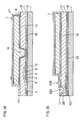
- a plan view showing the structure of one pixel unit of an electromagnetic wave detecting element 10' that is used in an indirect-conversion-type radiation image detection device is shown in Fig. 13 .
- a cross-sectional view along line A-A of Fig. 13 is shown in Fig. 14 .
- sensor portions are provided at the electromagnetic wave detecting element 10', in correspondence with the respective intersection portions of plural scan lines 101' and plural signal lines 3' that are disposed so as to intersect one another.
- the sensor portion includes: a semiconductor layer 6' at which charges are generated due to light being illuminated; an upper electrode 7' that is formed by a light-transmissive, electrically-conductive member at an illumination surface side of the semiconductor layer 6' at which light is illuminated, and that applies bias voltage to the semiconductor layer 6'; and a lower electrode 14' that is formed at the light non-illumination surface side of the semiconductor layer 6', and collects charges that are generated at the semiconductor layer 6'.
- common electrode lines 25' that supply bias voltage to the upper electrodes 7', are disposed at the upper layer of the semiconductor layer 6'.
- the resistance of the common electrode lines 25' must be made to be low in order to supply charges. Therefore, the common electrode lines 25' are formed by using a low-resistance wiring material of Al or Cu, or of mainly Al or Cu.
- US Patent No. 5,777,355 discloses a technique of connecting respective upper electrodes that are formed from transparent, electrically-conductive members, so as to have them function also as common electrode lines.
- an electromagnetic wave detecting element that, by using the technique disclosed in US Patent No. 5,777,355 , connects the respective upper electrodes 7' that are formed from transparent, electrically-conductive members and causes them to function also as common electrode lines, is considered.
- the resistivity of a transparent, electrically-conductive member is very large, and is 50 to 200 times that of a low-resistance wiring material. Accordingly, if the upper electrodes 7' are respectively connected and made to function also as common electrode lines, the wiring load (resistance, capacity) of the common electrode lines increases, and the desired response cannot be realized. Therefore, the upper electrodes 7' cannot be respectively connected and made to function also as common electrode lines.
- the efficiency of utilization of light is mentioned because light is the object of detection of the semiconductor layer 6'.
- the object of detection is any type of electromagnetic waves such as ultraviolet rays or infrared rays.
- the present invention provides an electromagnetic wave detecting element that, although equipped with a common electrode line, can prevent a decrease in the efficiency of utilizing electromagnetic waves at sensor portions.
- a first aspect of the present invention is an electromagnetic wave detecting element that includes: a plurality of sensor portions having: semiconductor layer provided in correspondence with respective intersection portions of a plurality of scan lines and a plurality of signal lines that are disposed so as to intersect one another, the semiconductor layer generating charges by being irradiated by electromagnetic waves expressing an image that is an object of detection, first electrodes formed by electrically-conductive members, that have transmittance with respect to the electromagnetic waves, at irradiation surface sides of the semiconductor layer to which the electromagnetic waves are irradiated, the first electrodes applying bias voltage to the semiconductor layer, and second electrodes formed at non-irradiation surface sides of the semiconductor layer with respect to the electromagnetic waves, the second electrodes collecting the charges that are generated at the semiconductor layer; and a common electrode line formed at an electromagnetic wave downstream side of the sensor portions, and connected to the first electrodes via respective contact holes, and supplying the bias voltage.
- the electromagnetic wave detecting element of the present invention is sensor portions that generate charges due to electromagnetic waves being irradiated.
- the sensor portions that have the semiconductor layer at whose electromagnetic wave irradiation surface sides the first electrodes are formed and at whose electromagnetic wave non-irradiation surface sides the second electrodes are formed, are provided in correspondence with the respective intersection portions of the scan lines and the signal lines.
- bias voltage is supplied to the first electrodes via respective contact holes by the common electrode line that is formed further toward the electromagnetic wave downstream side than the sensor portions.
- the common electrode line that supplies bias voltage to the first electrodes is formed further toward the downstream side of the electromagnetic waves than the sensor portions. Accordingly, shielding of the electromagnetic waves, that are irradiated onto the semiconductor layer, by the common electrode line is eliminated. Therefore, even though the electromagnetic wave detecting element of the present invention of the above-described aspect is provided with a common electrode line, it can prevent a decrease in the efficiency of utilizing electromagnetic waves at the sensor portions.
- the common electrode line may have low resistance compared to the electrically-conductive members that form the first electrodes.
- the common electrode line may be Al or Cu, or may be an alloy or a layered film including Al or Cu.
- the above-described aspect may further include: a first insulating film provided between the plurality of sensor portions and the common electrode line and insulating the sensor portions and the common electrode line, the plurality of contact holes being formed in the first insulating film; and a plurality of contacts whose respective one ends are connected to the first electrodes via the contact holes respectively, and whose other ends are connected to the common electrode line.
- the scan lines may be formed by a wiring layer that is formed at an electromagnetic wave downstream side, via a second insulating film, of a wiring layer at which the common electrode line is formed, and contact holes may be formed in the first insulating film at positions at the irradiation surface sides of regions where the scan lines are formed.
- the first insulating film may be an interlayer insulating film whose film thickness is greater than or equal to 1 ⁇ m. Further, in a seventh aspect of the present invention, in the above-described aspect, the first insulating film may be an interlayer insulating film whose dielectric constant is 2 to 4.
- the above-described aspect may further include a third insulating film that covers at least outer peripheries of the plurality of sensor portions, and in which a plurality of contact holes are formed, wherein one ends of a plurality of contacts are connected to the first electrodes via the contact holes that are formed in the first insulating film and the third insulating film respectively, and other ends of the plurality of contacts are connected to the common electrode line.
- the third insulating film may be an interlayer insulating film whose film thickness is thicker than a film thickness of the sensor portions.
- the above-described aspect may further include a protective insulating film that is formed of an inorganic material and that covers the third insulating film, the contacts, and the first electrodes. Further, in an eleventh aspect of the present invention, the above-described aspect may further include a protective insulating film that is formed of an inorganic material between the first insulating film and the third insulating film.
- the protective insulating film may be an SiNx or SiOx film.
- the contacts may be formed from IZO or ITO. Further, in a fourteenth aspect of the present invention, in the above-described aspect, the contacts may be formed of a same member as the first electrodes.
- the first electrodes may be electrically connected via connection regions to other adjacent first electrodes.
- connection regions may be formed from electrically-conductive members having transmittance with respect to the electromagnetic waves.
- the first electrodes may be connected to other first electrodes that are adjacent along the signal line. Further, in an eighteenth aspect of the present invention, in the above-described aspect, the first electrodes may be connected to other first electrodes that are adjacent along the scan line.
- the electromagnetic waves mean electromagnetic waves that are mainly detected at the sensor portions.
- the light that is emitted by the scintillator corresponds to the electromagnetic waves.
- the side of the semiconductor layer that faces the scintillator is the electromagnetic wave irradiation surface.
- the side opposite the scintillator is the electromagnetic wave non-irradiation surface.
- the scintillator side thereof is called the upstream side, and the opposite side thereof is called the downstream side.
- the common electrode line that supplies bias voltage to the first electrodes and that is formed from a light-shielding, low-resistance wiring material, is formed at the electromagnetic wave downstream side of the sensor portions. Accordingly, an electromagnetic wave detecting element can be provided that, although equipped with a common electrode line, can prevent a decrease in the efficiency of utilizing electromagnetic waves at sensor portions.
- the overall structure of the radiation image detection device 100 relating to a first exemplary embodiment is illustrated in Fig. 1 . However, a scintillator that converts radiation into light is not illustrated.
- the radiation image detection device 100 As shown in Fig. 1 , the radiation image detection device 100 relating to the present exemplary embodiment has an electromagnetic wave detecting element 10.
- the electromagnetic wave detecting element 10 has upper electrode, semiconductor layer, and lower electrode that will be described later.
- a large number of pixels that are structured to include sensor portions 103 and TFT switches 4 are provided in a two-dimensional form at the electromagnetic wave detecting element 10.
- the sensor portion 103 receives light, that is obtained by irradiated radiation being converted at a scintillator, and accumulates charges.
- the TFT switch 4 reads-out the charges accumulated in the sensor portion 103.
- Plural scan lines 101 for turning the TFT switches 4 on and off, and plural signal lines 3 for reading-out the charges accumulated in the sensor portions 103, are provided at the electromagnetic wave detecting element 10 so as to intersect one another.
- the signal detecting circuits 105 incorporate therein, for each of the signal lines 3, an amplifying circuit that amplifies the inputted electric signal. At the signal detecting circuits 105, the electric signals that are inputted from the respective signal lines 3 are amplified by the amplifying circuits and detected. The signal detecting circuits 105 thereby detect the charge amounts accumulated in the respective sensor portions 103 as information of the respective pixels structuring the image.
- the signal detecting circuits 105 and the scan signal controlling device 104 carry out predetermined processings on the electric signals detected at the signal detecting circuits 105. Further, a signal processing device 106 is connected to the signal detecting circuits 105 and the scan signal controlling device 104. The signal processing device 106 outputs control signals expressing signal detecting timings to the signal detecting circuits 105, and outputs control signals expressing scan signal outputting timings to the scan signal controlling device 104.
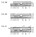
- a plan view showing the structure of one pixel unit of the electromagnetic wave detecting element 10 relating to the present exemplary embodiment is shown in Fig. 2 .
- a cross-sectional view along line A-A of Fig. 2 is shown in Fig. 3A
- a cross-sectional view along line B-B of Fig. 2 is shown in Fig. 3B .
- the scan line 101 and gate electrode 2 are formed on an insulative substrate 1 that is formed from alkaline-free glass or the like, and the scan line 101 and the gate electrode 2 are connected (see Fig. 2 ).
- the wiring layer at which the scan lines 101 and the gate electrodes 2 are formed (hereinafter, this wiring layer is also called a "first signal wiring layer") is formed by using Al or Cu, or a layered film formed mainly of Al or Cu.
- the formation of the wiring layer is not limited to these.
- An insulating film 15 is formed on the entire surface on the scan line 101 and the gate electrode 2, so as to cover the scan line 101 and the gate electrode 2.
- the region of the insulating film 15 that is positioned above the gate electrode 2 works as a gate insulating film at the TFT switch 4.
- the insulating film 15 is formed of, for example, SiN X or the like.
- the insulating film 15 is formed by, for example, CVD (Chemical Vapor Deposition).
- Semiconductor active layer 8 is formed as islands on the gate electrode 2 on the insulating film 15.
- the semiconductor active layer 8 is the channel portion of the TFT switch 4.
- the semiconductor active layer 8 is formed from, for example, an amorphous silicon film.
- a source electrode 9 and a drain electrode 13 are formed at the upper layer thereof. Together with the source electrodes 9 and the drain electrode 13, the signal line 3, and common electrode line 25 that are parallel to the signal line 3, are formed at the wiring layer at which the source electrode 9 and the drain electrode 13 are formed.
- the source electrode 9 is connected to the signal line 3.
- the wiring layer in which the signal lines 3, the source electrodes 9 and the common electrode lines 25 are formed (hereinafter, this wiring layer is also called a "second signal wiring layer") is formed by using Al or Cu, or a layered film formed mainly of Al or Cu. However, the formation of the wiring layer is not limited to these.
- a contact layer (not shown) is formed between, on the one hand, the source electrode 9 and the drain electrode 13, and, on the other hand, the semiconductor active layer 8.
- This contact layer is formed from an impurity-added semiconductor such as an impurity-added amorphous silicon or the like.
- the TFT switch 4 for switching is structured as described above.
- a TFT protecting film layer 11 is formed on substantially the entire surface of the region on the substrate 1 where the pixels are provided (substantially the entire region), so as to cover the semiconductor active layer 8, the source electrodes 9, the drain electrodes 13, the signal lines 3 and the common electrode lines 25.
- the TFT protecting film layer 11 is formed of, for example, SiN X or the like.
- the TFT protecting film layer 11 is formed by, for example, CVD.
- a coating-type interlayer insulating film 12 is formed on the TFT protecting film layer 11.
- a photosensitive organic material e.g., a positive photosensitive acrylic resin: a material in which a naphthoquinonediazide positive photosensitive agent is mixed together with a base polymer formed from a copolymer of methacrylic acid and glycidyl methacrylate, or the like
- a photosensitive organic material e.g., a positive photosensitive acrylic resin: a material in which
- the capacity between the metals that are disposed at the upper layer and the lower layer of the interlayer insulating film 12 is kept low by the interlayer insulating film 12.
- such a material also functions as a flattening film, and also has the effect of flattening the steps of the lower layer. Because the shapes of semiconductor layer 6 that are disposed at the upper layer are flattened thereby, a decrease in the absorption efficiency due to unevenness of the semiconductor layer 6, and an increase in leak current can be suppressed.
- Contact holes 16 and contact holes 22A are formed respectively in the interlayer insulating film 12 and the TFT protecting film layer 11 at positions opposing the drain electrodes 13 and at positions that are at the irradiation surface sides of the regions where the scan lines 101 are formed.
- a lower electrode 14 of the sensor portion 103 is formed on the interlayer insulating film 12, so as to cover the pixel region while filling-in the contact hole 16.
- the drain electrode 13 of the TFT switch 4 is connected to the lower electrode 14.
- the semiconductor layer 6 that will be described later is formed to be thick and around 1 ⁇ m, the material of the lower electrode 14 is not limited provided that it is electrically-conductive. Therefore, the lower electrode 14 can be formed by using an electrically-conductive metal such as an Al-type material, ITO (indium tin oxide), or the like.
- the semiconductor layer 6 is an alloy or a layered film that is formed mainly of a light-shielding metal.
- the semiconductor layer 6 that functions as a photodiode is formed on the lower electrode 14.
- a PIN structure photodiode is employed as the semiconductor layer 6.
- the photodiode is formed by layering an n + layer, an i layer, and a p + layer in that order from the lower layer.
- the lower electrode 14 is made to be larger than the semiconductor layer 6.
- the film thickness of the semiconductor layer 6 is thin (e.g., less than or equal to 0.5 ⁇ m), in order to prevent incidence of light onto the TFT switch 4, it is preferable to place a light-shielding metal to cover the TFT switch 4.
- the interval from the channel portion of the TFT switch 4 to the end portion of the lower electrode 14 that is formed from a light-shielding metal is ensured to be greater than or equal to 5 ⁇ m.
- a protective insulating film 17 is formed on the interlayer insulating film 12 and the semiconductor layer 6, so as to have openings at the respective semiconductor layer 6 portions.
- An upper electrode 7 is formed on the semiconductor layer 6 and the protective insulating film 17, at least so as to cover the opening portion of the protective insulating film 17.
- a material having high light transmittance such as, for example, ITO or IZO (indium zinc oxide) or the like, is used as the upper electrodes 7.
- the upper electrodes 7 is also used as an electrically-conductive member that is connected to the common electrode lines 25 disposed at the lower layer for supplying bias voltage to the upper electrodes 7. As shown in Fig.
- the common electrode line 25 are connected to a contact pad 24 that is formed in the layer of the lower electrode 14 via the contact hole 22A provided in the first interlayer insulating film 12. Further, the upper electrode 7 and the common electrode line 25 are electrically connected by a contact hole 22B, that is provided in the protective insulating film 17, being covered by the upper electrode 7.
- the electrically-conductive member that connects the upper electrodes 7 and the common electrode lines 25 may be formed by a metal of another layer.
- the upper electrode 7 and the semiconductor layer 6 are formed integrally in order to decrease the contact resistance between the semiconductor layer 6 and the upper electrode 7. Therefore, as shown in Fig. 16A and Fig. 16B , the upper electrode 7 and the semiconductor layer 6 are the same shape.
- an electrically-conductive member 26, that is connected to the common electrode line 25, is disposed on the opening portion of the protective insulating film 17 at a layer that is separate from the upper electrode 7.
- a material having high light transmittance such as, for example, ITO or IZO (indium zinc oxide) or the like, is used as this electrically-conductive member 26.
- a scintillator 30 formed of GOS or the like is affixed to the electromagnetic wave detecting element 10 that is formed in this way, by using an adhesive resin 28 having low light absorbance, or the like.
- the gate electrodes 2 and the scan lines 101 are formed on the substrate 1 as the first signal wiring layer ( Fig. 5A ).
- This first signal wiring layer is formed from a low-resistance metal such as Al, an Al alloy or the like, or from a layered film that is layered with a barrier metal layer formed from a high melting point metal.
- the first signal wiring layer is deposited on the substrate 1 by sputtering to a film thickness of around 100 to 300 nm. Thereafter, patterning of a resist film is carried out by a photolithographic technique. Thereafter, the metal film is patterned by wet etching using an etchant for Al or by dry etching. By removing the resist thereafter, the first signal wiring layer is completed.
- the insulating film 15 is formed from SiNx, and the film thickness thereof is 200 to 600 nm.
- the semiconductor active layer 8 is formed from amorphous silicon, and the film thickness thereof is around 20 to 200 nm.
- the contact layers are formed from an impurity-added amorphous silicon, and the film thickness thereof is around 10 to 100 nm. These layers are deposited by P-CVD (Plasma-Chemical Vapor Deposition). Thereafter, in the same way as the first signal wiring layer, patterning of the resist is carried out by a photolithographic technique. Thereafter, the semiconductor active regions are formed by selectively dry etching, with respect to the insulating film 15, the semiconductor active layer 8 and the contact layer that are formed by an impurity-added semiconductor.
- the signal lines 3, the source electrodes 9, the drain electrodes 13, and the common electrode lines 25 are formed as the second signal wiring layer at the top layer of the insulating film 15 and the semiconductor active layer 8 ( Fig. 5C ).
- the second signal wiring layer is formed from a low-resistance metal such as Al, an Al alloy or the like, or from a layered film that is layered with a barrier metal layer formed from a high melting point metal, or from a single layer of a high melting point metal film such as Mo or the like, and the film thickness thereof is around 100 to 300 nm.
- patterning is carried out by a photolithographic technique, and the metal film is patterned by wet etching using an etchant for Al or by dry etching.
- the insulating film 15 is not removed.
- dry etching portions of the contact layers and the semiconductor active layer 8 are removed and channel regions are formed.
- the TFT protecting film layer 11 and the interlayer insulating film 12 are successively formed at the upper layer of the layers that were formed as described above ( Fig. 5D ).
- the TFT protecting film layer 11 and the interlayer insulating film 12 are a single body of an inorganic material, and cases in which they are formed by layering a protective insulating film formed of an inorganic material and an interlayer insulating film formed of an organic material, and cases in which they are formed by a single layer of an interlayer insulating film that is organic.
- the interlayer insulating film 12 that is photosensitive and the TFT protecting film layer 11 that is formed of an inorganic material, in order to stabilize the characteristics of the TFT switches 4 and suppress the electrostatic capacity between the lower electrodes 14 and the common electrode lines 25 at the lower layer.
- the TFT protecting film layer 11 is formed by CVD, the interlayer insulating film 12 material that is photosensitive and is a coating material is coated, and after pre-baking, the steps of exposure and developing are carried out, and thereafter, baking is carried out such that the respective layers are formed.
- the TFT protecting film layer 11 is patterned by a photolithographic technique ( Fig. 5E ). Note that this step is not necessary in cases in which the TFT protecting film layer 11 is not provided.
- an Al-type material or a metal material such as ITO or the like is deposited by sputtering to a film thickness of around 20 to 200 nm on the top layer of the above-described layers.
- patterning is carried out by a photolithographic technique, and patterning is carried out by wet etching using an etchant for metal or the like or by dry etching, so as to form the lower electrodes 14 ( Fig. 5F ).
- n + , i, p + are deposited in order from the lower layer, so as to form the semiconductor layer 6 (see Fig. 5G ).
- the film thickness of the n + layer is 50 to 500 nm
- the film thickness of the i layer is 0.2 to 2 ⁇ m
- the film thickness of the p + layer is 50 to 500 nm.
- the respective layers are layered in order and the semiconductor layer 6 are patterned by a photolithographic technique, and by selectively etching the interlayer insulating film 12 at the lower layer by dry etching or by wet etching, the semiconductor layer 6 are completed.
- the semiconductor layer 6 is formed by layering n + , i, p + in order.
- the semiconductor layer 6 may be a PIN diode by layering p + , i, n + in order.
- the protective insulating film 17 that is formed from an SiNx film is deposited by CVD or the like so as to cover the semiconductor layer 6.
- the film thickness of the protective insulating film 17 is around 100 to 300 nm. Patterning is carried out by a photolithographic technique, and patterning is carried out by dry etching, and opening portions are formed ( Fig. 5H ).
- SiNx is used as an example of the CVD film.
- the protective insulating film 17 is not limited to SiNx, and another material may be applied provided that it is an insulating material.
- connection regions of the upper electrodes 7 and the common electrode lines 25 are formed ( Fig. 5I ).
- the connection regions of the upper electrodes 7 and the common electrode lines 25 are formed by depositing, by sputtering, a transparent electrode material such as ITO or the like on the top layer of the layers that were formed as described above.
- the film thickness of the connection regions is around 20 to 200 nm.
- the connection regions are formed by carrying out patterning by a photolithographic technique, and by patterning the upper electrodes 7 by wet etching using an etchant for ITO or the like or by dry etching. By employing etching selectively at this time, the protective insulating film 17 at the lower layer is not damaged.
- the electromagnetic wave detecting element 10 is formed as shown in Fig. 4 .
- the irradiated X-rays are absorbed by the scintillator 30 and are converted into visible light.
- the X-rays may be irradiated from below in Fig. 4 .
- the X-rays are absorbed by the scintillator 30 and are converted into visible light.
- the light amount generated from the scintillator 30 is 0.5 to 2 ⁇ W/cm 2 in conventional X-ray photography for medical diagnosis. This generated light passes through the layer of the adhesive resin 28, and is illuminated onto the semiconductor layer 6 of the sensor portions 103 that are arranged in the form of an array on the TFT array substrate.
- the semiconductor layer 6 is provided so as to be separated into the respective pixel units.
- a predetermined bias voltage is applied to the semiconductor layer 6 from the upper electrode 7 via the common electrode line 25, and when light is illuminated, charges are generated at the interior of the semiconductor layer 6.
- negative bias voltage is applied to the upper electrode 7. If the film thickness of the i layer is around 1 ⁇ m, the bias voltage that is applied is around -5 to -10 V.
- the signal detecting circuits 105 detect the charge amounts accumulated in the respective sensor portions 103 as information of the respective pixels forming the image. The image information expressed by the X-rays that are irradiated onto the electromagnetic wave detecting element 10 can thereby be obtained.
- the common electrode lines 25 are formed, with respect to the sensor portions 103, at the non-illumination surface side of the visible light from the scintillator 30 (the downstream side of the visible light). Further, at the electromagnetic wave detecting element 10 relating to the present exemplary embodiment, bias voltage is supplied to the upper electrode 7 via the contact holes 22A, 22B.
- a second exemplary embodiment describes a case in which the scan lines 101, the signal lines 3, and the common electrode lines 25 are formed by different wiring layers.
- FIG. 6 A plan view showing the structure of one pixel unit of the electromagnetic wave detecting element 10 relating to the second exemplary embodiment is shown in Fig. 6 . Further, a cross-sectional view along line A-A of Fig. 6 is shown in Fig. 7A , and a cross-sectional view along line B-B of Fig. 6 is shown in Fig. 7B . Description of portions in Fig. 6 and Fig. 7 , that are the same as in Fig. 2 and Fig. 3 , is omitted.
- the scan line 101 and the gate electrode 2 are formed on the substrate 1, and the scan line 101 and the gate electrode 2 are connected (see Fig. 6 ).
- the insulating film 15 is formed on the entire surface on the scan line 101 and the gate electrode 2, so as to cover the scan line 101 and the gate electrode 2.
- the region of the insulating film 15 that is positioned above the gate electrode 2 works as a gate insulating film at the TFT switch 4.
- the semiconductor active layer 8 is formed as islands on the gate electrode 2 on the insulating film 15.
- the common electrode line 25 are formed, parallel to the signal line 3, at the upper layer of the insulating film 15 at which the source electrode 9 and the drain electrode 13 are formed at the upper layer of the semiconductor active layer 8.
- a first TFT protecting film layer 11A is formed on the source electrode 9, the drain electrode 13 and the common electrode line 25 on substantially the entire surface of the region on the substrate 1 where the pixels are provided, so as to cover the source electrode 9, the drain electrode 13 and the common electrode line 25.
- the signal line 3, contact pad 24A and contact pad 38 are formed on the first TFT protecting film layer 11 A.
- the signal line 3 is connected to the source electrode 9 via a contact hole 36 (see Fig. 6 ).
- the signal line 3 is connected to the common electrode lines 25 via the contact pad 24A and the contact hole 22A.
- the contact pad 38 is connected to the drain electrode 13 via a contact hole 40.
- a second TFT protecting film layer 11B is formed on the signal lines 3, the contact pads 24A and the contact pads 38 on substantially the entire surface of the region on the substrate 1 where the pixels are provided, so as to cover the signal lines 3, the contact pads 24A and the contact pads 38. Further, the coating-type interlayer insulating film 12 is formed on the second TFT protecting film layer 11B.
- Contact hole 22C and the contact hole 16 are formed respectively in the second TFT protecting film layer 11B and the interlayer insulating film 12 at positions opposing the contact pads 24A and at positions where the contact pad 38 of the illumination surface sides of the regions where the scan line 101 are formed are provided.
- the lower electrode 14, the semiconductor layer 6 and the upper electrode 7 of the sensor portion 103, and the protective insulating film 17 are formed on the interlayer insulating film 12.
- the contact pad 24A is connected to the contact pad 24B, that is formed in the layer of the lower electrode 14, via the contact hole 22C provided in the first interlayer insulating film 12. Further, by covering the top of the contact hole 22B provided in the protective insulating film 17 with the upper electrode 7, the upper electrode 7 and the common electrode line 25 are electrically connected.
- the scintillator 30 formed of GOS or the like is affixed to the electromagnetic wave detecting element 10 that is formed in this way, by using the adhesive resin 28 having low light absorbance, or the like.
- the gate electrodes 2 and the scan lines 101 are formed on the substrate 1.
- the insulating film 15 is formed on the entire surface so as to cover the gate electrodes 2 and the scan lines 101.
- the semiconductor active layer 8 and the contact layers are formed on the insulating film 15 ( Fig. 9A ).
- the source electrodes 9 and the drain electrodes 13 are formed at the top layer of the semiconductor active layer 8. Then, the common electrode lines 25 are formed on the insulating film 15 ( Fig. 9B ).
- the first TFT protecting film layer 11A is formed on substantially the entire surface, so as to cover the source electrodes 9, the drain electrodes 13, and the common electrode lines 25. Subsequently, the first TFT protecting film layer 11A is patterned by a photolithographic technique ( Fig. 9C ).
- the signal lines 3, the contact pads 24A and the contact pads 38 are formed on the first TFT protecting film layer 11A ( Fig. 9D ).
- the second TFT protecting film layer 11B and the interlayer insulating film 12 are successively formed on the top surface of the layers that are formed as described above ( Fig. 9E ).
- the second TFT protecting film layer 11B is patterned by a photolithographic technique ( Fig. 9F ).
- an Al-type material or a metal material such as ITO or the like is deposited by sputtering on the top layer of the aforementioned layer, and the lower electrodes 14 are formed by patterning ( Fig. 9G ).
- the semiconductor layer 6 is formed on the interlayer insulating film 12 ( Fig. 9H ). Moreover, the protective insulating film 17 is formed ( Fig. 9I ). Then, the connection regions of the upper electrodes 7 and the common electrode lines 25 are formed ( Fig. 9J ).
- the scan lines 101, the signal lines 3, and the common electrode lines 25 are formed at different wiring layers.
- connection regions of the upper electrodes 7 and the common electrode lines 25 are formed on the protective insulating film 17.
- disconnection or the like of the connection regions arises due to changes in the steep angle of the protective insulating film 17 at the lower layer, or cracking, or the like.
- the third exemplary embodiment describes a case in which an interlayer insulating film 18 is further formed at the peripheries of the respective semiconductor layer 6.
- FIG. 17 A plan view showing the structure of one pixel unit of the electromagnetic wave detecting element 10 relating to the third exemplary embodiment is shown in Fig. 17 . Further, a cross-sectional view along line A-A of Fig. 17 is shown in Fig. 18A , and a cross-sectional view along line B-B of Fig. 17 is shown in Fig. 18B . Descriptions of portions in Fig. 17 and Fig. 18 , that are the same as in Fig. 2 and Fig. 3 , are omitted.
- the coating-type interlayer insulating film 18 is formed on the interlayer insulating film 12, so as to cover the outer peripheries of the respective semiconductor layer 6 while having openings at the respective semiconductor layer 6 portions.
- the interlayer insulating film 18 is formed of a photosensitive organic material having low permittivity, and is thicker than the semiconductor layer 6 of the sensor portions 103, and is formed to a film thickness of 1 to 4 ⁇ m.
- the contact holes 22B are formed in the interlayer insulating film 18, respectively at the positions of the contact pads 24.
- the contact hole 22B is formed in a conical shape (a taper shape) at which the diameter becomes smaller in the direction of thickness.
- the contact hole 22B is formed such that an angle ⁇ of the inner surface with respect to the cone axis is less than or equal to 60°, and is greater than the angle with respect to the perpendicular direction of the edge of the semiconductor layer 6.
- the upper electrodes 7 are formed on the semiconductor layer 6 and the interlayer insulating film 18, so as to cover at least the opening portion of the interlayer insulating film 18.
- the upper electrodes 7 also serves as an electrically-conductive member that is connected to the common electrode lines 25 that are disposed at the lower layer for supplying bias voltage to the upper electrodes 7.
- the common electrode lines 25 are connected, via the contact holes 22A provided in the first interlayer insulating film 12, to the contact pads 24 that is formed at the layer of the lower electrodes 14. Further, the upper electrodes 7 and the common electrode lines 25 are electrically connected by covering the contact holes 22B, that is provided in the interlayer insulating film 18, by the upper electrodes 7.
- the protective insulating film 17 is formed on substantially the entire surfaces of the interlayer insulating film 18 and the upper electrodes 7.
- the scintillator 30 formed of GOS or the like is affixed to the electromagnetic wave detecting element 10 that is formed in this way, by using the adhesive resin 28 having low light absorbance, or the like.
- Fig. 19A through Fig. 19G are the same portions as Fig. 5A through Fig. 5G , description thereof is omitted. Further, with regard to the materials, the film thicknesses and the methods of forming the respective layers, description of portions that are the same as in the first exemplary embodiment is omitted.
- the interlayer insulating film 18 is successively formed on the interlayer insulating film 12 ( Fig. 19H ).
- the interlayer insulating film 18 is formed by coating a material that is photosensitive and is a coating material, and after pre-baking, carrying out the steps of exposure and developing, and thereafter, carrying out baking, and forming the contact holes 22B as well.
- connection regions of the upper electrodes 7 and the common electrode lines 25 are formed on the interlayer insulating film 18.
- the protective insulating film 17 is formed on substantially the entire surface of the upper electrodes 7 ( Fig. 19I ).
- the angle ⁇ of the inner surface of the contact hole 22B can be made to be gentle as shown in Fig. 18B . Therefore, the occurrence of disconnection or the like of the connected portions of the upper electrodes 7 and the common electrode lines 25 can be suppressed.
- IZO or ITO it is easy for disconnection due to changes in the steep angle, cracking or the like, to arise. Therefore, utilizing a structure such as that of the present third exemplary embodiment is effective.
- the moisture permeability is high and moisture within the air penetrates in, leak current from the semiconductor layer 6 increases, and the device characteristics of the electromagnetic wave detecting element 10 may change.
- the protective insulating film 17 as in the present third exemplary embodiment, moisture within the air penetrating into the interlayer insulating film 18 can be suppressed.
- the third exemplary embodiment describes a case in which the interlayer insulating film 18 is provided at the peripheries of the respective semiconductor layer 6.
- the interlayer insulating film 18 may be provided so as to cover the top surfaces of the respective semiconductor layer 6, and contact holes may be formed at the top surfaces of the respective semiconductor layer 6.
- a protective insulating film 19 may be formed between the interlayer insulating film 12 and the interlayer insulating film 18 as shown in Fig. 20A and Fig. 20B .
- This case can be realized by forming the interlayer insulating film 19 that is formed from an inorganic material by CVD, for example, on the interlayer insulating film 12 and the semiconductor layer 6 that are formed in the process of Fig. 19G , and thereafter, carrying out the process of above-described Fig. 19H so as to form the interlayer insulating film 18, and patterning the protective insulating film 19 at the contact hole 22B portions and the portions of connection with the upper electrodes 7 by a photolithographic technique. Due thereto, at the time of forming the contact holes 22B in the interlayer insulating film 18, the residue that is generated within the contact holes 22B can be removed at the time of patterning the protective insulating film 19.
- the contact holes that connect the upper electrodes 7 and the common electrode lines 25 are disposed between adjacent sensor portions 103. Therefore, a decrease in the surface area of the light-receiving regions of the sensor portions 103 (the fill factor) can be prevented.
- the sensor portions 103 are separated at the positions of the signal lines 3 and the scan lines 101, in order to decrease the wiring loads of the signal lines 3 and the scan lines 101. Accordingly, the contact holes are disposed above the signal lines 3 or above the scan lines 101. However, in order to decrease image detecting noise, it is preferable that the contact holes be disposed above the scan lines 101.
- the common electrode lines 25 are formed at the non-irradiation surface side of the lower electrode 14, via the insulating films (the TFT protecting film layer 11 and the interlayer insulating film 12 in the first and third exemplary embodiments, and the TFT protecting film layers 11 A, 11B and the interlayer insulating film 12 in the second exemplary embodiment). Therefore, the capacity between the lower electrodes 14 and the common electrode lines 25 decreases, and the switching noise of the TFT switches 4 can be decreased. Namely, the switching noise increases proportionately to the capacity. For example, in a case in which the insulating film is SiNx or the like, there are limits of around 7 for the dielectric constant and around 0.5 ⁇ m for the film thickness.
- the capacity between the lower electrode 14 and the common electrode line 25 is large.
- the capacity becomes, for example, 1/8. Accordingly, the capacity is small as compared with the capacity of the sensor portion 103, and the switching noise is of an extent that can be ignored.
- the common electrode lines 25 are formed parallel to the signal lines 3. Therefore, the signal lines 3 do not intersect the common electrode lines 25. Accordingly, an increase in the electrostatic capacity of the lines due to the signal lines 3 and the common electrode lines 25 intersecting can be prevented. Thus, electronic noise that is generated at the signal lines 3 can be reduced.
- portions of the upper electrode 7 extend along the signal line 3, and are connected to the upper electrodes 7 of the other pixels that are adjacent along the signal line 3 so as to elongate the common electrode line 25. Due thereto, even in a case in which poor contact arises at a contact hole that connects the upper electrode 7 and the common electrode line 25, bias voltage can be applied to the upper electrode 7 from the adjacent pixels. Therefore, poor operation of the sensor portion 103 can be suppressed.
- the above-described respective exemplary embodiments describe cases in which the upper electrode 7 is connected to the upper electrodes 7 of the other pixels that are adjacent along the signal line 3.
- the present invention is not limited to the same.
- the upper electrode 7 may be also be connected to the upper electrodes 7 of the other pixels that are adjacent along the scan line 101. Due thereto, the occurrence of artifacts caused by the electrode potential distribution along the scan line 101 direction can be suppressed. Note that, it is possible for the upper electrode 7 to be connected to only the upper electrodes 7 of the other pixels that are adjacent along the scan line 101.
- the upper electrode 7 may be made to be independent and not connected to the upper electrodes 7 of other pixels.
- the common electrode lines 25 are formed in parallel to the signal lines 3.
- the present invention is not limited thereto.
- the common electrode lines 25 may be formed parallel to the scan lines 101.
- the above respective exemplary embodiments describe cases in which the present invention is applied to the indirect-conversion-type electromagnetic wave detecting element 10 that once converts radiation into light at the scintillator 30, and converts the converted light into charges at the semiconductor layer 6 and accumulates the charges.
- the present invention is not limited thereto, and may be applied to, for example, a direct-conversion-type electromagnetic wave detecting element that directly converts radiation into charges at a semiconductor layer of amorphous silicon or the like, and accumulates the charges.
- the indirect-conversion-type electromagnetic wave detecting element 10 radiation is converted into light at the scintillator 30, and the light converted at the scintillator 30 is received, and charges are accumulated at the sensor portions 103. Therefore, in the case of an indirect-conversion-type electromagnetic wave detecting element, the electromagnetic waves, that express the image that is the object of detection of the sensor portions of the present invention, are light. Further, at the electromagnetic wave detecting element 10 relating to the present exemplary embodiment, even in a case in which radiation is irradiated from the substrate 1 side, the radiation is converted into light at the scintillator 30, the converted light is illuminated onto the sensor portion 103, and charges are generated at the semiconductor layer 6.
- the irradiation surface side of the semiconductor layer 6, at which the electromagnetic waves that are the object of detection are irradiated is the scintillator 30 side, and the non-irradiation surface side is the substrate 1 side.
- a direct-conversion-type electromagnetic wave detecting element radiation is converted directly into charges at a semiconductor layer.
- the electromagnetic waves, that express the image that is the object of detection of the sensor portion of the present invention are radiation.
- the radiation is converted directly into charges at the semiconductor layer. Therefore, the irradiation surface side of the semiconductor layer, at which the electromagnetic waves are irradiated, is the side at which the radiation is irradiated, and the non-irradiation surface side is the side at which radiation is not irradiated.
- the irradiation surface side of the semiconductor layer, at which the electromagnetic waves are irradiated is the substrate side
- the non-irradiation surface side is the side of the semiconductor layer that is opposite the side where the substrate is located.
- the above respective exemplary embodiments describe cases in which the present invention is applied to the radiation image detection device 100 that detects an image by detecting X-rays as the electromagnetic waves that are the object of detection.
- the present invention is not limited thereto.
- the electromagnetic waves that are the object of detection may be, for example, any of visible light, ultraviolet rays, infrared rays, and the like.
- the structure (see Fig. 1 ) of the radiation image detection device 100 described in the respective exemplary embodiments and the structures ( Fig. 2 through Fig. 12 ) of the electromagnetic wave detecting elements 10 are examples, and appropriate changes can be made thereto within a scope that does not deviate from the gist of the present invention.
Landscapes
- Solid State Image Pick-Up Elements (AREA)
- Measurement Of Radiation (AREA)
- Light Receiving Elements (AREA)
- Transforming Light Signals Into Electric Signals (AREA)
Priority Applications (1)
| Application Number | Priority Date | Filing Date | Title |
|---|---|---|---|
| EP14154260.5A EP2731136B1 (de) | 2008-01-29 | 2009-01-22 | Element zur Detektion elektromagnetischer Wellen |
Applications Claiming Priority (3)
| Application Number | Priority Date | Filing Date | Title |
|---|---|---|---|
| JP2008017743 | 2008-01-29 | ||
| JP2008093858 | 2008-03-31 | ||
| JP2008209179A JP5185013B2 (ja) | 2008-01-29 | 2008-08-15 | 電磁波検出素子 |
Related Child Applications (2)
| Application Number | Title | Priority Date | Filing Date |
|---|---|---|---|
| EP14154260.5A Division-Into EP2731136B1 (de) | 2008-01-29 | 2009-01-22 | Element zur Detektion elektromagnetischer Wellen |
| EP14154260.5A Division EP2731136B1 (de) | 2008-01-29 | 2009-01-22 | Element zur Detektion elektromagnetischer Wellen |
Publications (3)
| Publication Number | Publication Date |
|---|---|
| EP2086006A2 true EP2086006A2 (de) | 2009-08-05 |
| EP2086006A3 EP2086006A3 (de) | 2011-08-03 |
| EP2086006B1 EP2086006B1 (de) | 2016-09-07 |
Family
ID=40626776
Family Applications (2)
| Application Number | Title | Priority Date | Filing Date |
|---|---|---|---|
| EP14154260.5A Active EP2731136B1 (de) | 2008-01-29 | 2009-01-22 | Element zur Detektion elektromagnetischer Wellen |
| EP09000872.3A Active EP2086006B1 (de) | 2008-01-29 | 2009-01-22 | Element zur Detektion elektromagnetischer Wellen |
Family Applications Before (1)
| Application Number | Title | Priority Date | Filing Date |
|---|---|---|---|
| EP14154260.5A Active EP2731136B1 (de) | 2008-01-29 | 2009-01-22 | Element zur Detektion elektromagnetischer Wellen |
Country Status (5)
| Country | Link |
|---|---|
| US (2) | US8174087B2 (de) |
| EP (2) | EP2731136B1 (de) |
| JP (1) | JP5185013B2 (de) |
| CN (2) | CN102629618B (de) |
| TW (2) | TWI404197B (de) |
Cited By (4)
| Publication number | Priority date | Publication date | Assignee | Title |
|---|---|---|---|---|
| EP2330626A1 (de) * | 2009-12-04 | 2011-06-08 | Carestream Health, Inc. | Koplanare Pixelarchitektur mit hohem Füllfaktor |
| EP2530716A1 (de) * | 2011-05-31 | 2012-12-05 | Canon Kabushiki Kaisha | Herstellungsverfahren für eine Erkennungsvorrichtung, Erkennungsvorrichtung und Erkennungssystem |
| WO2013115841A1 (en) | 2012-01-30 | 2013-08-08 | Jun Seung Ik | Radiation detecting panel |
| US9515118B2 (en) | 2012-01-30 | 2016-12-06 | Rayence Co., Ltd. | Radiation detecting panel |
Families Citing this family (23)
| Publication number | Priority date | Publication date | Assignee | Title |
|---|---|---|---|---|
| JP5439984B2 (ja) * | 2009-07-03 | 2014-03-12 | ソニー株式会社 | 光電変換装置および放射線撮像装置 |
| TWI424574B (zh) * | 2009-07-28 | 2014-01-21 | Prime View Int Co Ltd | 數位x光探測面板及其製作方法 |
| JP5537135B2 (ja) * | 2009-11-30 | 2014-07-02 | 三菱電機株式会社 | 光電変換装置の製造方法 |
| KR101084265B1 (ko) * | 2009-12-18 | 2011-11-17 | 삼성모바일디스플레이주식회사 | 엑스레이 검출기 |
| JP5583452B2 (ja) * | 2010-03-31 | 2014-09-03 | 富士フイルム株式会社 | 電磁波情報検出装置および電磁波情報検出方法 |
| KR101736321B1 (ko) | 2010-12-22 | 2017-05-17 | 삼성디스플레이 주식회사 | 엑스레이 검출기용 박막 트랜지스터 어레이 기판 및 엑스레이 검출기 |
| JP6095276B2 (ja) * | 2011-05-31 | 2017-03-15 | キヤノン株式会社 | 検出装置の製造方法、その検出装置及び検出システム |
| JP2013235935A (ja) * | 2012-05-08 | 2013-11-21 | Canon Inc | 検出装置の製造方法、その検出装置及び検出システム |
| JPWO2013180076A1 (ja) | 2012-05-30 | 2016-01-21 | 富士フイルム株式会社 | 放射線画像撮影装置、放射線画像撮影システム、放射線画像撮影装置の制御方法、及び放射線画像撮影装置の制御プログラム |
| KR101965259B1 (ko) * | 2012-07-27 | 2019-08-08 | 삼성디스플레이 주식회사 | 엑스선 검출기 |
| CN102856441B (zh) * | 2012-09-14 | 2015-03-11 | 京东方科技集团股份有限公司 | X射线探测器背板的制造方法及pin光电二极管的制造方法 |
| JP5709810B2 (ja) | 2012-10-02 | 2015-04-30 | キヤノン株式会社 | 検出装置の製造方法、その検出装置及び検出システム |
| JP2014110352A (ja) * | 2012-12-03 | 2014-06-12 | Canon Inc | 検出装置の製造方法 |
| JP6389685B2 (ja) * | 2014-07-30 | 2018-09-12 | キヤノン株式会社 | 撮像装置、および、撮像システム |
| WO2016167179A1 (ja) * | 2015-04-13 | 2016-10-20 | シャープ株式会社 | 撮像パネル、及びそれを備えたx線撮像装置 |
| US20190115385A1 (en) * | 2016-04-01 | 2019-04-18 | Sharp Kabushiki Kaisha | Photoelectric converter and x-ray detector |
| JP2019110159A (ja) * | 2017-12-15 | 2019-07-04 | シャープ株式会社 | アクティブマトリクス基板、及びそれを備えたx線撮像パネル |
| US11024664B2 (en) * | 2018-07-30 | 2021-06-01 | Sharp Kabushiki Kaisha | Imaging panel |
| KR102608581B1 (ko) * | 2018-10-18 | 2023-11-30 | 엘지디스플레이 주식회사 | 고해상도 디지털 엑스레이 검출기용 박막 트랜지스터 어레이 기판 및 이를 포함하는 고해상도 디지털 엑스레이 검출기 |
| CN111106134B (zh) * | 2018-10-29 | 2023-08-08 | 夏普株式会社 | 有源矩阵基板以及具备其的x射线拍摄面板 |
| JP2022043369A (ja) * | 2018-12-26 | 2022-03-16 | ソニーセミコンダクタソリューションズ株式会社 | 半導体装置および電子機器 |
| US12021092B2 (en) * | 2020-04-17 | 2024-06-25 | Beijing Boe Sensor Technology Co., Ltd. | Flat panel detector substrate and manufacturing method thereof, and flat panel detector |
| JP7449264B2 (ja) * | 2021-08-18 | 2024-03-13 | 株式会社東芝 | 放射線検出器 |
Citations (2)
| Publication number | Priority date | Publication date | Assignee | Title |
|---|---|---|---|---|
| US5777355A (en) | 1996-12-23 | 1998-07-07 | General Electric Company | Radiation imager with discontinuous dielectric |
| JP2000137080A (ja) | 1998-08-28 | 2000-05-16 | Fuji Photo Film Co Ltd | 放射線画像検出装置 |
Family Cites Families (13)
| Publication number | Priority date | Publication date | Assignee | Title |
|---|---|---|---|---|
| JPH02128468A (ja) * | 1988-11-08 | 1990-05-16 | Fujitsu Ltd | 固体撮像装置及びその製造方法 |
| JPH02139525A (ja) * | 1988-11-21 | 1990-05-29 | Fuji Electric Co Ltd | 表示パネルのアクティブマトリックス基板 |
| US5563421A (en) * | 1995-06-07 | 1996-10-08 | Sterling Diagnostic Imaging, Inc. | Apparatus and method for eliminating residual charges in an image capture panel |
| JP4271268B2 (ja) * | 1997-09-20 | 2009-06-03 | 株式会社半導体エネルギー研究所 | イメージセンサおよびイメージセンサ一体型アクティブマトリクス型表示装置 |
| JP4011734B2 (ja) * | 1998-06-02 | 2007-11-21 | キヤノン株式会社 | 2次元光センサ、それを用いた放射線検出装置及び放射線診断システム |
| US6724010B1 (en) * | 2000-08-03 | 2004-04-20 | General Electric Company | Solid state imager having gated photodiodes and method for making same |
| US6535576B2 (en) * | 2000-12-29 | 2003-03-18 | Ge Medical Systems Global Technology Company, Llc | Enhanced digital detector and system and method incorporating same |
| JP4376522B2 (ja) * | 2003-01-24 | 2009-12-02 | シャープ株式会社 | 電磁波検出器 |
| FR2852147B1 (fr) * | 2003-03-06 | 2005-09-30 | Commissariat Energie Atomique | Matrice de pixels detecteurs integree sur circuit de lecture de charges |
| US20050184244A1 (en) * | 2004-02-25 | 2005-08-25 | Shimadzu Corporation | Radiation detector and light or radiation detector |
| JP2006049873A (ja) * | 2004-07-06 | 2006-02-16 | Fuji Photo Film Co Ltd | 機能素子 |
| US7651877B2 (en) * | 2004-10-28 | 2010-01-26 | Sharp Kabushiki Kaisha | Two-dimensional image detecting apparatus and method for manufacturing the same |
| US7759680B2 (en) * | 2005-11-30 | 2010-07-20 | General Electric Company | Thin-film transistor and diode array for an imager panel or the like |
-
2008
- 2008-08-15 JP JP2008209179A patent/JP5185013B2/ja active Active
-
2009
- 2009-01-21 CN CN201210120733.XA patent/CN102629618B/zh active Active
- 2009-01-21 CN CN2009100048391A patent/CN101499481B/zh active Active
- 2009-01-22 EP EP14154260.5A patent/EP2731136B1/de active Active
- 2009-01-22 TW TW098102361A patent/TWI404197B/zh active
- 2009-01-22 US US12/320,225 patent/US8174087B2/en active Active
- 2009-01-22 EP EP09000872.3A patent/EP2086006B1/de active Active
- 2009-01-22 TW TW102116348A patent/TWI515881B/zh active
-
2012
- 2012-04-05 US US13/439,890 patent/US8436442B2/en active Active
Patent Citations (2)
| Publication number | Priority date | Publication date | Assignee | Title |
|---|---|---|---|---|
| US5777355A (en) | 1996-12-23 | 1998-07-07 | General Electric Company | Radiation imager with discontinuous dielectric |
| JP2000137080A (ja) | 1998-08-28 | 2000-05-16 | Fuji Photo Film Co Ltd | 放射線画像検出装置 |
Cited By (9)
| Publication number | Priority date | Publication date | Assignee | Title |
|---|---|---|---|---|
| EP2330626A1 (de) * | 2009-12-04 | 2011-06-08 | Carestream Health, Inc. | Koplanare Pixelarchitektur mit hohem Füllfaktor |
| KR20110063374A (ko) * | 2009-12-04 | 2011-06-10 | 케어스트림 헬스 인코포레이티드 | 픽셀 및 이를 포함하는 이미징 어레이 및 방사선 이미징 시스템 |
| CN102142447A (zh) * | 2009-12-04 | 2011-08-03 | 卡尔斯特里姆保健公司 | 共面高填充系数的像素架构 |
| KR101694550B1 (ko) | 2009-12-04 | 2017-01-09 | 케어스트림 헬스 인코포레이티드 | 픽셀 및 이를 포함하는 이미징 어레이 및 방사선 이미징 시스템 |
| EP2530716A1 (de) * | 2011-05-31 | 2012-12-05 | Canon Kabushiki Kaisha | Herstellungsverfahren für eine Erkennungsvorrichtung, Erkennungsvorrichtung und Erkennungssystem |
| US8866093B2 (en) | 2011-05-31 | 2014-10-21 | Canon Kabushiki Kaisha | Detection device manufacturing method, detection device, and detection system |
| WO2013115841A1 (en) | 2012-01-30 | 2013-08-08 | Jun Seung Ik | Radiation detecting panel |
| EP2810058A4 (de) * | 2012-01-30 | 2015-08-19 | Seung Ik Jun | Strahlungsdetektionstafel |
| US9515118B2 (en) | 2012-01-30 | 2016-12-06 | Rayence Co., Ltd. | Radiation detecting panel |
Also Published As
| Publication number | Publication date |
|---|---|
| US20120187464A1 (en) | 2012-07-26 |
| EP2086006B1 (de) | 2016-09-07 |
| CN101499481B (zh) | 2012-06-13 |
| EP2731136B1 (de) | 2020-01-15 |
| JP5185013B2 (ja) | 2013-04-17 |
| US20090189231A1 (en) | 2009-07-30 |
| EP2731136A8 (de) | 2014-08-06 |
| TW201336059A (zh) | 2013-09-01 |
| US8174087B2 (en) | 2012-05-08 |
| CN102629618A (zh) | 2012-08-08 |
| TWI515881B (zh) | 2016-01-01 |
| CN101499481A (zh) | 2009-08-05 |
| JP2009267326A (ja) | 2009-11-12 |
| TWI404197B (zh) | 2013-08-01 |
| EP2086006A3 (de) | 2011-08-03 |
| EP2731136A1 (de) | 2014-05-14 |
| CN102629618B (zh) | 2015-05-06 |
| TW200939460A (en) | 2009-09-16 |
| US8436442B2 (en) | 2013-05-07 |
Similar Documents
| Publication | Publication Date | Title |
|---|---|---|
| EP2086006B1 (de) | Element zur Detektion elektromagnetischer Wellen | |
| US9520438B2 (en) | Electromagnetic wave detecting element | |
| US7944010B2 (en) | Electromagnetic wave detecting element | |
| JP5448877B2 (ja) | 放射線検出器 | |
| US9735183B2 (en) | TFT flat sensor and manufacturing method therefor | |
| US20130048861A1 (en) | Radiation detector, radiation detector fabrication method, and radiographic image capture device | |
| JP2009212120A (ja) | 電磁波検出素子 | |
| US20130048862A1 (en) | Radiation detector, radiation detector fabrication method, and radiographic image capture device | |
| US20110073979A1 (en) | Detection element | |
| KR101218089B1 (ko) | 디지털 엑스레이 디텍터 및 그 제조방법 | |
| US8274057B2 (en) | Detection element | |
| JP2014122903A (ja) | 放射線検出器および放射線画像撮影装置 | |
| JP5456185B2 (ja) | 電磁波検出素子 | |
| JP5689986B2 (ja) | 電磁波検出素子 |
Legal Events
| Date | Code | Title | Description |
|---|---|---|---|
| PUAI | Public reference made under article 153(3) epc to a published international application that has entered the european phase |
Free format text: ORIGINAL CODE: 0009012 |
|
| AK | Designated contracting states |
Kind code of ref document: A2 Designated state(s): AT BE BG CH CY CZ DE DK EE ES FI FR GB GR HR HU IE IS IT LI LT LU LV MC MK MT NL NO PL PT RO SE SI SK TR |
|
| AX | Request for extension of the european patent |
Extension state: AL BA RS |
|
| PUAL | Search report despatched |
Free format text: ORIGINAL CODE: 0009013 |
|
| AK | Designated contracting states |
Kind code of ref document: A3 Designated state(s): AT BE BG CH CY CZ DE DK EE ES FI FR GB GR HR HU IE IS IT LI LT LU LV MC MK MT NL NO PL PT RO SE SI SK TR |
|
| AX | Request for extension of the european patent |
Extension state: AL BA RS |
|
| RIC1 | Information provided on ipc code assigned before grant |
Ipc: H01L 27/146 20060101AFI20110629BHEP |
|
| 17P | Request for examination filed |
Effective date: 20120124 |
|
| AKX | Designation fees paid |
Designated state(s): DE FR NL |
|
| 17Q | First examination report despatched |
Effective date: 20120328 |
|
| GRAP | Despatch of communication of intention to grant a patent |
Free format text: ORIGINAL CODE: EPIDOSNIGR1 |
|
| INTG | Intention to grant announced |
Effective date: 20160415 |
|
| RIN1 | Information on inventor provided before grant (corrected) |
Inventor name: OKADA, YOSHIHIRO |
|
| GRAS | Grant fee paid |
Free format text: ORIGINAL CODE: EPIDOSNIGR3 |
|
| GRAA | (expected) grant |
Free format text: ORIGINAL CODE: 0009210 |
|
| AK | Designated contracting states |
Kind code of ref document: B1 Designated state(s): DE FR NL |
|
| REG | Reference to a national code |
Ref country code: DE Ref legal event code: R096 Ref document number: 602009040897 Country of ref document: DE |
|
| REG | Reference to a national code |
Ref country code: NL Ref legal event code: FP |
|
| REG | Reference to a national code |
Ref country code: FR Ref legal event code: PLFP Year of fee payment: 9 |
|
| REG | Reference to a national code |
Ref country code: DE Ref legal event code: R097 Ref document number: 602009040897 Country of ref document: DE |
|
| PLBE | No opposition filed within time limit |
Free format text: ORIGINAL CODE: 0009261 |
|
| STAA | Information on the status of an ep patent application or granted ep patent |
Free format text: STATUS: NO OPPOSITION FILED WITHIN TIME LIMIT |
|
| 26N | No opposition filed |
Effective date: 20170608 |
|
| REG | Reference to a national code |
Ref country code: FR Ref legal event code: PLFP Year of fee payment: 10 |
|
| PGFP | Annual fee paid to national office [announced via postgrant information from national office to epo] |
Ref country code: NL Payment date: 20191212 Year of fee payment: 12 |
|
| REG | Reference to a national code |
Ref country code: NL Ref legal event code: MM Effective date: 20210201 |
|
| PG25 | Lapsed in a contracting state [announced via postgrant information from national office to epo] |
Ref country code: NL Free format text: LAPSE BECAUSE OF NON-PAYMENT OF DUE FEES Effective date: 20210201 |
|
| P01 | Opt-out of the competence of the unified patent court (upc) registered |
Effective date: 20230515 |
|
| PGFP | Annual fee paid to national office [announced via postgrant information from national office to epo] |
Ref country code: FR Payment date: 20231212 Year of fee payment: 16 |
|
| REG | Reference to a national code |
Ref country code: DE Ref legal event code: R079 Ref document number: 602009040897 Country of ref document: DE Free format text: PREVIOUS MAIN CLASS: H01L0027146000 Ipc: H10F0039180000 |
|
| PG25 | Lapsed in a contracting state [announced via postgrant information from national office to epo] |
Ref country code: FR Free format text: LAPSE BECAUSE OF NON-PAYMENT OF DUE FEES Effective date: 20250131 |
|
| PGFP | Annual fee paid to national office [announced via postgrant information from national office to epo] |
Ref country code: DE Payment date: 20251203 Year of fee payment: 18 |