EP2086016A2 - Solarzellenmodul - Google Patents
Solarzellenmodul Download PDFInfo
- Publication number
- EP2086016A2 EP2086016A2 EP09250254A EP09250254A EP2086016A2 EP 2086016 A2 EP2086016 A2 EP 2086016A2 EP 09250254 A EP09250254 A EP 09250254A EP 09250254 A EP09250254 A EP 09250254A EP 2086016 A2 EP2086016 A2 EP 2086016A2
- Authority
- EP
- European Patent Office
- Prior art keywords
- solar cell
- high refractivity
- light
- tilted
- cell module
- Prior art date
- Legal status (The legal status is an assumption and is not a legal conclusion. Google has not performed a legal analysis and makes no representation as to the accuracy of the status listed.)
- Withdrawn
Links
- 238000007789 sealing Methods 0.000 claims abstract description 35
- 238000006243 chemical reaction Methods 0.000 claims description 79
- 239000000969 carrier Substances 0.000 claims description 8
- 229920002521 macromolecule Polymers 0.000 claims description 6
- 229920000642 polymer Polymers 0.000 claims description 5
- 239000000463 material Substances 0.000 description 31
- 229920005989 resin Polymers 0.000 description 20
- 239000011347 resin Substances 0.000 description 20
- 238000000034 method Methods 0.000 description 18
- 230000000694 effects Effects 0.000 description 10
- 229920001187 thermosetting polymer Polymers 0.000 description 9
- 230000000052 comparative effect Effects 0.000 description 8
- 239000004065 semiconductor Substances 0.000 description 7
- 239000011521 glass Substances 0.000 description 6
- 238000004519 manufacturing process Methods 0.000 description 6
- 238000003825 pressing Methods 0.000 description 5
- 239000004642 Polyimide Substances 0.000 description 4
- GWEVSGVZZGPLCZ-UHFFFAOYSA-N Titan oxide Chemical compound O=[Ti]=O GWEVSGVZZGPLCZ-UHFFFAOYSA-N 0.000 description 4
- 239000002245 particle Substances 0.000 description 4
- 229920001721 polyimide Polymers 0.000 description 4
- 150000003553 thiiranes Chemical class 0.000 description 4
- IBPADELTPKRSCQ-UHFFFAOYSA-N 9h-fluoren-1-yl prop-2-enoate Chemical compound C1C2=CC=CC=C2C2=C1C(OC(=O)C=C)=CC=C2 IBPADELTPKRSCQ-UHFFFAOYSA-N 0.000 description 3
- 229920002799 BoPET Polymers 0.000 description 3
- BQCADISMDOOEFD-UHFFFAOYSA-N Silver Chemical compound [Ag] BQCADISMDOOEFD-UHFFFAOYSA-N 0.000 description 3
- 238000010438 heat treatment Methods 0.000 description 3
- 229910021421 monocrystalline silicon Inorganic materials 0.000 description 3
- 229920000139 polyethylene terephthalate Polymers 0.000 description 3
- 239000005020 polyethylene terephthalate Substances 0.000 description 3
- 239000000758 substrate Substances 0.000 description 3
- 229910052581 Si3N4 Inorganic materials 0.000 description 2
- XLOMVQKBTHCTTD-UHFFFAOYSA-N Zinc monoxide Chemical compound [Zn]=O XLOMVQKBTHCTTD-UHFFFAOYSA-N 0.000 description 2
- 229910021417 amorphous silicon Inorganic materials 0.000 description 2
- 150000001875 compounds Chemical class 0.000 description 2
- 239000013078 crystal Substances 0.000 description 2
- 239000003822 epoxy resin Substances 0.000 description 2
- NIHNNTQXNPWCJQ-UHFFFAOYSA-N fluorene Chemical compound C1=CC=C2CC3=CC=CC=C3C2=C1 NIHNNTQXNPWCJQ-UHFFFAOYSA-N 0.000 description 2
- RVTZCBVAJQQJTK-UHFFFAOYSA-N oxygen(2-);zirconium(4+) Chemical compound [O-2].[O-2].[Zr+4] RVTZCBVAJQQJTK-UHFFFAOYSA-N 0.000 description 2
- 229920000647 polyepoxide Polymers 0.000 description 2
- 238000007639 printing Methods 0.000 description 2
- HQVNEWCFYHHQES-UHFFFAOYSA-N silicon nitride Chemical compound N12[Si]34N5[Si]62N3[Si]51N64 HQVNEWCFYHHQES-UHFFFAOYSA-N 0.000 description 2
- 229920002050 silicone resin Polymers 0.000 description 2
- 229910052709 silver Inorganic materials 0.000 description 2
- 239000004332 silver Substances 0.000 description 2
- 239000004408 titanium dioxide Substances 0.000 description 2
- 229910001928 zirconium oxide Inorganic materials 0.000 description 2
- 239000004925 Acrylic resin Substances 0.000 description 1
- 229920000178 Acrylic resin Polymers 0.000 description 1
- 239000004604 Blowing Agent Substances 0.000 description 1
- 239000004593 Epoxy Substances 0.000 description 1
- YCKRFDGAMUMZLT-UHFFFAOYSA-N Fluorine atom Chemical compound [F] YCKRFDGAMUMZLT-UHFFFAOYSA-N 0.000 description 1
- 229910001218 Gallium arsenide Inorganic materials 0.000 description 1
- CERQOIWHTDAKMF-UHFFFAOYSA-M Methacrylate Chemical compound CC(=C)C([O-])=O CERQOIWHTDAKMF-UHFFFAOYSA-M 0.000 description 1
- -1 Polyethylene Terephthalate Polymers 0.000 description 1
- 230000001154 acute effect Effects 0.000 description 1
- 239000000853 adhesive Substances 0.000 description 1
- 230000001070 adhesive effect Effects 0.000 description 1
- 239000012298 atmosphere Substances 0.000 description 1
- 230000004888 barrier function Effects 0.000 description 1
- 239000011230 binding agent Substances 0.000 description 1
- 239000000919 ceramic Substances 0.000 description 1
- 230000005611 electricity Effects 0.000 description 1
- 238000005516 engineering process Methods 0.000 description 1
- 239000000945 filler Substances 0.000 description 1
- 229910052731 fluorine Inorganic materials 0.000 description 1
- 239000011737 fluorine Substances 0.000 description 1
- 239000011888 foil Substances 0.000 description 1
- 125000005842 heteroatom Chemical group 0.000 description 1
- 238000005259 measurement Methods 0.000 description 1
- 239000000203 mixture Substances 0.000 description 1
- 239000003960 organic solvent Substances 0.000 description 1
- TWNQGVIAIRXVLR-UHFFFAOYSA-N oxo(oxoalumanyloxy)alumane Chemical compound O=[Al]O[Al]=O TWNQGVIAIRXVLR-UHFFFAOYSA-N 0.000 description 1
- 239000004033 plastic Substances 0.000 description 1
- 229920003023 plastic Polymers 0.000 description 1
- 229920000515 polycarbonate Polymers 0.000 description 1
- 239000004417 polycarbonate Substances 0.000 description 1
- 229910021420 polycrystalline silicon Inorganic materials 0.000 description 1
- 229920000728 polyester Polymers 0.000 description 1
- 238000002310 reflectometry Methods 0.000 description 1
- 238000007650 screen-printing Methods 0.000 description 1
- HBMJWWWQQXIZIP-UHFFFAOYSA-N silicon carbide Chemical compound [Si+]#[C-] HBMJWWWQQXIZIP-UHFFFAOYSA-N 0.000 description 1
- 229910010271 silicon carbide Inorganic materials 0.000 description 1
- 229910000679 solder Inorganic materials 0.000 description 1
- 229920002803 thermoplastic polyurethane Polymers 0.000 description 1
- XLYOFNOQVPJJNP-UHFFFAOYSA-N water Substances O XLYOFNOQVPJJNP-UHFFFAOYSA-N 0.000 description 1
- 239000011787 zinc oxide Substances 0.000 description 1
Images







Classifications
-
- H—ELECTRICITY
- H10—SEMICONDUCTOR DEVICES; ELECTRIC SOLID-STATE DEVICES NOT OTHERWISE PROVIDED FOR
- H10F—INORGANIC SEMICONDUCTOR DEVICES SENSITIVE TO INFRARED RADIATION, LIGHT, ELECTROMAGNETIC RADIATION OF SHORTER WAVELENGTH OR CORPUSCULAR RADIATION
- H10F19/00—Integrated devices, or assemblies of multiple devices, comprising at least one photovoltaic cell covered by group H10F10/00, e.g. photovoltaic modules
-
- H—ELECTRICITY
- H10—SEMICONDUCTOR DEVICES; ELECTRIC SOLID-STATE DEVICES NOT OTHERWISE PROVIDED FOR
- H10F—INORGANIC SEMICONDUCTOR DEVICES SENSITIVE TO INFRARED RADIATION, LIGHT, ELECTROMAGNETIC RADIATION OF SHORTER WAVELENGTH OR CORPUSCULAR RADIATION
- H10F77/00—Constructional details of devices covered by this subclass
- H10F77/40—Optical elements or arrangements
- H10F77/42—Optical elements or arrangements directly associated or integrated with photovoltaic cells, e.g. light-reflecting means or light-concentrating means
- H10F77/488—Reflecting light-concentrating means, e.g. parabolic mirrors or concentrators using total internal reflection
-
- H—ELECTRICITY
- H10—SEMICONDUCTOR DEVICES; ELECTRIC SOLID-STATE DEVICES NOT OTHERWISE PROVIDED FOR
- H10F—INORGANIC SEMICONDUCTOR DEVICES SENSITIVE TO INFRARED RADIATION, LIGHT, ELECTROMAGNETIC RADIATION OF SHORTER WAVELENGTH OR CORPUSCULAR RADIATION
- H10F19/00—Integrated devices, or assemblies of multiple devices, comprising at least one photovoltaic cell covered by group H10F10/00, e.g. photovoltaic modules
- H10F19/80—Encapsulations or containers for integrated devices, or assemblies of multiple devices, having photovoltaic cells
-
- H—ELECTRICITY
- H10—SEMICONDUCTOR DEVICES; ELECTRIC SOLID-STATE DEVICES NOT OTHERWISE PROVIDED FOR
- H10F—INORGANIC SEMICONDUCTOR DEVICES SENSITIVE TO INFRARED RADIATION, LIGHT, ELECTROMAGNETIC RADIATION OF SHORTER WAVELENGTH OR CORPUSCULAR RADIATION
- H10F77/00—Constructional details of devices covered by this subclass
- H10F77/40—Optical elements or arrangements
- H10F77/42—Optical elements or arrangements directly associated or integrated with photovoltaic cells, e.g. light-reflecting means or light-concentrating means
- H10F77/484—Refractive light-concentrating means, e.g. lenses
-
- Y—GENERAL TAGGING OF NEW TECHNOLOGICAL DEVELOPMENTS; GENERAL TAGGING OF CROSS-SECTIONAL TECHNOLOGIES SPANNING OVER SEVERAL SECTIONS OF THE IPC; TECHNICAL SUBJECTS COVERED BY FORMER USPC CROSS-REFERENCE ART COLLECTIONS [XRACs] AND DIGESTS
- Y02—TECHNOLOGIES OR APPLICATIONS FOR MITIGATION OR ADAPTATION AGAINST CLIMATE CHANGE
- Y02E—REDUCTION OF GREENHOUSE GAS [GHG] EMISSIONS, RELATED TO ENERGY GENERATION, TRANSMISSION OR DISTRIBUTION
- Y02E10/00—Energy generation through renewable energy sources
- Y02E10/50—Photovoltaic [PV] energy
- Y02E10/52—PV systems with concentrators
Definitions
- the present invention relates to a solar cell module in which a first solar cell and a second solar cell are sealed between a front surface protection member and a back surface protection member in a sealing member.
- Solar cells are expected as a new energy source since they can directly convert sunlight, which is clean and inexhaustibly supplied energy, into electricity.
- a solar cell module has a configuration in which multiple solar cells are sealed between a front surface protection member and a back surface protection member in a sealing member.
- Each solar cell includes a photoelectric conversion part for generating photogenerated carriers and collecting electrodes for collecting carriers from the photoelectric conversion part.
- the technique described in Japanese Patent Application Publication No. 2006-40937 it is difficult to control sizes, shapes, positions or the like of the air bubbles, since the air bubbles are generated with a blowing agent provided above or among the collecting electrodes. Accordingly, the technique does not allow sunlight beams that are refracted or totally reflected by the air bubbles to be accurately directed to the areas on the light-receiving surface of the photoelectric conversion part where no collecting electrode is formed.
- a preferred aim of the present invention is to provide a solar cell module that can direct a sunlight beam incident toward a collecting electrode to an area on the light-receiving surface of a photoelectric conversion part where no collecting electrode is formed.
- the solar cell module in which a first solar cell and a second solar cell are sealed between a front surface protection member and a back surface protection member in a sealing member, the solar cell module comprising a high refractivity layer provided between the first solar cell and the sealing member and having a refractive index higher than the sealing member.
- the first solar cell includes: a photoelectric conversion part for generating photogenerated carriers by receiving light; a collecting electrode formed on a light-receiving surface of the photoelectric conversion part and collecting carriers from the photoelectric conversion part, and the high refractivity layer has a first tilted surface that is provided above the collecting electrode and tilted relative to the light-receiving surface.
- sunlight beam incident toward the collecting electrode can be refracted on the first tilted surface and thereby directed to an area on the light-receiving surface of the photoelectric conversion part where no collecting electrode is formed.
- the sunlight beams incident toward the collecting electrodes can be utilized in photoelectric conversion in the photoelectric conversion parts, electric generating capacity of the solar cell module can be improved.
- the first tilted surface may be convexly curved toward the front surface protection member.
- the high refractivity layer may have a side connecting between a top of the first tilted surface and the light-receiving surface, and the first tilted surface and the side may form a curved surface.
- the high refractivity layer may have an first notch formed along the collecting electrode, the first notch may be formed of a pair of first tilted surfaces that meet each other above the collecting electrode, and the pair of the first tilted surfaces may include the first tilted surface described above.
- each of the paired first tilted surfaces may be flat.
- each of the paired first tilted surfaces may be convexly curved toward the front surface protection member.
- the high refractivity layer may be formed along the collecting electrode.
- the high refractivity layer may be made of a macromolecule polymer.
- the high refractivity layer may be bonded to the light-receiving surface with a bonding member.
- the solar cell module may further include a wiring member for electrically connecting the first solar cell and the second solar cell to each other.
- the wiring member is placed on the light-receiving surface of the photoelectric conversion part of the first solar cell so as to extend in a predetermined direction, and the high refractivity layer has a second tilted surface that is being provided above the wiring member and tilted relative to the light-receiving surface.
- the high refractivity layer may have a second notch formed along the collecting electrode, the second notch may be formed of a pair of second tilted surfaces that meet each other above the wiring member, and the paired second tilted surfaces may include the second tilted surface according to claim 10
- the present invention makes it possible to provide a solar cell module in which sunlight beams incident toward collecting electrodes can be directed to an area on a light-receiving surface of a photoelectric conversion part where no collecting electrode is formed.
- Fig. 1 is an enlarged side elevation of the solar cell module 100 according to the embodiment.
- the solar cell module 100 includes a solar cell string 1, a front surface protection member 2, a back surface protection member 3, a sealing member 4, wiring members 11, and high refractivity layers 12.
- the solar cell module 100 is configured by sealing the solar cell string 1 and the high refractivity layers 12 between the front surface protection member 2 and the back surface protection member 3.
- the solar cell string 1 is configured by electrically connecting multiple solar cells 10 to each other, arranged in a first direction M, by wiring members 11.
- Each solar cell 10 has a photoelectric conversion part 20 and electrodes formed on the photoelectric conversion part 20.
- the photoelectric conversion part 20 has a light-receiving surface on which sunlight beams are incident and a back surface provided on the opposite side of the light-receiving surface.
- the light-receiving surface and the back surface are main surfaces of the solar cell 10. A configuration of the solar cell 10 will be described later.
- the wiring members 11 electrically connect the multiple solar cells 10 to each other. Specifically, each wiring member 11 is connected to a connecting electrode 40 (not shown in Fig. 1 . See Fig. 2 .) formed on the light-receiving surface of one solar cell 10 and a connecting electrode 40 formed on the back surface of another solar cell 10 adjacent to the one solar cell.
- a connecting electrode 40 (not shown in Fig. 1 . See Fig. 2 .) formed on the light-receiving surface of one solar cell 10 and a connecting electrode 40 formed on the back surface of another solar cell 10 adjacent to the one solar cell.
- the high refractivity layers 12 are formed on the light-receiving surfaces of the photoelectric conversion parts 20.
- the high refractivity layers 12 have a higher refractive index (absolute refractive index) than the sealing member 4 to be described later.
- the high refractivity layers 12 also have a lower refractive index than the photoelectric conversion parts 20 to be described later.
- thermosetting resin such as polyimide, fluorene acrylate, a fluorene epoxy resin, an episulfide resin, a thiourethane resin, polyester methacrylate, polycarbonate or the like, or a high refractivity material such as titanium dioxide, silicon nitride, silicon carbide, zinc oxide, zirconium oxide, aluminum oxide or the like
- a resin material such as a thermosetting macromolecule polymer, or a silicone resin, a fluorine macromolecule material or the like.
- the front surface protection member 2 placed on the light-receiving surface side of the sealing member 4, protects a front surface of the solar cell module 100.
- a glass having translucency and water barrier properties, translucent plastics or the like can be used as the front surface protection member 2.
- a resin film such as PET (Polyethylene Terephthalate) or the like or a laminated film having such a structure that an A1 foil is sandwiched by resin films or the like can be used.
- the sealing member 4 seals the solar cell string 1 and the high refractivity layers 12 between the front surface protection member 2 and the back surface protection member 3.
- a translucent resin such as an EVA resin, an EEA resin, a PVB resin, a silicone resin, a urethane resin, an acrylic resin, an epoxy resin or the like can be used.
- a refractive index of the sealing member 4 is smaller than that of the high refractivity layers 12.
- an A1 frame (not shown) can be attached to the periphery of the solar cell module 100 having the configurations described above.
- Fig. 2 is a plane view of the light-receiving surface side of the solar cell 10.
- the solar cell 10 includes a photoelectric conversion part 20, multiple thin wire electrodes 30, and connecting electrodes 40.
- the photoelectric conversion part 20 generates photogenerated carriers by receiving light on the light-receiving surface.
- Photogenerated carriers refer to holes and electrons to be generated as a result of sunlight beams being absorbed by the photoelectric conversion part 20.
- the photoelectric conversion part 20 has an n-type region and a p-type region therein, and a semiconductor junction is formed at the interface between the n-type region and the p-type region.
- the photoelectric conversion part 20 can be formed by using a semiconductor substrate formed of a semiconductor material such as a crystal semiconductor material or a compound semiconductor material. Examples of such a crystal semiconductor material include a single crystal Si, a polycrystalline Si and the like, and examples of such a compound semiconductor material include GaAs, InP and the like.
- the photoelectric conversion part 20 may have a structure, namely, a so-called HIT structure, having improved properties of a hetero junction interface by sandwiching a substantially intrinsic amorphous silicon layer between a single crystal silicon substrate and an amorphous silicon layer.
- the thin wire electrodes 30 are collecting electrodes that collect carriers from the photoelectric conversion part 20. As shown in Fig. 2 , the multiple thin wire electrodes 30 are formed on the photoelectric conversion part 20 in a second direction N that is substantially perpendicular to the first direction M.
- the thin wire electrodes 30 can be formed by a printing method, using a resin type conductive paste that includes a resin material as a binder and conducting particles such as silver particles or the like as a filler, or a sintered type conductive paste (a so-called ceramic paste) containing silver powder, a glass frit, an organic vehicle, an organic solvent and the like.
- the thin wire electrodes 30 can also be similarly formed on the back surface of the photoelectric conversion part 20.
- the number of thin wire electrodes 30 can be set to an appropriate number, considering size or the like of the photoelectric conversion part 20. For example, when the photoelectric conversion part 20 is an approximately 100 mm square, about 50 thin electrode wires can be formed.
- the connecting electrodes 40 are electrodes to be used to connect the wiring members 11 to the solar cells 10. As shown in Fig. 2 , the connecting electrodes 40 are formed on the light-receiving surface of the photoelectric conversion part 20 in the first direction M. Thus, the connecting electrodes 40 intersect with the multiple the thin wire electrodes 30. Similar to the thin wire electrodes 30, the connecting electrodes 40 can be formed by the printing method, using the resin type conductive paste or sintered type conductive paste.
- the connecting electrodes 40 are also formed on the back surface of the photoelectric conversion part 20.
- the number of connecting electrodes 40 can be set to an appropriate number considering size or the like of the photoelectric conversion part 20. For example, when the photoelectric conversion part 20 is an approximately 100 mm square, two connecting electrodes 40 having a width of approximately 1.5 mm can be formed.
- electrodes formed on the back surface of the photoelectric conversion part 20 are not limited to the configuration as described above but other configurations may be used.
- a part of a conductive film formed on the substantially whole back surface of the photoelectric conversion part 20 may be used as connecting electrodes or separate connecting electrodes may be provided on the conductive film.
- FIG. 3 shows the state in which the wiring members 11 are placed on the connecting electrodes 40 as shown in Fig. 2 .
- the wiring members 11 are placed on the connecting electrodes 40 that are linearly formed in the first direction M.
- the wiring members 11 are placed on the photoelectric conversion part 20 in the first direction M.
- the width of each wiring member 11 may be substantially equal to or smaller than that of the connecting electrodes 40.
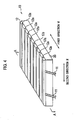
- FIG. 4 is a perspective view showing a state in which the high refractivity layer 12 is formed on the light-receiving surface of the solar cell 10.
- Fig. 5 is an enlarged sectional view of A-A section in Fig. 4 , that is, a section perpendicular to the second direction N in which the thin wire electrodes 30 extend.
- the high refractivity layer 12 has first notches 12a formed along the thin wire electrodes 30 (not shown in Fig. 4 . See Fig. 3 .) that are formed on the light-receiving surface of the photoelectric conversion part 20.
- the high refractivity layer 12 has the eight first notches 12a in the second direction N.
- each first notch 12a is formed of a pair of first tilted surfaces 12S and 12S.
- the pair of the first tilted surfaces 12S and 12S is provided on the thin wire electrode 30.
- Each of the first tilted surfaces 12S and 12S in the pair tilts to the light-receiving surface of the photoelectric conversion part 20.
- the pair of the first tilted surfaces 12S and 12S meet above the approximate center of the thin wire electrode 30.
- each first notch 12a is formed so that the notch 12a gradually deepens toward the thin wire electrode 30.
- the first notch 12a is formed so that the section thereof perpendicular to the second direction N has an inverted triangle shape (V-shape) having a vertex right above the approximate center of the thin wire electrode 30 in the first direction M.
- V-shape inverted triangle shape
- each first notch 12a is filled with the sealing member 4.
- the sealing member 4 is in contact with a pair of the first tilted surfaces 12S and 12S of the high refractivity layer 12.
- the width ⁇ of the first notch 12a is smaller than the width ⁇ of the thin wire electrode 30, the width ⁇ of the first notch 12a may be substantially equal to or larger than the width ⁇ of the thin wire electrode 30.
- the multiple solar cells 10 are connected to each other by the wiring members 11.
- a high refractivity material of thermosetting type is applied onto the light-receiving surface of each solar cell 10.
- the applied high refractivity material is cured by being heated while pressing a top panel that has convex portions corresponding to the thin wire electrodes 30, against the high refractivity material.
- each high refractivity layer 12 having pairs of the first tilted surfaces 12S and 12S are formed.
- the solar cell module 100 includes the high refractivity layer 12 being formed on the light-receiving surface of the photoelectric conversion part 20 and having a refractive index higher than that of the sealing member 4.
- the high refractive layer 12 has pairs of the first tilted surfaces 12S and 12S each being provided above the thin wire electrode 30 (collecting electrode) and having pairs of the first tilted surfaces 12S and 12S tilted relative to the light-receiving surface.
- sunlight beams incident toward each thin wire electrode 30 are refracted at the pair of the first tilted surfaces 12S and 12S, and thereby can be directed to an area of the light-receiving surface of the photoelectric conversion part 20 where no thin wire electrode 30 is formed.
- sunlight beams passing through the front surface protection member 2 and being incident toward the thin wire electrode 30 through the sealing member 4 are refracted at the pair of the first tilted surfaces 12S and 12S.
- the refracted sunlight beams are directed to the area of the light-receiving surface of the photoelectric conversion part 20 where no thin wire electrode 30 is formed.
- the high refractivity layer 12 has a refractive index higher than that of sealing member 4, an output angle ⁇ 2 can be made smaller than an incident angle ⁇ 1. Consequently, sunlight beams incident on the pair of the first tilted surfaces 12S and 12S can be efficiently directed to an effective light receiving area of the light-receiving surface of the photoelectric conversion part 20.
- the photoelectric conversion part 20 can absorb sunlight beams incident toward the thin wire electrodes 30.
- a second embodiment of the present invention will be described hereinafter with reference to the drawings.
- This embodiment differs from the first embodiment described above in that high refractivity layers 12 according to this embodiment further include second notches 12b. Since this embodiment is similar to the first embodiment described above in other points, the differences will be mainly described hereinafter with reference to Fig. 1 to Fig. 3 .
- Fig. 7 is a perspective view schematically showing a state in which the high refractivity layer 12 is formed on the light-receiving surface of the solar cell 10.
- Fig. 8 is an enlarged sectional view of a section B-B in Fig. 7 , i.e., of a section perpendicular to the first direction M in which the wiring members 11 extend.
- the high refractivity layer 12 As shown in Fig. 7 , the high refractivity layer 12 according to this embodiment has second notches 12b that are formed along the wiring members 11 (See Fig. 3 .) placed on the photoelectric conversion part 20. In this embodiment, since two wiring members 11 are placed on the photoelectric conversion part 20 in the first direction M, the high refractivity layer 12 has two second notches 12b in the first direction M.
- each second notch 12b is formed by a pair of second tilted surfaces 12T and 12T.
- the pair of the second tilted surfaces 12T and 12T is provided on the thin wire electrode 30.
- Each of the paired second tilted surfaces 12T and 12T is tilted relative to the light-receiving surface of the photoelectric conversion part 20.
- the pair of the second tilted surfaces 12T and 12 meet above the approximate center of the wiring member 11.
- each second notch 12b is formed so that the notch 12b gradually deepens toward the wiring member 11.
- the second notch 12b is formed so that the section perpendicular to the first direction M has an inverted triangle shape (V-shape) having a vertex at the approximate center of the wiring member 11 in the second direction N.
- V-shape inverted triangle shape
- each second notch 12b is filled with the sealing member 4.
- the sealing member 4 is in contact with a pair of the second tilted surfaces 12T and 12T of the high refractivity layer 12.
- the width of the second notches 12b is substantially equal to that of the wiring members 11; however, the width may be formed larger than the width of the wiring members 11.
- first notch 12a is similar to that of the first embodiment described above.
- the first notch 12a and the second notches 12b are formed so that they intersect like a grid in the plane view of the high refractivity layer 12.
- the multiple solar cells 10 are connected to each other by the wiring members 11.
- a high refractivity material of thermosetting type is applied onto the light-receiving surface of each solar cell 10.
- the applied high refractivity material is cured by being heated while pressing a top panel that has convex portions corresponding to the thin wire electrodes 30 and the wiring members 11, against the high refractivity material.
- each high refractivity layer 12 having pairs of the first tilted surfaces 12S and 12S and pairs of second tilted surfaces 12T and 12T are formed.
- the solar cell module 100 includes the high refractivity layers 12 each being provided on the light-receiving surface of the photoelectric conversion part 20 and having a refractive index higher than that of the sealing member 4.
- the high refractive layer 12 has pairs of the second tilted surfaces 12T and 12T each being provided above the wiring member 11 and tilted relative to the light-receiving surface.
- sunlight beams incident toward each wiring member 11 are refracted at the pair of the second tilted surfaces 12T and 12T, and thereby can be directed to an area of the light-receiving surface of the photoelectric conversion part 20 where no wiring member 11 is formed.
- sunlight beams passing through the front surface protection member 2 and being incident toward the wiring members 11 through the sealing member 4 are refracted at the pair of the second tilted surfaces 12T and 12T.
- the refracted sunlight beams are directed to the area of the light-receiving surface of the photoelectric conversion part 20 where no wiring member 11 is formed.
- the high refractivity layer 12 has a refractive index higher than the sealing member 4, an output angle ⁇ 2 can be made smaller than an incident angle ⁇ 1. Consequently, sunlight beams incident on the pair of the second tilted surfaces 12T and 12T can be efficiently directed to an effective light receiving area of the light-receiving surface of the photoelectric conversion part 20.
- the photoelectric conversion part 20 can absorb sunlight beams incident toward the wiring member 11.
- the pair of the first tilted surfaces 12S and 12S can direct sunlight beams incident toward the thin wire electrodes 30 to the area where no thin wire electrode 30 is formed.
- a third embodiment of the present invention will be described hereinafter with reference to the drawings.
- This embodiment differs from the first embodiment described above in that a separately formed high refractivity layer 12 is placed on the light-receiving surface of each solar cell 10. Since this embodiment is similar to the first embodiment described above in other points, the differences will be mainly described hereinafter.
- Fig. 10 is an enlarged side view of a solar cell module 100 according to this embodiment. As shown in Fig. 10 , a high refractivity layer 12 according to this embodiment is bonded onto the light-receiving surface of the solar cell 10 with a bonding member 13.
- the high refractivity layer 12 is a structure formed separately from the solar cell 10.
- the high refractivity layer 12 has the first notches 12a of the first embodiment described above.
- a bonding member 13 is a resin for bonding the high refractivity layer 12 onto the light-receiving surface of the solar cell 10.
- a translucent resin such as an EVA resin can be used as the bonding member 13.
- a high refractivity material of thermosetting type is injected into a mold that has been molded according to the shape of the high refractivity layer 12. Then, the high refractivity material in the mold is cured by heating the mold. As a result, the high refractivity layer 12 is formed.
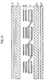
- a laminated body is formed by sequentially stacking a PET sheet (a back surface protection member 3), an EVA sheet (the sealing member 4), a solar cell string 1, EVA sheets (the bonding members 13), the high refractivity layers 12, an EVA sheet (the sealing member 4), and a glass plate (a front surface protection member 2).
- the laminated body is heated and pressure bonded in a vacuum atmosphere.
- the EVA is softened and then filled into the first notch 12a.
- the EVA is cured. Accordingly, the solar cell module 100 is manufactured.
- Each high refractivity layer 12 is formed as a structure separate from the solar cell 10. Thus, after the solar cell string 1 is formed, it is no longer necessary to form the high refractivity layers on respective light-receiving surfaces of the multiple solar cells 10. In other words, separately preparing the high refractivity layer 12 enables modularization of the high refractivity layer 12 together with other members. Consequently, the manufacturing processes can be simplified.
- sunlight beams incident toward the thin wire electrodes 30 can be directed by the first notch 12a to the area where no thin wire electrode 30 is formed, similarly to the first embodiment described above.
- the high refractivity layer 12 is formed to cover the substantially whole light-receiving surface of the photoelectric conversion part 20.
- the high refractivity layer 12 is formed along the thin wire electrodes 30.
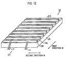
- Fig. 12 is a perspective view showing a state in which the multiple high refractivity layers 12A are formed on the light-receiving surface of the solar cell 10.
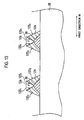
- Fig. 13 is an enlarged sectional view of a section C-C in Fig. 12 .
- a solar cell module 100 includes the multiple high refractivity layers 12A formed on the light-receiving surface of the photoelectric conversion part 20.
- Each high refractivity layer 12A has the first notch 12a.
- Each high refractivity layer 12A is provided on the thin wire electrode 30 along the thin wire electrode 30.
- the first notch 12a is formed by a pair of first tilted surfaces 12S 1 and 12S 1 .
- the pair of the first tilted surfaces 12S 1 and 12S 1 is provided above the thin wire electrode 30.
- Each of the paired first surfaces 12S 1 and 12S 1 is tilted relative to the light-receiving surface of the photoelectric conversion part 20.
- the pair of the first surfaces 12S 1 and 12S 1 each of which is formed flat, meet above the approximate center of the thin wire electrode 30.
- the high refractivity layer 12A has a pair of sides 12S 2 and 12S 2 .
- the pair of sides 12S 2 and 12S 2 are the surfaces of the high refractivity layers 12A extending from the tops of the pair of the first tilted surfaces 12S 1 and 12S 1 to the light-receiving surface of the photoelectric conversion part 20, respectively.
- the paired sides 12S 2 and 12S 2 meet and make acute angles with the paired first tilted surfaces 12S 1 and 12S 1 , respectively.
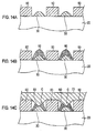
- a high refractivity material 60 of thermosetting type is applied on each thin wire electrode 30 along thereof.
- the applied high refractivity material 60 is cured by being heated while pressing a top plate 70 that has convex portions corresponding to the respective thin wire electrodes 30 against the high refractivity material 60.
- each high refractivity layer 12A having the pair of the first tilted surfaces 12S 1 and 12S 1 and the pair of the sides 12S 2 and 12S 2 .
- each high refractivity layer 12A according to this embodiment has the pair of the first tilted surfaces 12S 1 and 12S 1 , similar effects to the first embodiment described above can be achieved.
- each high refractivity layer 12A has the pair of the sides 12S 2 and 12S 2 .
- sunlight beams incident toward each thin wire electrode 30 can also be directed to an area on the light-receiving surface of the photoelectric conversion part 20 where no thin wire electrode 30 is formed, by refracting the sunlight beams at the pair of the sides 12S 2 and 12S 2 .
- each high refractivity layer 12A according to this embodiment is formed along the thin wire electrode 30.
- usage of the high refractive material is smaller than the case in which the high refractivity layer 12 is formed to cover the light-receiving surface of the photoelectric conversion part 20, manufacturing cost of the solar cell module 100 can be reduced.
- a fifth embodiment of the present invention will be described hereinafter with reference to the drawings. In the following, differences from the fourth embodiment described above will be mainly described. Specifically, in the fourth embodiment described above the high refractivity layers 12 are formed by using the masks. In contrast, high refractivity layers 12 are formed without using masks, in the fifth embodiment.
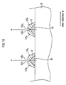
- Fig. 16 is a sectional view of the solar cell 10 for illustrating the configuration of the high refractivity layer 12B.
- the paired first tilted surfaces 12S 1 and 12S 1 are gently curved and then meet the paired sides 12S 2 and 12S 2 , respectively.
- the paired first tilted surfaces 12S 1 and 12S 1 and the paired sides 12S 2 and 12S 2 form curved surfaces.
- a high refractivity material 60 is applied symmetrically relative to a center line P of each thin wire electrode 30.
- the height of the high refractivity material 60 to be applied can be adjusted by adjusting scanning speed of a dispenser device or viscosity of the high refractivity material 60.
- each high refractivity layer 12B having the pair of the first tilted surfaces 12S 1 and 12S 1 and the pair of the sides 12S 2 and 12S 2 .
- each high refractivity layer 12B according to the embodiment has the pair of the tilted surfaces 12S 1 and 12S 1 and the pair of the sides 12S 2 and 12S 2 , the effects similar to those of the fourth embodiment described above can be achieved.
- the high refractivity layer 12B according to the embodiment is formed without using masks, by means of the dispenser method.
- the manufacturing processes of the solar cell module 100 can be simplified, compared with the case in which the high refractivity layers are formed by using the masks.
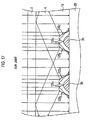
- the paired first tilted surfaces 12S 1 and 12S 1 and the paired sides 12S 2 and 12S 2 gently meet, respectively, and form the curved surfaces.
- an incident angle to the front surface protection member 2 of incident light reflected at the surface of the high refractivity layer 12B can be made larger.
- reflectivity at an interface between the front surface protection member 2 and the sealing member 4 can be increased. Consequently, the electric generating capacity of the solar cell module 100 can be further improved.
- the high refractivity layer 12 has the pair of the first tilted surfaces 12 and 12S 1 and the pair of the sides 12S 2 and 12S 2 .
- a high refractivity layer 12 has one first tilted surface 12S 1 and one side 12S 2 in the sixth embodiment.
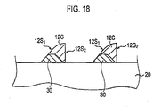
- Fig. 18 is a sectional view of the solar cell 10 for illustrating the configuration of the high refractivity layer 12C.
- the high refractivity layer 12C has one first tilted surface 12S 1 and one side 12S 2 .
- the first tilted surface 12S 1 covers one side of the surface of the thin wire electrode 30.
- the side 12S 2 is formed substantially perpendicular to the light-receiving surface of the photoelectric conversion part 20 on the light-receiving surface.
- the first tilted surface 12S 1 is formed to gradually diminish from the top of the side 12S 2 to the surface of the thin wire electrode 30, and convexly curved toward the front surface protection member 2.
- masks 50 are applied so that all thin wire electrodes 30 are exposed on the light-receiving surface of the photoelectric conversion part 20.
- a high refractivity material 60 of thermosetting type is applied so as to cover one side the surface of each thin wire electrode 30.
- the high refractivity material 60 applied on the masks 50 is removed with the masks 50. Then, the remaining high refractivity material 60 is heated and cured. As a result, the high refractivity layer 12C having the one first tilted surface 12S 1 and the one side 12S 2 is formed.
- each high refractivity layer 12C according to this embodiment has the one first tilted surface 12S 1 and the one side 12S 2 , the same effects as those of the first and fourth embodiments can be achieved as shown in Fig. 20A .
- the same effects as those of the first and fourth embodiments can be achieved as shown in Fig. 20A .
- the thin wire electrode 30 since one end of the thin wire electrode 30 is tilted although it is exposed, light incident on the one end is easy to direct to the light-receiving surface.
- the one first tilted surface 12S 1 is formed to gradually diminish from the top of the side 12S 2 to the surface of the thin wire electrode 30, and thus convexly curved toward the front surface protection member 2.
- the incident light can be directed to the light-receiving surface efficiently.
- the shape like the high refractivity layer 12C can makes it easy to design the shape, which thereby can further improve the reflection efficiency of the incident light.
- the shape of the thin wire electrode 30 is not limited to this.
- the thin wire electrode 30 may also be formed on the wave line, or the multiple thin wire electrodes 30 may intersect like a grid.
- the wiring members 11 are soldered onto the connecting electrodes 40, the wiring members 11 may be bonded onto the photoelectric conversion part 20 with a resin adhesive.
- sides of the notches may not be planar shaped.
- the sides of the notches may be curved in consideration of the refractive index of the high refractivity layer 12.
- the multiple thin wire electrodes 30 are formed on the back surface of the photoelectric conversion part 20, the multiple thin wire electrodes may be formed to cover the whole back surface.
- the present invention should not limit the shape of the thin wire electrodes 30 to be formed on the back surface of the photoelectric conversion part 20.
- the pair of the sides 12S 2 and 12S 2 are tilted to the light-receiving surface in the fourth embodiment described above, they may also be formed to be perpendicular to the light-receiving surface.
- Embodiments of a solar cell module according to the present invention will be specifically described hereinafter. However, the present invention should not be limited to those shown in the following embodiments, but may be modified appropriately and implemented within a scope that does not change the gist thereof.
- photoelectric conversion parts were each fabricated using an n-type single crystal silicon substrate that is 100 mm square. Then, by a screen printing method, thin wire electrodes and connecting electrodes are formed like a grid on a light-receiving surface and a back surface of each photoelectric conversion part by use of a silver paste of epoxy thermosetting type.
- flattened wiring members are each solder connected with a connecting electrode formed on the light-receiving surface of one solar cell and a connecting electrode formed on the back surface of another solar cell adjacent to the one solar cell.
- a solar cell string was fabricated by repeating this.
- fluorene acrylate which is a macromolecule polymer of thermosetting type, was applied onto the light-receiving surface of the solar cell.
- fluorene acrylate was cured by heating it at 150°C while pressing a top plate that has convex portions corresponding to positions of the thin wire electrodes.
- a high refractivity layer having first notches was formed.
- the refractive index of the high refractivity layer was 1.63.
- the solar cell module according to Example 1 was manufactured by sealing the solar cell string placed between a glass and a PET film, in an EVA.
- Example 2 differs from Example 1 described above in a configuration of the high refractivity layer.
- a solar cell string was fabricated, similarly to Example 1. Then, polyimide was applied to a light-receiving surface of each solar cell. Next, the polyimide was cured by being heated at 200°C while pressing a top plate that has convex portions corresponding to positions of thin wire electrodes and wiring members against the polyimide. As a result, the high refractivity layer having the first notches and second notches was formed. Additionally, the refractive index of the high refractivity layer was 1.7.
- the solar cell module according to Example 2 was manufactured by sealing the solar cell string placed between a glass and a PET film in an EVA.
- Example 3 differs from Example 1 described above in a configuration of the high refractivity layer.
- a solar cell string was fabricated, similarly to the Example 1. Then, an episulfide resin was injected into a mold that has been molded according to the shape of the high refractivity layer. Then, after the episulfide resin was polymerized by being heated at 80°C, the polymerized episulfide resin was annealed at 120°C. As a result, each high refractivity layer having first notches was formed. Additionally, the refractive index of the high refractivity layer was 1.73.
- the solar cell module according to the Example 3 was manufactured by sequentially stacking a PET film, EVA, the solar cell string, EVA, high refractivity layers, EVA, and a glass, and then heating the laminated body to pressure bonding these components.
- Comparative Example differs from Example 1 described above in that the solar cell module according to Comparative Example includes no high refractivity layer. Thus, no high refractivity material was applied onto the light-receiving surface of each solar cell. Any other processes are similar to those in Example 1 described above.
- Example 1 The value of short-circuit current in Example 1 was improved by 3.2% relative to that in Comparative Example. This is because light incident toward each thin wire electrode was directed to the photoelectric conversion part by refracting the light by the high refractivity layer having first notches.
- Example 2 the value of short-circuit current in Example 2 was improved by 4.0% relative to that in Comparative Example. This is because light incident toward each of the thin wire electrodes and wiring members was directed to the photoelectric conversion part by refracting the light by the high refractivity layer having the first notches and second notches. The value of short-circuit current in Example 2 was improved more than that in Example 1, because the light incident toward each wiring member was utilized for photoelectric conversion.
- Example 3 the value of short-circuit current in Example 3 was improved by 3.3% relative to that in Comparative Example. This is because light incident toward each thin wire electrode was directed to the photoelectric conversion part by refracting the light by the high refractivity layer having the first notches. Thus, it was found that the effect similar to those in Example 1 is achieved even when the high refractivity layer was fabricated as a separate structure.
Landscapes
- Photovoltaic Devices (AREA)
Applications Claiming Priority (2)
| Application Number | Priority Date | Filing Date | Title |
|---|---|---|---|
| JP2008021864 | 2008-01-31 | ||
| JP2008324046A JP2009206494A (ja) | 2008-01-31 | 2008-12-19 | 太陽電池モジュール |
Publications (2)
| Publication Number | Publication Date |
|---|---|
| EP2086016A2 true EP2086016A2 (de) | 2009-08-05 |
| EP2086016A3 EP2086016A3 (de) | 2012-04-04 |
Family
ID=40720008
Family Applications (1)
| Application Number | Title | Priority Date | Filing Date |
|---|---|---|---|
| EP09250254A Withdrawn EP2086016A3 (de) | 2008-01-31 | 2009-01-30 | Solarzellenmodul |
Country Status (5)
| Country | Link |
|---|---|
| US (1) | US20090194148A1 (de) |
| EP (1) | EP2086016A3 (de) |
| JP (1) | JP2009206494A (de) |
| KR (1) | KR20090084740A (de) |
| CN (1) | CN101521241B (de) |
Cited By (1)
| Publication number | Priority date | Publication date | Assignee | Title |
|---|---|---|---|---|
| EP2595200A3 (de) * | 2011-11-18 | 2017-03-22 | Shin-Etsu Chemical Co., Ltd. | Solarzellenmodul und Lichtsteuerblatt für ein Solarzellenmodul |
Families Citing this family (14)
| Publication number | Priority date | Publication date | Assignee | Title |
|---|---|---|---|---|
| JP5558339B2 (ja) * | 2010-12-28 | 2014-07-23 | 京セラ株式会社 | 光電変換モジュールの製造方法 |
| KR101151759B1 (ko) * | 2011-05-16 | 2012-06-15 | 정 욱 한 | 학습교구용 태양전지 모듈 |
| KR101265929B1 (ko) * | 2011-10-21 | 2013-05-20 | 류한희 | 태양전지의 상부 표면 처리 방법 및 그에 따라 제조된 태양전지 |
| KR101985053B1 (ko) * | 2012-03-27 | 2019-05-31 | 쓰리엠 이노베이티브 프로퍼티즈 컴파니 | 광 지향 매체를 포함하는 광기전 모듈 및 이를 제조하는 방법 |
| WO2013176319A1 (ko) * | 2012-05-24 | 2013-11-28 | Jeong Yeong Sik | 학습교구용 태양전지 모듈 |
| TWI482305B (zh) * | 2012-09-27 | 2015-04-21 | Win Win Prec Technology Co Ltd | 太陽能電池模組及其製造方法、提升太陽能電池元件散熱效果的方法以及散熱增強型太陽能電池元件 |
| TWM461152U (zh) * | 2013-05-13 | 2013-09-01 | Win Win Prec Technology Co Ltd | 太陽能電池模組 |
| WO2017066146A1 (en) | 2015-10-12 | 2017-04-20 | 3M Innovative Properties Company | Light redirecting film useful with solar modules |
| KR102705764B1 (ko) * | 2017-02-22 | 2024-09-12 | 오와이 아이씨에스 인텔리전트 컨트롤 시스템즈 리미티드 | 광전지용 광학 실드 |
| CN108389926A (zh) * | 2018-01-18 | 2018-08-10 | 合肥晶澳太阳能科技有限公司 | 一种光伏组件的封装方法 |
| JP2020098902A (ja) * | 2018-12-14 | 2020-06-25 | パナソニック株式会社 | 太陽電池モジュール |
| DE202023102281U1 (de) * | 2023-01-16 | 2023-06-02 | Jinko Solar Co., Ltd. | Photovoltaikmodul |
| US12581749B2 (en) | 2023-01-16 | 2026-03-17 | Zhejiang Jinko Solar Co., Ltd. | Photovoltaic module and method for manufacturing photovoltaic module |
| CN120936144B (zh) * | 2025-10-16 | 2025-12-26 | 天合光能股份有限公司 | 太阳能电池和太阳能电池的制备方法 |
Citations (2)
| Publication number | Priority date | Publication date | Assignee | Title |
|---|---|---|---|---|
| JPH0671093B2 (ja) | 1985-04-19 | 1994-09-07 | 株式会社日立製作所 | 光発電素子 |
| JP2006040937A (ja) | 2004-07-22 | 2006-02-09 | Canon Inc | 太陽電池およびその製造方法 |
Family Cites Families (21)
| Publication number | Priority date | Publication date | Assignee | Title |
|---|---|---|---|---|
| US534498A (en) * | 1895-02-19 | descamps | ||
| US4053327A (en) * | 1975-09-24 | 1977-10-11 | Communications Satellite Corporation | Light concentrating solar cell cover |
| US4311869A (en) * | 1978-06-30 | 1982-01-19 | Exxon Research & Engineering Co. | Solar cell modules |
| US4379202A (en) * | 1981-06-26 | 1983-04-05 | Mobil Solar Energy Corporation | Solar cells |
| JPS62248182A (ja) * | 1986-04-22 | 1987-10-29 | Matsushita Graphic Commun Syst Inc | デイスクカ−トリツジ |
| US4749430A (en) * | 1986-10-16 | 1988-06-07 | Shell Oil Company | Method of making an encapsulated assemblage |
| JPH02504496A (ja) * | 1988-06-03 | 1990-12-20 | シエル・インターナシヨナル・リサーチ・マートスハツペイ・ベー・ヴエー | 封入集合体及びその製造方法 |
| US5110370A (en) * | 1990-09-20 | 1992-05-05 | United Solar Systems Corporation | Photovoltaic device with decreased gridline shading and method for its manufacture |
| JP2938634B2 (ja) * | 1991-10-08 | 1999-08-23 | キヤノン株式会社 | 太陽電池モジュール |
| JPH06104473A (ja) * | 1992-09-22 | 1994-04-15 | Oki Electric Ind Co Ltd | 太陽光を利用した発電装置 |
| JP3078933B2 (ja) * | 1992-12-28 | 2000-08-21 | キヤノン株式会社 | 光起電力装置 |
| US5554229A (en) * | 1995-02-21 | 1996-09-10 | United Solar Systems Corporation | Light directing element for photovoltaic device and method of manufacture |
| JPH10233519A (ja) * | 1996-01-10 | 1998-09-02 | Canon Inc | 太陽電池モジュール |
| US6072692A (en) * | 1998-10-08 | 2000-06-06 | Asahi Glass Company, Ltd. | Electric double layer capacitor having an electrode bonded to a current collector via a carbon type conductive adhesive layer |
| JP2001094126A (ja) * | 1999-09-20 | 2001-04-06 | Kanegafuchi Chem Ind Co Ltd | 太陽電池モジュール |
| JP2001168365A (ja) * | 1999-09-27 | 2001-06-22 | Kanegafuchi Chem Ind Co Ltd | 太陽電池モジュール |
| JP2004111742A (ja) * | 2002-09-19 | 2004-04-08 | Sharp Corp | 太陽電池 |
| JP2005099693A (ja) * | 2003-09-05 | 2005-04-14 | Hitachi Chem Co Ltd | 反射防止膜形成用組成物及びそれを用いた反射防止膜の製造方法、光学部品、太陽電池ユニット |
| JP2005285948A (ja) * | 2004-03-29 | 2005-10-13 | Sharp Corp | 太陽電池モジュールおよびその製造方法 |
| JP2006041168A (ja) * | 2004-07-27 | 2006-02-09 | Canon Inc | 太陽電池モジュール及び太陽電池モジュールの製造方法 |
| CN101014890B (zh) * | 2004-09-08 | 2011-01-19 | 东丽株式会社 | 光布线用树脂组合物和光电复合布线基板 |
-
2008
- 2008-12-19 JP JP2008324046A patent/JP2009206494A/ja active Pending
-
2009
- 2009-01-30 EP EP09250254A patent/EP2086016A3/de not_active Withdrawn
- 2009-01-30 US US12/362,641 patent/US20090194148A1/en not_active Abandoned
- 2009-01-30 KR KR1020090007413A patent/KR20090084740A/ko not_active Ceased
- 2009-02-01 CN CN2009100051356A patent/CN101521241B/zh not_active Expired - Fee Related
Patent Citations (2)
| Publication number | Priority date | Publication date | Assignee | Title |
|---|---|---|---|---|
| JPH0671093B2 (ja) | 1985-04-19 | 1994-09-07 | 株式会社日立製作所 | 光発電素子 |
| JP2006040937A (ja) | 2004-07-22 | 2006-02-09 | Canon Inc | 太陽電池およびその製造方法 |
Cited By (1)
| Publication number | Priority date | Publication date | Assignee | Title |
|---|---|---|---|---|
| EP2595200A3 (de) * | 2011-11-18 | 2017-03-22 | Shin-Etsu Chemical Co., Ltd. | Solarzellenmodul und Lichtsteuerblatt für ein Solarzellenmodul |
Also Published As
| Publication number | Publication date |
|---|---|
| US20090194148A1 (en) | 2009-08-06 |
| CN101521241A (zh) | 2009-09-02 |
| EP2086016A3 (de) | 2012-04-04 |
| CN101521241B (zh) | 2012-07-18 |
| JP2009206494A (ja) | 2009-09-10 |
| KR20090084740A (ko) | 2009-08-05 |
Similar Documents
| Publication | Publication Date | Title |
|---|---|---|
| EP2086016A2 (de) | Solarzellenmodul | |
| EP3731282B1 (de) | Solarbatteriemodul | |
| CN103339735B (zh) | 太阳能电池及太阳能电池模块 | |
| JP5484663B2 (ja) | 太陽電池モジュールの製造方法 | |
| JP5842170B2 (ja) | 太陽電池モジュール | |
| US10879410B2 (en) | Solar cell module | |
| JP6526774B2 (ja) | 太陽電池モジュール | |
| CN108475706B (zh) | 太阳能电池模块 | |
| EP2234167A2 (de) | Solarzelle und Solarzellenmodul | |
| JP7270631B2 (ja) | 太陽電池モジュール | |
| WO2012164814A1 (ja) | 太陽電池モジュール | |
| JP5436805B2 (ja) | 太陽電池モジュール | |
| JP2018046112A (ja) | 太陽電池モジュール | |
| US20090293934A1 (en) | Photoelectric Conversion Device | |
| US10784392B2 (en) | Solar cell module and method for manufacturing the same | |
| US20200035847A1 (en) | Solar cell module | |
| TWI613407B (zh) | 具波浪狀之光伏模組及其製法 | |
| JP2018056490A (ja) | 太陽電池モジュールおよび太陽電池セル | |
| CN121310720B (zh) | 间隙膜及光伏组件 | |
| JP7606859B2 (ja) | 太陽電池セル、太陽電池モジュール及び太陽電池セル製造方法 | |
| KR20140121915A (ko) | 양면 수광형 태양전지 모듈 | |
| JP2017135244A (ja) | 太陽電池モジュールおよび太陽光発電システム |
Legal Events
| Date | Code | Title | Description |
|---|---|---|---|
| PUAI | Public reference made under article 153(3) epc to a published international application that has entered the european phase |
Free format text: ORIGINAL CODE: 0009012 |
|
| AK | Designated contracting states |
Kind code of ref document: A2 Designated state(s): AT BE BG CH CY CZ DE DK EE ES FI FR GB GR HR HU IE IS IT LI LT LU LV MC MK MT NL NO PL PT RO SE SI SK TR |
|
| AX | Request for extension of the european patent |
Extension state: AL BA RS |
|
| PUAL | Search report despatched |
Free format text: ORIGINAL CODE: 0009013 |
|
| AK | Designated contracting states |
Kind code of ref document: A3 Designated state(s): AT BE BG CH CY CZ DE DK EE ES FI FR GB GR HR HU IE IS IT LI LT LU LV MC MK MT NL NO PL PT RO SE SI SK TR |
|
| AX | Request for extension of the european patent |
Extension state: AL BA RS |
|
| RIC1 | Information provided on ipc code assigned before grant |
Ipc: H01L 31/048 20060101ALI20120228BHEP Ipc: H01L 31/052 20060101ALI20120228BHEP Ipc: H01L 31/0232 20060101AFI20120228BHEP |
|
| 17P | Request for examination filed |
Effective date: 20121003 |
|
| AKX | Designation fees paid |
Designated state(s): DE ES FR IT |
|
| 17Q | First examination report despatched |
Effective date: 20130624 |
|
| STAA | Information on the status of an ep patent application or granted ep patent |
Free format text: STATUS: THE APPLICATION IS DEEMED TO BE WITHDRAWN |
|
| 18D | Application deemed to be withdrawn |
Effective date: 20131105 |