EP2086032A2 - Dispositifs électroluminescents organiques - Google Patents
Dispositifs électroluminescents organiques Download PDFInfo
- Publication number
- EP2086032A2 EP2086032A2 EP08020968A EP08020968A EP2086032A2 EP 2086032 A2 EP2086032 A2 EP 2086032A2 EP 08020968 A EP08020968 A EP 08020968A EP 08020968 A EP08020968 A EP 08020968A EP 2086032 A2 EP2086032 A2 EP 2086032A2
- Authority
- EP
- European Patent Office
- Prior art keywords
- light emitting
- organic light
- layer
- emitting device
- emitting layer
- Prior art date
- Legal status (The legal status is an assumption and is not a legal conclusion. Google has not performed a legal analysis and makes no representation as to the accuracy of the status listed.)
- Granted
Links
- 0 Cc1cc(*[C@@]2*=CC=CC2)ccc1 Chemical compound Cc1cc(*[C@@]2*=CC=CC2)ccc1 0.000 description 3
Images


Classifications
-
- H—ELECTRICITY
- H10—SEMICONDUCTOR DEVICES; ELECTRIC SOLID-STATE DEVICES NOT OTHERWISE PROVIDED FOR
- H10K—ORGANIC ELECTRIC SOLID-STATE DEVICES
- H10K50/00—Organic light-emitting devices
- H10K50/10—OLEDs or polymer light-emitting diodes [PLED]
- H10K50/11—OLEDs or polymer light-emitting diodes [PLED] characterised by the electroluminescent [EL] layers
- H10K50/125—OLEDs or polymer light-emitting diodes [PLED] characterised by the electroluminescent [EL] layers specially adapted for multicolour light emission, e.g. for emitting white light
-
- C—CHEMISTRY; METALLURGY
- C09—DYES; PAINTS; POLISHES; NATURAL RESINS; ADHESIVES; COMPOSITIONS NOT OTHERWISE PROVIDED FOR; APPLICATIONS OF MATERIALS NOT OTHERWISE PROVIDED FOR
- C09K—MATERIALS FOR MISCELLANEOUS APPLICATIONS, NOT PROVIDED FOR ELSEWHERE
- C09K11/00—Luminescent materials, e.g. electroluminescent or chemiluminescent
- C09K11/02—Use of particular materials as binders, particle coatings or suspension media therefor
- C09K11/025—Use of particular materials as binders, particle coatings or suspension media therefor non-luminescent particle coatings or suspension media
-
- C—CHEMISTRY; METALLURGY
- C09—DYES; PAINTS; POLISHES; NATURAL RESINS; ADHESIVES; COMPOSITIONS NOT OTHERWISE PROVIDED FOR; APPLICATIONS OF MATERIALS NOT OTHERWISE PROVIDED FOR
- C09K—MATERIALS FOR MISCELLANEOUS APPLICATIONS, NOT PROVIDED FOR ELSEWHERE
- C09K11/00—Luminescent materials, e.g. electroluminescent or chemiluminescent
- C09K11/06—Luminescent materials, e.g. electroluminescent or chemiluminescent containing organic luminescent materials
-
- H—ELECTRICITY
- H10—SEMICONDUCTOR DEVICES; ELECTRIC SOLID-STATE DEVICES NOT OTHERWISE PROVIDED FOR
- H10K—ORGANIC ELECTRIC SOLID-STATE DEVICES
- H10K50/00—Organic light-emitting devices
- H10K50/10—OLEDs or polymer light-emitting diodes [PLED]
- H10K50/11—OLEDs or polymer light-emitting diodes [PLED] characterised by the electroluminescent [EL] layers
- H10K50/12—OLEDs or polymer light-emitting diodes [PLED] characterised by the electroluminescent [EL] layers comprising dopants
-
- H—ELECTRICITY
- H10—SEMICONDUCTOR DEVICES; ELECTRIC SOLID-STATE DEVICES NOT OTHERWISE PROVIDED FOR
- H10K—ORGANIC ELECTRIC SOLID-STATE DEVICES
- H10K50/00—Organic light-emitting devices
- H10K50/10—OLEDs or polymer light-emitting diodes [PLED]
- H10K50/19—Tandem OLEDs
-
- H—ELECTRICITY
- H10—SEMICONDUCTOR DEVICES; ELECTRIC SOLID-STATE DEVICES NOT OTHERWISE PROVIDED FOR
- H10K—ORGANIC ELECTRIC SOLID-STATE DEVICES
- H10K85/00—Organic materials used in the body or electrodes of devices covered by this subclass
- H10K85/30—Coordination compounds
- H10K85/321—Metal complexes comprising a group IIIA element, e.g. Tris (8-hydroxyquinoline) gallium [Gaq3]
- H10K85/324—Metal complexes comprising a group IIIA element, e.g. Tris (8-hydroxyquinoline) gallium [Gaq3] comprising aluminium, e.g. Alq3
-
- H—ELECTRICITY
- H10—SEMICONDUCTOR DEVICES; ELECTRIC SOLID-STATE DEVICES NOT OTHERWISE PROVIDED FOR
- H10K—ORGANIC ELECTRIC SOLID-STATE DEVICES
- H10K85/00—Organic materials used in the body or electrodes of devices covered by this subclass
- H10K85/60—Organic compounds having low molecular weight
- H10K85/615—Polycyclic condensed aromatic hydrocarbons, e.g. anthracene
- H10K85/626—Polycyclic condensed aromatic hydrocarbons, e.g. anthracene containing more than one polycyclic condensed aromatic rings, e.g. bis-anthracene
-
- H—ELECTRICITY
- H10—SEMICONDUCTOR DEVICES; ELECTRIC SOLID-STATE DEVICES NOT OTHERWISE PROVIDED FOR
- H10K—ORGANIC ELECTRIC SOLID-STATE DEVICES
- H10K85/00—Organic materials used in the body or electrodes of devices covered by this subclass
- H10K85/60—Organic compounds having low molecular weight
- H10K85/631—Amine compounds having at least two aryl rest on at least one amine-nitrogen atom, e.g. triphenylamine
-
- H—ELECTRICITY
- H10—SEMICONDUCTOR DEVICES; ELECTRIC SOLID-STATE DEVICES NOT OTHERWISE PROVIDED FOR
- H10K—ORGANIC ELECTRIC SOLID-STATE DEVICES
- H10K85/00—Organic materials used in the body or electrodes of devices covered by this subclass
- H10K85/60—Organic compounds having low molecular weight
- H10K85/631—Amine compounds having at least two aryl rest on at least one amine-nitrogen atom, e.g. triphenylamine
- H10K85/633—Amine compounds having at least two aryl rest on at least one amine-nitrogen atom, e.g. triphenylamine comprising polycyclic condensed aromatic hydrocarbons as substituents on the nitrogen atom
-
- H—ELECTRICITY
- H10—SEMICONDUCTOR DEVICES; ELECTRIC SOLID-STATE DEVICES NOT OTHERWISE PROVIDED FOR
- H10K—ORGANIC ELECTRIC SOLID-STATE DEVICES
- H10K85/00—Organic materials used in the body or electrodes of devices covered by this subclass
- H10K85/60—Organic compounds having low molecular weight
- H10K85/649—Aromatic compounds comprising a hetero atom
- H10K85/657—Polycyclic condensed heteroaromatic hydrocarbons
- H10K85/6572—Polycyclic condensed heteroaromatic hydrocarbons comprising only nitrogen in the heteroaromatic polycondensed ring system, e.g. phenanthroline or carbazole
-
- C—CHEMISTRY; METALLURGY
- C09—DYES; PAINTS; POLISHES; NATURAL RESINS; ADHESIVES; COMPOSITIONS NOT OTHERWISE PROVIDED FOR; APPLICATIONS OF MATERIALS NOT OTHERWISE PROVIDED FOR
- C09K—MATERIALS FOR MISCELLANEOUS APPLICATIONS, NOT PROVIDED FOR ELSEWHERE
- C09K2211/00—Chemical nature of organic luminescent or tenebrescent compounds
- C09K2211/10—Non-macromolecular compounds
- C09K2211/1003—Carbocyclic compounds
- C09K2211/1011—Condensed systems
-
- C—CHEMISTRY; METALLURGY
- C09—DYES; PAINTS; POLISHES; NATURAL RESINS; ADHESIVES; COMPOSITIONS NOT OTHERWISE PROVIDED FOR; APPLICATIONS OF MATERIALS NOT OTHERWISE PROVIDED FOR
- C09K—MATERIALS FOR MISCELLANEOUS APPLICATIONS, NOT PROVIDED FOR ELSEWHERE
- C09K2211/00—Chemical nature of organic luminescent or tenebrescent compounds
- C09K2211/10—Non-macromolecular compounds
- C09K2211/1003—Carbocyclic compounds
- C09K2211/1014—Carbocyclic compounds bridged by heteroatoms, e.g. N, P, Si or B
-
- H—ELECTRICITY
- H10—SEMICONDUCTOR DEVICES; ELECTRIC SOLID-STATE DEVICES NOT OTHERWISE PROVIDED FOR
- H10K—ORGANIC ELECTRIC SOLID-STATE DEVICES
- H10K2101/00—Properties of the organic materials covered by group H10K85/00
- H10K2101/90—Multiple hosts in the emissive layer
-
- H—ELECTRICITY
- H10—SEMICONDUCTOR DEVICES; ELECTRIC SOLID-STATE DEVICES NOT OTHERWISE PROVIDED FOR
- H10K—ORGANIC ELECTRIC SOLID-STATE DEVICES
- H10K50/00—Organic light-emitting devices
- H10K50/10—OLEDs or polymer light-emitting diodes [PLED]
- H10K50/11—OLEDs or polymer light-emitting diodes [PLED] characterised by the electroluminescent [EL] layers
- H10K50/12—OLEDs or polymer light-emitting diodes [PLED] characterised by the electroluminescent [EL] layers comprising dopants
- H10K50/121—OLEDs or polymer light-emitting diodes [PLED] characterised by the electroluminescent [EL] layers comprising dopants for assisting energy transfer, e.g. sensitization
-
- H—ELECTRICITY
- H10—SEMICONDUCTOR DEVICES; ELECTRIC SOLID-STATE DEVICES NOT OTHERWISE PROVIDED FOR
- H10K—ORGANIC ELECTRIC SOLID-STATE DEVICES
- H10K50/00—Organic light-emitting devices
- H10K50/10—OLEDs or polymer light-emitting diodes [PLED]
- H10K50/11—OLEDs or polymer light-emitting diodes [PLED] characterised by the electroluminescent [EL] layers
- H10K50/125—OLEDs or polymer light-emitting diodes [PLED] characterised by the electroluminescent [EL] layers specially adapted for multicolour light emission, e.g. for emitting white light
- H10K50/13—OLEDs or polymer light-emitting diodes [PLED] characterised by the electroluminescent [EL] layers specially adapted for multicolour light emission, e.g. for emitting white light comprising stacked EL layers within one EL unit
-
- H—ELECTRICITY
- H10—SEMICONDUCTOR DEVICES; ELECTRIC SOLID-STATE DEVICES NOT OTHERWISE PROVIDED FOR
- H10K—ORGANIC ELECTRIC SOLID-STATE DEVICES
- H10K50/00—Organic light-emitting devices
- H10K50/10—OLEDs or polymer light-emitting diodes [PLED]
- H10K50/14—Carrier transporting layers
- H10K50/15—Hole transporting layers
-
- H—ELECTRICITY
- H10—SEMICONDUCTOR DEVICES; ELECTRIC SOLID-STATE DEVICES NOT OTHERWISE PROVIDED FOR
- H10K—ORGANIC ELECTRIC SOLID-STATE DEVICES
- H10K50/00—Organic light-emitting devices
- H10K50/10—OLEDs or polymer light-emitting diodes [PLED]
- H10K50/14—Carrier transporting layers
- H10K50/16—Electron transporting layers
-
- H—ELECTRICITY
- H10—SEMICONDUCTOR DEVICES; ELECTRIC SOLID-STATE DEVICES NOT OTHERWISE PROVIDED FOR
- H10K—ORGANIC ELECTRIC SOLID-STATE DEVICES
- H10K71/00—Manufacture or treatment specially adapted for the organic devices covered by this subclass
- H10K71/831—Aging
-
- Y—GENERAL TAGGING OF NEW TECHNOLOGICAL DEVELOPMENTS; GENERAL TAGGING OF CROSS-SECTIONAL TECHNOLOGIES SPANNING OVER SEVERAL SECTIONS OF THE IPC; TECHNICAL SUBJECTS COVERED BY FORMER USPC CROSS-REFERENCE ART COLLECTIONS [XRACs] AND DIGESTS
- Y02—TECHNOLOGIES OR APPLICATIONS FOR MITIGATION OR ADAPTATION AGAINST CLIMATE CHANGE
- Y02B—CLIMATE CHANGE MITIGATION TECHNOLOGIES RELATED TO BUILDINGS, e.g. HOUSING, HOUSE APPLIANCES OR RELATED END-USER APPLICATIONS
- Y02B20/00—Energy efficient lighting technologies, e.g. halogen lamps or gas discharge lamps
Definitions
- the present invention relates to organic light emitting devices, and more particularly, to monochromatic organic light emitting devices for improving the lifetime markedly, and further relates to white organic light emitting devices for improving the lifetime markedly.
- Organic light emitting devices have attracted a lot of interests because of the advantages such as thin, large-plane, solid-state and flexible, wherein white organic light emitting devices have become focus due to demonstrated applications in the solid-state light source or as backlight for liquid crystal displays.
- OLED organic light emitting device
- OLEDs The high efficiency, high luminescent intensity and color stability of OLEDs are particularly significant to their industrializations.
- phosphorescent materials are introduced to OLEDs which result in that the triplet and singlet excitons are fully used, and so that the luminescent intensity and efficiency are improved markedly.
- the lifetime of blue devices and blue emitting layer of devices is the key problem combining the characteristics of OLEDs, and ways of developing long-lifetime blue materials and optimizing the structures of OLEDs are used to improve the lifetime.
- the Chinese patent document 200510007765.9 and 200510007786.0 of sanyo disclosed a device where the lifetime was improved through introducing two kinds of dopants
- the Chinese patent document 01120883.X of Eastman Kodak disclosed a device where the lifetime was as well improved by introducing the first dopant which could accept election-hole energy from host and the second dopant which could accept energy from hole of host.
- the doped luminescent layers above are all doped in shingle luminescent layer, and the disadvantage is the low efficiency.
- the compound monochromatic luminescent layer includes cither of blue emitting layer, green emitting layer, red emitting layer, or yellow emitting layer.
- the hole transporting material includes triarylamine, carbazole derivatives and pyrazolin derivatives.
- the electron-transporting material includes anthracene, oxadiazole derivative, metal chelates and conjugated polycyclic aromatic compounds.
- one of the host A and the dopant thereof are the same as the host B and the dopant thereof.
- the host A can be a single material with both the hole-transporting characteristic and the electron-transporting characteristic, such as CBP, and the chemical structure of CBP as follows:
- the host A doped with monochromatic dopant could be adulterated with auxiliary materials, and the auxiliary material could be another monochromatic dopant.
- the monochromatic luminescent layer is blue emitting layer
- the chemical structure of the blue dopant is represented by the following formula 8-(13):
- the organic electroluminescent medium includes one or more of hole-injection layer, hole-transporting layer, electron-injection layer and electron-transporting layer.
- a white organic light emitting device comprising:
- the host A includes two kinds of materials with different transporting characteristics, one is hole-transporting material, and the other is electron-transporting material.
- the compound monochromatic luminescent layer includes either of the blue emitting layer, green emitting layer, red emitting layer, or yellow emitting layer.
- the hole-transporting material includes triarylamine, carbazole derivatives and pyrazolin derivatives.
- the electron-transporting material includes anthracene, oxadiazole derivative, metal chelates and conjugated polycyclic aromatic; compounds.
- one of the host A and the dopant thereof are the same as the host B and the dopant thereof.
- the host A can be a single material with both the hole-transporting characteristic and the electron-transporting characteristic, such as CBP, the chemical structure of CBP in (14).
- organic electroluminescent medium includes compound blue emitting layer, green emitting layer and red emitting layer.
- organic electroluminescent medium includes compound blue emitting layer and yellow emitting layer.
- organic electroluminescent medium includes compound green emitting layer, blue emitting layer and red emitting layer.
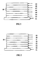
- Example 1 A blue light emitting device is reported in Example 1 and the device structure is shown in Fig 1 , wherein the luminescent layer 09 is compound blue emitting layer containing two layers 06 and 07.
- the blue emitting layer 1(06) contains host A doped with blue dopant where the host A is funned by two kinds of materials with different transporting characteristics, one of which is electron-transporting material represented by the following formula 4(BH1 for short):
- the formula of the blue dopant is 8 (BD1 for short):
- the blue emitting layer 2(07) is formed by a host D and a blue dopant, where the host B is electron-transporting material and the blue dopant is BD1, and the device has the following device structure: ITO / NPB / BH ⁇ 1 : NPB : BD ⁇ 1 / BH ⁇ 1 : BD ⁇ 1 / Alq 3 / LiF / Al
- the device of device structure (1) is fabricated by the following procedures successively:
- the device has the following device structure: ITO / NPB / BHl : BD ⁇ 1 / Alq 3 / LiF / Al
- the device of device structure (2) is fabricated by the following procedures successively:
- the device has the following device structure: ITO / NPB / BH ⁇ 1 : NPB : BD ⁇ 1 / ALq 3 / LiF / Al
- the device of device structure (3) is fabricated by the following procedures successively:
- Table 1 exhibits the characteristics of these devices of Example 1 and Comparative example 1 and 2, and the corresponding graphs are shown in Fig 5 .
- Table 1 Devices Device structure of the luminescent layer Lifetime at the same initial lamina nce(h) Efficiency (cd/A)
- Example 1 BH1:20%NPB:5%BD1(10nm)/BH1:5%BD1(1 5nm) 428 5.9
- Comparative example 1 BH1:20%NPB:5%BD1(25nm) 132 4.5
- Example 1 the device lifetime of Example 1 is improved markedly compared to that of Comparative example 1 wherein the device has only blue luminescent layer 1 with host A, and Comparative example 2 wherein the device has only blue luminescent layer 2 with host B. Additionally, the efficiency of Example 1 is not decreased so much as higher than the devices with only blue luminescent layer 1 or 2.
- the device has the following device structure: ITO / NPB / BH ⁇ 1 : NPB X % : BD ⁇ 1 Ynm / BH ⁇ 1 : BD ⁇ 1 / Alq 3 / LiF / Al
- the device of device structure (4) is fabricated by the following procedures successively:
- Table 2 exhibits the characteristics of these devices with different weight ratio and thickness of Example 2.
- Table 2 Device structure of the luminescent layer Xwt% Y(nm) Lifetime (h) Efficiency (cd/A) BH1:NPB(20%):BD1(3%)(10nm)/BH1:BD1 20 10 500 6 BH1:NPB(40%):BD1(3%)(10nm)/Bm;BD1 40 10 200 5.6 BH1:NPB(600%):BD1(3%)(10nm)/BH1:BD1 60 10 200 4 BH1:NPB(20%):BD1(3%)(20nm)/BH1:BD1 20 20 250 5 BH1:NTB(40%):BD1(3%)(20nm)/BH1:HD1 40 20 200 4.5 BH1:NPB(60%):BD1(3%)(20nm)/BH1:BD1 60 20 150 3.5
- the longest lifetime is obtained at the following condition: the weight ratio of NPB and BD1 to BH1 is 20% and 3% respectively, and the layer thickness of the blue light emitting layer 1 is 10nm.
- the marked lifetime improvement of the device having compound blue luminescent layer according to the above examples and comparative examples may be attributed to the following reasons:
- the unrecombined holes enter the electron transporting layer Alq 3 , they will form the unstable Alq 3 cationic species that will decrease the stability of the device.
- the blue luminescent layer 2 is inserted between the Alq 3 layer and the blue luminescent layer 1 and the holes could be blocked and consumed by recombination in the blue light emitting layer 2. There are fewer holes to inject into Alq 3 , which prevents the formation of Alq 3 *, so the stability and efficiency was enhanced.
- the introducing of the host A caused the enhancement of vitrification temperature.
- vitrification temperature is low generally, however, that was enhanced because of the doping with other materials in the blue luminescent layer 1, which improved the heat stability of the whole device.
- Example 3 Another blue light emitting device using different blue material is reported in Example 3, and the device structure , same as Example 1, is showed in Fig 1 .
- the devices also employ compound luminescent layer, wherein the electron-transporting material of blue luminescent layer 1 makes use of BAlq, and the hole-transporting material makes use of NPB, while blue dopant is TBPe.
- the BAlq and TBPe are also used in blue luminescent layer 2 as host and dopant respectively.
- the device has the following device structure: ITO / NPB / BAlq : NPB : TBPe / BAlq : TBPe / Alq 3 / LiF / Al
- the device of device structure (5) is fabricated by the procedure similar to Example 1
- the device has the following device structure: ITO / NPB / BAlq : TBPe / Alq 3 / LiF / Al
- the device of device structure (6) is fabricated by the following procedures successively:
- the device has the following device structure: ITO / NPB / BAlq : NPB : TBPe / Alq 3 / LiF / Al
- the device of device structure (7) is fabricated by the following procedures successively:
- Table 3 exhibits the characteristics of these devices of Example 3 and Comparative example 3 and 4, and the corresponding graphs are shown in Fig 6 .
- Table 3 Devices Device structure of the luminescent layer Lifetime at the same initial luminance(h) Efficiency (cd/A)
- Example 3 BAlq:20%NPB:3%TBPe(10nm)/BAlq:3%TBPe(15 nm) 125 43
- Comparative example 3 BAlq:3%TBPe(25nm) 16.3
- Comparative example 4 BAlq:20%NPB:3%TBPe(25nm) 35 2.3
- Example 3 It can be seen from Table 3 and Fig 6 that the device lifetime of example 3 is improved markedly compared to that of Comparative example 3 and 4. Additionally, the efficiency of Example 3 is not decreased.
- a green light emitting device is reported in Example 4 and the device structure is shown in Fig 2 , wherein the luminescent layer 09 is compound green emitting layer containing two layers :layer 10 and layer 11.
- the green emitting layer 1(10) contains host A doped with green dopant where the host A is formed by two kinds of materials with different transporting characteristics, one of which is electron-transporting material BAlq, the other is hole-transporting material NPB, and the green dopant is C545T,
- the green emitting layer 2(11) is formed by a host B and a green dopant, where the host B is electron-transporting material BAlq and the green dopant is C545T, and the device has the following device structure: ITO / NPB / BAlq : NPB : C ⁇ 545 ⁇ T / BAlq : C ⁇ 545 ⁇ T / Alq 3 / LiF / Al
- the device of device structure (8) is fabricated by the procedure similar to Example 1.
- the device has the following device structure: ITO / NPB / BAlq : C ⁇ 545 ⁇ T / Alq 3 / LiF / Al
- the device of device structure (9) is fabricated by the following procedures successively:
- the device has the following device structure: ITO / NPB / BAlq : NPB : C ⁇ 545 ⁇ T / Alq 3 / LiF / Al
- the device of device structure (10) is fabricated by the following procedures successively:
- Table 4 exhibits the characteristics of these devices of Example 4 and Comparative example 5 and 6, and the corresponding graphs are shown in Fig 7 .
- Example 4 BAlq:20%NPB:2%C545T(10nm)/BAlq: 2%C545T (15nm) 895 10.1 Comparative example 5 BAlq:2%C545T(25nm) 118 10.5 Comparative example 6 BAlq:20%NPB:2%C545T(25nm) 252 8.1
- Example 4 It can be seen from Table 4 and Fig 7 that the device lifetime of Example: 4 is improved markedly compared to that of Comparative example 5 and 6. Additionally, the efficiency of Example 4 is not decreased.
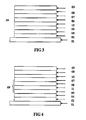
- Example 5 A white organic light emitting device with two luminescent centers is reported in Example 5 and the device structure is shown in Fig 3 , wherein the luminescent layer 09 includes yellow emitting layer 12 and compound blue emitting layer containing two layers :blue emitting layer 1(06) and blue emitting layer 2(07).
- the yellow emitting layer 12 is formed by hole-transporting material NPB and yellow dopant (such as rubrene).
- the blue emitting layer 2(07) includes electron-transporting material BH1 and blue dopant BD1
- the blue emitting layer 1(06) includes host A doped with green dopant where the host A is formed by two kinds of materials with different transporting characteristics, one of which is electron-transporting material BH1, the other is hole-transporting material NPB.
- the preferable device has the following device structure: ITO / NPB / NPB : rubrene / BH ⁇ 1 : NPB : BD ⁇ 1 / BH ⁇ 1 : BD ⁇ 1 / Alq 3 / LiF / Al
- the white organic light emitting device of device structure (11) is fabricated by the following procedures successively:
- the device has the following device structure: ITO / NPB / NPB : rubrene / BH ⁇ 1 : BD ⁇ 1 / Alq 3 / LiF / Al
- the white organic light emitting device of device structure (12) is fabricated by the following procedures successively:
- the device has the following device structure: ITO / NPB / NPB : rubrene / BH ⁇ 1 : NPB : BD ⁇ 1 / Alq 3 / LiF / Al
- the white organic light emitting device of device structure (13) is fabricated by the following procedures successively:
- Table 5 exhibits the characteristics of these devices of Example 5 and Comparative example 7 and 8, and the corresponding graphs are shown in Fig 8 .
- Example 5 NPB:rubrene/BH1:20%NPB:3%BD1(10 mn)/BH1.3%BD1(20nm) 312 10 White
- Comparative example 7 NPB:rubrene/BH1:3%BDI(20nm) 66 10.3 White on the yellow side
- Comparative example 8 NPB:rubrene/BH1:20%NPB:3%BD1(20 nm) 142 8.3 White
- the device has the following device structure: ITO / NPB / NPB : DCM / BAlq : NPB X % : TBPe Ynm / BAlq : TBPe / Alq 3 / LiF / Al
- the white organic light emitting device of device structure (14) is fabricated by the following procedures successively:
- Table 6 exhibits the characteristics of these devices with different weight ratio and thickness of Example 6.
- Table 6 Device structure of the compound blue emitting layer Xwt % Y(nm) Lifetime (h) Efficiency (cd/A) Color BAlq:NPB(20%):TBPe(3%)(10nm)/BA1 q:TBPe 20 10 803 8 White BAlq:NPB(40%):TBPe(3%)(10nm)/BAI q:TBPe 40 10 507 7.5 White BAlq:NPB(60%):TBPe(3%)(10nm)/BAl q:TBPe 60 10 411 6 White on the blue side BAlq:NPB(20%):TBPe(3%)(20nm)/DAl q:TBPe 20 20 453 7 White BAlq:NPB(40%):TBPe(3%)(20nm)/BAl q:TBPe 40 20 387 6.5 White BAlq:NPB(60%):TBP
- Example 7 Another white organic light emitting device with three luminescent centers is reported in Example 7 and the device structure is shown in Fig 4 , wherein the luminescent layer 09 includes green emitting layer 11, compound blue luminescent layer containing the blue emitting layer 1(06) and the blue emitting layer 2(07), and the red emitting layer 13.
- the luminescent layer 09 includes green emitting layer 11, compound blue luminescent layer containing the blue emitting layer 1(06) and the blue emitting layer 2(07), and the red emitting layer 13.
- the green emitting layer 11 includes NPB as host and Ir(ppy) 3 as green dopant;
- the blue emitting layer 2(07) includes electron-transporting material BAlq as host and TBPe as blue dopant;
- the emitting layer 1(06) includes host A doped with blue dopant and the host A is formed by two kinds of materials with different transporting characteristics;
- the red emitting layer includes Alq 3 as host and DCJTB or Ir(piq) 2 (acac) as red dopant.
- the preferable device has the following device structure: ITO / NPB / NPB : C ⁇ 545 ⁇ T / BAlq : NPB : TBPe / BAlq : TBPe / Alq 3 : Ir ⁇ piq 2 acac / Alq 3 / LiF / Al
- the white organic light emitting device of device structure (15) is fabricated by the following procedures successively:
- the device has the following device structure: ITO / NPB / NPB : C ⁇ 545 ⁇ T / BAlq : TBPe / Alq 3 : Ir ⁇ piq 2 acac / Alq 3 / LiF / Al
- the white organic light emitting device of device structure (16) is fabricated by the Mowing procedures successively:
- the device has the following device structure: ITO / NPB / NPB : C ⁇ 545 ⁇ T / BAlq : NPB : TBPe / Alq 3 : Ir ⁇ piq 2 acac / Alq 3 / LiF / Al
- the device of device structure (17) is fabricated with the same procedures as above described towards device (15), except for cancelling the blue emitting layer 2.
- Table 7 exhibits the characteristics of these devices of Example 7 and Comparative example 9 and 10, and the corresponding graphs are shown in Fig 9 .
- Example 7 NPB:C545T/BAlq:20%NPB:3%TBPe(20 nm)/BAlq:3%TBPe(20nm)/Alq 3 :Ir(piq) 2 ( acac) 248 14.8
- White Comparative example 9 NPB:C545T/BAlq:3%TBPe(20nm)/Alq: Ir(piq) 2 (acac) 72 15
- Comparative example 10 NPB:C545T/BAlq:20%NPB:3%TRPe(20 nm)/Alq 3 :Ir(piq) 2 (acac) 128 11 White on the red side
- Example 7 It can be seen from Table 7 and Fig 9 that the device lifetime of Example 7 is improved markedly compared to that of Comparative example 9 and 10. Additionally, the device efficiency of Example 7 is not decreased.
- Example 8 A white organic light emitting device with two luminescent centers is reported in Example 8, wherein the luminescent layer includes yellow emitting layer, the blue emitting layer 1 and the blue emitting layer 2, wherein the blue emitting layer 1 contains a host B with both the hole-transporting characteristic and the electron-transporting characteristic.
- the preferable device has the following device structure: ITO / NPB / NPB : rubrene / CBP : TBPe / BAlq : TBPe / Alq 3 / LiF / Al
- the device of device structure (18) is fabricated with the same procedures as above described towards Example 5, except for changing the blue emitting layer 1 which contains a host B CBP.
- the deposition rate of CBP is 0.1nm/s and the weight ratio of TBPe is 3%.
- the thickness of the blue emitting layer 1 and the blue emitting layer 2 is 10nm and 20nm respectively.
- Table 8 Device structure of the luminescent layer Lifetime (h) Efficiency (cd/A) color NPB:rubrene/CBP:3%TBPe(10nm)/BAlq:3%TBPe(20um) 775 9 White MPB:rubrene/CBP:3%TBPe(20nm)/BAlq:3%TBPe(20nm) 601 7.9 White NPB:ubrene/BAlq:3%TBPe(20nm) 497 9 White NPB:rubrene/CBP:3%TBPe(10nm) 452 7.5 White on the yellow side
- the dopant of the blue emitting layer can also be either BCzVBi, BCzVB, DPAVBi, DPAVB. BDAVBi or N-BDAVBi.
- a white organic light emitting device including a compound blue emitting layer is reported in Example 9, wherein the blue emitting layer 1 and blue emitting layer 2 both contain a yellow dye.
- the blue emitting layer 1 contains host A and a blue dopant, and the host A includes an electron-transporting material and a hole-transporting material.
- the blue emitting layer 2 contains an electron-transporting material and a blue dopant.
- the preferable device has the following device structure: ITO / NPB / BH ⁇ 1 : NPB : BD ⁇ 1 : rubrene / BH ⁇ 1 : BD ⁇ 1 : rubrene / Alq 3 / LiF / Al
- the white organic light emitting device of device structure (21) is fabricated by the following procedures successively:
- Table 9 exhibits the characteristics of these devices of Example 9 and Comparative examples, and the corresponding graphs are shown in Fig 10 .
- White Comparative example 11 RH1:5%RD1:1%rubrene(25nm) 663 11.8
- White Comparative example 12 BH1:20%NPB:5%BD1:1%rubrene(25nm ) 834 9.6
- h initial luminance
- ed/A Efficiency
Landscapes
- Chemical & Material Sciences (AREA)
- Engineering & Computer Science (AREA)
- Materials Engineering (AREA)
- Physics & Mathematics (AREA)
- Spectroscopy & Molecular Physics (AREA)
- Optics & Photonics (AREA)
- Organic Chemistry (AREA)
- Inorganic Chemistry (AREA)
- Electroluminescent Light Sources (AREA)
Priority Applications (1)
| Application Number | Priority Date | Filing Date | Title |
|---|---|---|---|
| PL08020968T PL2086032T3 (pl) | 2008-01-29 | 2008-12-03 | Organiczne urządzenia emitujące światło |
Applications Claiming Priority (1)
| Application Number | Priority Date | Filing Date | Title |
|---|---|---|---|
| CNB2008100570160A CN100484353C (zh) | 2008-01-29 | 2008-01-29 | 有机电致发光器件 |
Publications (3)
| Publication Number | Publication Date |
|---|---|
| EP2086032A2 true EP2086032A2 (fr) | 2009-08-05 |
| EP2086032A3 EP2086032A3 (fr) | 2011-05-18 |
| EP2086032B1 EP2086032B1 (fr) | 2017-10-18 |
Family
ID=39921012
Family Applications (1)
| Application Number | Title | Priority Date | Filing Date |
|---|---|---|---|
| EP08020968.7A Active EP2086032B1 (fr) | 2008-01-29 | 2008-12-03 | Dispositifs électroluminescents organiques |
Country Status (6)
| Country | Link |
|---|---|
| US (2) | US9196856B2 (fr) |
| EP (1) | EP2086032B1 (fr) |
| JP (1) | JP5231188B2 (fr) |
| KR (1) | KR101026514B1 (fr) |
| CN (1) | CN100484353C (fr) |
| PL (1) | PL2086032T3 (fr) |
Cited By (4)
| Publication number | Priority date | Publication date | Assignee | Title |
|---|---|---|---|---|
| EP2494620A4 (fr) * | 2009-10-29 | 2013-11-06 | Du Pont | Panneaux lumineux à diodes électroluminescentes organiques |
| US8716700B2 (en) | 2009-10-29 | 2014-05-06 | E I Du Pont De Nemours And Company | Organic light-emitting diodes having white light emission |
| WO2018206138A1 (fr) * | 2017-05-08 | 2018-11-15 | Cynora Gmbh | Dispositif électroluminescent organique |
| US10403839B2 (en) | 2011-02-16 | 2019-09-03 | Semiconductor Energy Laboratory Co., Ltd. | Light-emitting element |
Families Citing this family (34)
| Publication number | Priority date | Publication date | Assignee | Title |
|---|---|---|---|---|
| EP2294641A4 (fr) * | 2008-06-26 | 2012-08-08 | Du Pont | Luminaires à diodes électroluminescentes organiques |
| KR101750301B1 (ko) | 2009-05-29 | 2017-06-23 | 가부시키가이샤 한도오따이 에네루기 켄큐쇼 | 발광 소자, 발광 장치, 전자기기 및 조명 장치 |
| JP2013502701A (ja) * | 2009-08-24 | 2013-01-24 | イー・アイ・デュポン・ドウ・ヌムール・アンド・カンパニー | 有機発光ダイオード照明器具 |
| US8476620B2 (en) * | 2009-08-24 | 2013-07-02 | E I Du Pont De Nemours And Company | Organic light-emitting diode luminaires |
| EP2471121A4 (fr) * | 2009-08-24 | 2013-10-30 | Du Pont | Luminaires à diodes électroluminescentes organiques |
| TW201121117A (en) * | 2009-08-24 | 2011-06-16 | Du Pont | Organic light-emitting diode luminaires |
| CN102484217A (zh) * | 2009-08-24 | 2012-05-30 | E.I.内穆尔杜邦公司 | 有机发光二极管灯具 |
| EP2471120A2 (fr) * | 2009-08-24 | 2012-07-04 | E. I. du Pont de Nemours and Company | Luminaires à diodes électroluminescentes organiques |
| US20110260603A1 (en) * | 2009-10-29 | 2011-10-27 | E.I. Du Pont De Nemours And Company | Organic light-emitting diode luminaires |
| KR101657222B1 (ko) * | 2010-05-14 | 2016-09-19 | 삼성디스플레이 주식회사 | 유기 발광 소자 |
| CN102082232A (zh) * | 2010-09-16 | 2011-06-01 | 昆山维信诺显示技术有限公司 | 一种蓝光有机电致发光器件 |
| CN102969455B (zh) * | 2012-12-18 | 2015-08-05 | 中国科学院长春应用化学研究所 | 白色有机电致发光器件及其制备方法 |
| TWI556486B (zh) * | 2012-12-20 | 2016-11-01 | 財團法人工業技術研究院 | 白光有機發光二極體 |
| EP2941473B1 (fr) * | 2013-01-03 | 2018-01-31 | Merck Patent GmbH | Dispositif électronique |
| CN103500802A (zh) * | 2013-10-12 | 2014-01-08 | 京东方科技集团股份有限公司 | 有机电致发光器件 |
| CN103762317B (zh) * | 2013-12-30 | 2016-08-17 | 昆山工研院新型平板显示技术中心有限公司 | 一种有机电致发光器件 |
| JP2015201279A (ja) * | 2014-04-04 | 2015-11-12 | セイコーエプソン株式会社 | 発光素子、発光装置、表示装置および電子機器 |
| US9929365B2 (en) * | 2014-05-28 | 2018-03-27 | The Regents Of The University Of Michigan | Excited state management |
| US10749118B2 (en) | 2014-06-26 | 2020-08-18 | Samsung Display Co., Ltd. | Heterocyclic compound and organic light-emitting device including the same |
| CN104795507B (zh) * | 2015-04-16 | 2017-03-22 | 京东方科技集团股份有限公司 | 有机电致发光器件及其制造方法、电子设备 |
| US10290816B2 (en) | 2015-11-16 | 2019-05-14 | The Regents Of The University Of Michigan | Organic electroluminescent materials and devices |
| CN105609653A (zh) * | 2016-03-09 | 2016-05-25 | 苏州大学 | 一种白光oled器件及其制备方法 |
| CN105679957B (zh) * | 2016-04-20 | 2017-12-05 | 京东方科技集团股份有限公司 | 有机发光器件及其制备方法 |
| CN106024844B (zh) * | 2016-07-27 | 2019-01-22 | 京东方科技集团股份有限公司 | 有机发光器件及其制备方法、显示装置 |
| CN106328818B (zh) * | 2016-08-26 | 2018-11-20 | 深圳市华星光电技术有限公司 | 荧光/磷光混合型白光有机发光二极管 |
| KR102673970B1 (ko) * | 2016-10-13 | 2024-06-11 | 삼성디스플레이 주식회사 | 유기발광 표시장치 그 제조방법 |
| CN108565346B (zh) * | 2018-04-16 | 2020-08-14 | 山西大同大学 | 一种双色全荧光白光oled器件 |
| CN110577545B (zh) * | 2018-06-07 | 2021-04-16 | 江苏三月科技股份有限公司 | 一种三芳胺类化合物及其在有机电致发光器件上的应用 |
| KR102721590B1 (ko) * | 2018-08-17 | 2024-10-23 | 엘지디스플레이 주식회사 | 유기전계발광소자 |
| CN110544748A (zh) * | 2019-08-09 | 2019-12-06 | 合肥工业大学 | 一种提升热延迟荧光oled器件效率的方法 |
| CN110993810A (zh) * | 2019-12-24 | 2020-04-10 | 吉林奥来德光电材料股份有限公司 | 一种有机电致发光器件 |
| CN111864088A (zh) * | 2020-07-06 | 2020-10-30 | 武汉华星光电半导体显示技术有限公司 | 一种有机发光二极管器件及其显示面板 |
| CN113113455A (zh) * | 2021-03-31 | 2021-07-13 | 武汉华星光电半导体显示技术有限公司 | Oled显示面板与显示装置 |
| CN114373874A (zh) * | 2021-11-30 | 2022-04-19 | 合肥福纳科技有限公司 | 量子点电致发光器件及其制备方法 |
Citations (6)
| Publication number | Priority date | Publication date | Assignee | Title |
|---|---|---|---|---|
| US20050147844A1 (en) | 2004-01-05 | 2005-07-07 | Eastman Kodak Company | White oled devices with color filter arrays |
| US20050221121A1 (en) | 2004-03-31 | 2005-10-06 | Hitachi Displays, Ltd. | Organic light-emitting element, image display device and production method thereof |
| US20060003184A1 (en) | 2004-07-01 | 2006-01-05 | Eastman Kodak Company | High performance white light-emitting OLED device |
| US20060040132A1 (en) | 2004-08-20 | 2006-02-23 | Eastman Kodak Company | White OLED having multiple white electroluminescence units |
| US20070099026A1 (en) | 2005-07-15 | 2007-05-03 | Samsung Sdi Co., Ltd. | White organic light emitting diode and method for manufacturing the same |
| US20070228938A1 (en) | 2006-03-30 | 2007-10-04 | Eastman Kodak Company | Efficient white-light OLED display with filters |
Family Cites Families (23)
| Publication number | Priority date | Publication date | Assignee | Title |
|---|---|---|---|---|
| CN1120883A (zh) | 1994-10-19 | 1996-04-24 | 邓友银 | 六杆分插秧机构 |
| JP2001338761A (ja) | 2000-05-26 | 2001-12-07 | Toyota Motor Corp | 有機el素子 |
| US6475648B1 (en) | 2000-06-08 | 2002-11-05 | Eastman Kodak Company | Organic electroluminescent devices with improved stability and efficiency |
| JP4287198B2 (ja) | 2002-11-18 | 2009-07-01 | 出光興産株式会社 | 有機エレクトロルミネッセンス素子 |
| US6967062B2 (en) | 2003-03-19 | 2005-11-22 | Eastman Kodak Company | White light-emitting OLED device having a blue light-emitting layer doped with an electron-transporting or a hole-transporting material or both |
| JP4651918B2 (ja) | 2003-05-21 | 2011-03-16 | 東北パイオニア株式会社 | 有機elパネルの製造方法 |
| US7045952B2 (en) * | 2004-03-04 | 2006-05-16 | Universal Display Corporation | OLEDs with mixed host emissive layer |
| JP2005285470A (ja) | 2004-03-29 | 2005-10-13 | Sanyo Electric Co Ltd | 有機エレクトロルミネッセンス素子 |
| JP2005293992A (ja) | 2004-03-31 | 2005-10-20 | Sanyo Electric Co Ltd | 有機エレクトロルミネッセンス素子の製造方法 |
| US8951645B2 (en) * | 2004-04-09 | 2015-02-10 | Lg Chem, Ltd. | Stacked organic light emitting device having high efficiency and high brightness |
| TWI382079B (zh) * | 2004-07-30 | 2013-01-11 | Sanyo Electric Co | 有機電場發光元件及有機電場發光顯示裝置 |
| CN1791289A (zh) | 2004-12-14 | 2006-06-21 | 胜华科技股份有限公司 | 有机发光元件 |
| CN101115708B (zh) * | 2005-02-07 | 2010-10-13 | 出光兴产株式会社 | 芳香族胺衍生物以及使用其的有机电致发光元件 |
| US20060194076A1 (en) * | 2005-02-28 | 2006-08-31 | Fuji Photo Film Co., Ltd. | Organic electroluminescent element |
| US7421348B2 (en) | 2005-03-18 | 2008-09-02 | Swanson Brian G | Predictive emissions monitoring method |
| JP2007042875A (ja) | 2005-08-03 | 2007-02-15 | Fujifilm Holdings Corp | 有機電界発光素子 |
| US7839078B2 (en) | 2005-09-15 | 2010-11-23 | Fujifilm Corporation | Organic electroluminescent element having a luminescent layer and a buffer layer adjacent thereto |
| US20070100179A1 (en) * | 2005-10-28 | 2007-05-03 | Chun-Liang Lai | Novel compounds for an organic electroluminescent device and an organic electroluminescent device comprising said compounds |
| US7718276B2 (en) * | 2006-07-18 | 2010-05-18 | Global Oled Technology Llc | Light emitting device containing phosphorescent complex |
| US20080061685A1 (en) * | 2006-08-24 | 2008-03-13 | Chesterfield Reid J | Organic electronic devices |
| KR100862068B1 (ko) | 2007-03-29 | 2008-10-09 | 단국대학교 산학협력단 | 단일 청색 호스트에 선택적 도핑 기법을 적용한 백색유기발광소자 |
| US8420229B2 (en) * | 2007-10-26 | 2013-04-16 | Global OLED Technologies LLC | OLED device with certain fluoranthene light-emitting dopants |
| KR100924145B1 (ko) * | 2008-06-10 | 2009-10-28 | 삼성모바일디스플레이주식회사 | 유기전계발광소자 및 이의 제조방법 |
-
2008
- 2008-01-29 CN CNB2008100570160A patent/CN100484353C/zh active Active
- 2008-11-27 JP JP2008303096A patent/JP5231188B2/ja active Active
- 2008-12-03 EP EP08020968.7A patent/EP2086032B1/fr active Active
- 2008-12-03 PL PL08020968T patent/PL2086032T3/pl unknown
- 2008-12-03 US US12/327,365 patent/US9196856B2/en active Active
- 2008-12-22 KR KR1020080131595A patent/KR101026514B1/ko active Active
-
2015
- 2015-10-19 US US14/886,282 patent/US10026904B2/en active Active
Patent Citations (6)
| Publication number | Priority date | Publication date | Assignee | Title |
|---|---|---|---|---|
| US20050147844A1 (en) | 2004-01-05 | 2005-07-07 | Eastman Kodak Company | White oled devices with color filter arrays |
| US20050221121A1 (en) | 2004-03-31 | 2005-10-06 | Hitachi Displays, Ltd. | Organic light-emitting element, image display device and production method thereof |
| US20060003184A1 (en) | 2004-07-01 | 2006-01-05 | Eastman Kodak Company | High performance white light-emitting OLED device |
| US20060040132A1 (en) | 2004-08-20 | 2006-02-23 | Eastman Kodak Company | White OLED having multiple white electroluminescence units |
| US20070099026A1 (en) | 2005-07-15 | 2007-05-03 | Samsung Sdi Co., Ltd. | White organic light emitting diode and method for manufacturing the same |
| US20070228938A1 (en) | 2006-03-30 | 2007-10-04 | Eastman Kodak Company | Efficient white-light OLED display with filters |
Cited By (11)
| Publication number | Priority date | Publication date | Assignee | Title |
|---|---|---|---|---|
| EP2494620A4 (fr) * | 2009-10-29 | 2013-11-06 | Du Pont | Panneaux lumineux à diodes électroluminescentes organiques |
| US8674343B2 (en) | 2009-10-29 | 2014-03-18 | E I Du Pont De Nemours And Company | Organic light-emitting diodes having white light emission |
| US8716700B2 (en) | 2009-10-29 | 2014-05-06 | E I Du Pont De Nemours And Company | Organic light-emitting diodes having white light emission |
| US10403839B2 (en) | 2011-02-16 | 2019-09-03 | Semiconductor Energy Laboratory Co., Ltd. | Light-emitting element |
| US11038135B2 (en) | 2011-02-16 | 2021-06-15 | Semiconductor Energy Laboratory Co., Ltd. | Light-emitting element |
| US11812626B2 (en) | 2011-02-16 | 2023-11-07 | Semiconductor Energy Laboratory Co., Ltd. | Light-emitting element |
| US12150325B2 (en) | 2011-02-16 | 2024-11-19 | Semiconductor Energy Laboratory Co., Ltd. | Light-emitting element |
| WO2018206138A1 (fr) * | 2017-05-08 | 2018-11-15 | Cynora Gmbh | Dispositif électroluminescent organique |
| CN110832659A (zh) * | 2017-05-08 | 2020-02-21 | 赛诺拉有限公司 | 有机电致发光器件 |
| CN110832659B (zh) * | 2017-05-08 | 2022-10-11 | 三星显示有限公司 | 有机电致发光器件 |
| EP4250899A3 (fr) * | 2017-05-08 | 2023-11-08 | Samsung Display Co., Ltd. | Dispositif électroluminescent organique |
Also Published As
| Publication number | Publication date |
|---|---|
| CN101237731A (zh) | 2008-08-06 |
| PL2086032T3 (pl) | 2018-05-30 |
| US10026904B2 (en) | 2018-07-17 |
| US20090189509A1 (en) | 2009-07-30 |
| JP5231188B2 (ja) | 2013-07-10 |
| CN100484353C (zh) | 2009-04-29 |
| KR101026514B1 (ko) | 2011-04-01 |
| EP2086032A3 (fr) | 2011-05-18 |
| US9196856B2 (en) | 2015-11-24 |
| EP2086032B1 (fr) | 2017-10-18 |
| JP2009182322A (ja) | 2009-08-13 |
| US20160043324A1 (en) | 2016-02-11 |
| KR20090083275A (ko) | 2009-08-03 |
Similar Documents
| Publication | Publication Date | Title |
|---|---|---|
| EP2086032A2 (fr) | Dispositifs électroluminescents organiques | |
| CN101340749B (zh) | 有机发光装置 | |
| KR100712290B1 (ko) | 유기전계발광소자 | |
| EP1986473B1 (fr) | Dispositif électroluminescent organique | |
| US9142791B2 (en) | OLED having multi-component emissive layer | |
| US8304097B2 (en) | White organic light emitting device | |
| KR101407574B1 (ko) | 백색 유기 발광 소자 | |
| US8866377B2 (en) | Long lifetime phosphorescent organic light emitting device (OLED) structures | |
| CN101005119B (zh) | 有机发光器件以及包括该有机发光器件的平板显示器 | |
| US8778511B2 (en) | OLED stability via doped hole transport layer | |
| CN113228334B (zh) | 有机发光器件,其制造方法,以及用于其中的组合物 | |
| KR20150046900A (ko) | 유기전계발광소자 | |
| KR20090050369A (ko) | 유기 발광 소자 | |
| KR20100072644A (ko) | 유기전계발광소자 | |
| CN100471352C (zh) | 一种有机电致发光器件 | |
| KR20160040352A (ko) | 유기발광표시장치 및 그 제조방법 | |
| US20080074047A1 (en) | Tandem organic electroluminescent element and display use of the same | |
| KR20090131550A (ko) | 유기 발광 소자 | |
| CN101030625A (zh) | 一种有机电致发光器件 | |
| CN101163359A (zh) | 一种有机电致发光器件 | |
| KR100622229B1 (ko) | 플러렌계 탄소화합물을 이용한 발광 표시장치 및 그의 제조방법 | |
| CN101510588B (zh) | 一种有机电致发光器件 | |
| Zeng et al. | 24.5: High‐Performance Electron‐Blocking Layer Materials for OLED | |
| KR20210077366A (ko) | 유기발광 다이오드 및 이를 포함하는 표시장치 | |
| CN112467046A (zh) | 一种有机电致发光器件及其制备方法和显示装置 |
Legal Events
| Date | Code | Title | Description |
|---|---|---|---|
| PUAI | Public reference made under article 153(3) epc to a published international application that has entered the european phase |
Free format text: ORIGINAL CODE: 0009012 |
|
| AK | Designated contracting states |
Kind code of ref document: A2 Designated state(s): AT BE BG CH CY CZ DE DK EE ES FI FR GB GR HR HU IE IS IT LI LT LU LV MC MT NL NO PL PT RO SE SI SK TR |
|
| AX | Request for extension of the european patent |
Extension state: AL BA MK RS |
|
| PUAL | Search report despatched |
Free format text: ORIGINAL CODE: 0009013 |
|
| AK | Designated contracting states |
Kind code of ref document: A3 Designated state(s): AT BE BG CH CY CZ DE DK EE ES FI FR GB GR HR HU IE IS IT LI LT LU LV MC MT NL NO PL PT RO SE SI SK TR |
|
| AX | Request for extension of the european patent |
Extension state: AL BA MK RS |
|
| 17P | Request for examination filed |
Effective date: 20110810 |
|
| AKX | Designation fees paid |
Designated state(s): AT BE BG CH CY CZ DE DK EE ES FI FR GB GR HR HU IE IS IT LI LT LU LV MC MT NL NO PL PT RO SE SI SK TR |
|
| 17Q | First examination report despatched |
Effective date: 20130122 |
|
| REG | Reference to a national code |
Ref country code: DE Ref legal event code: R079 Ref document number: 602008052519 Country of ref document: DE Free format text: PREVIOUS MAIN CLASS: H01L0051000000 Ipc: H01L0051520000 |
|
| GRAP | Despatch of communication of intention to grant a patent |
Free format text: ORIGINAL CODE: EPIDOSNIGR1 |
|
| RIC1 | Information provided on ipc code assigned before grant |
Ipc: H01L 51/52 20060101AFI20170221BHEP |
|
| INTG | Intention to grant announced |
Effective date: 20170313 |
|
| GRAS | Grant fee paid |
Free format text: ORIGINAL CODE: EPIDOSNIGR3 |
|
| RAP1 | Party data changed (applicant data changed or rights of an application transferred) |
Owner name: BEIJING VISIONOX TECHNOLOGY CO., LTD. Owner name: KUNSHAN VISIONOX DISPLAY CO., LTD. Owner name: TSINGHUA UNIVERSITY |
|
| GRAL | Information related to payment of fee for publishing/printing deleted |
Free format text: ORIGINAL CODE: EPIDOSDIGR3 |
|
| GRAS | Grant fee paid |
Free format text: ORIGINAL CODE: EPIDOSNIGR3 |
|
| GRAA | (expected) grant |
Free format text: ORIGINAL CODE: 0009210 |
|
| RIN1 | Information on inventor provided before grant (corrected) |
Inventor name: LIAN, DUAN Inventor name: YONG, QIU Inventor name: KONGWU, WU KUNSHAN VISIONOX DISPLAY CO. LTD. Inventor name: GUOHUI, ZHANG BEIJING VISIONOX TECHNOLOGY CO., LTD |
|
| AK | Designated contracting states |
Kind code of ref document: B1 Designated state(s): AT BE BG CH CY CZ DE DK EE ES FI FR GB GR HR HU IE IS IT LI LT LU LV MC MT NL NO PL PT RO SE SI SK TR |
|
| REG | Reference to a national code |
Ref country code: GB Ref legal event code: FG4D |
|
| REG | Reference to a national code |
Ref country code: CH Ref legal event code: EP Ref country code: CH Ref legal event code: NV Representative=s name: ISLER AND PEDRAZZINI AG, CH |
|
| REG | Reference to a national code |
Ref country code: AT Ref legal event code: REF Ref document number: 938651 Country of ref document: AT Kind code of ref document: T Effective date: 20171115 Ref country code: IE Ref legal event code: FG4D |
|
| RAP2 | Party data changed (patent owner data changed or rights of a patent transferred) |
Owner name: BEIJING VISIONOX TECHNOLOGY CO., LTD. Owner name: TSINGHUA UNIVERSITY Owner name: KUNSHAN VISIONOX DISPLAY CO., LTD. |
|
| REG | Reference to a national code |
Ref country code: DE Ref legal event code: R096 Ref document number: 602008052519 Country of ref document: DE |
|
| REG | Reference to a national code |
Ref country code: FR Ref legal event code: PLFP Year of fee payment: 10 |
|
| REG | Reference to a national code |
Ref country code: NL Ref legal event code: FP |
|
| REG | Reference to a national code |
Ref country code: LT Ref legal event code: MG4D |
|
| REG | Reference to a national code |
Ref country code: AT Ref legal event code: MK05 Ref document number: 938651 Country of ref document: AT Kind code of ref document: T Effective date: 20171018 |
|
| PG25 | Lapsed in a contracting state [announced via postgrant information from national office to epo] |
Ref country code: LT Free format text: LAPSE BECAUSE OF FAILURE TO SUBMIT A TRANSLATION OF THE DESCRIPTION OR TO PAY THE FEE WITHIN THE PRESCRIBED TIME-LIMIT Effective date: 20171018 Ref country code: NO Free format text: LAPSE BECAUSE OF FAILURE TO SUBMIT A TRANSLATION OF THE DESCRIPTION OR TO PAY THE FEE WITHIN THE PRESCRIBED TIME-LIMIT Effective date: 20180118 Ref country code: ES Free format text: LAPSE BECAUSE OF FAILURE TO SUBMIT A TRANSLATION OF THE DESCRIPTION OR TO PAY THE FEE WITHIN THE PRESCRIBED TIME-LIMIT Effective date: 20171018 Ref country code: SE Free format text: LAPSE BECAUSE OF FAILURE TO SUBMIT A TRANSLATION OF THE DESCRIPTION OR TO PAY THE FEE WITHIN THE PRESCRIBED TIME-LIMIT Effective date: 20171018 |
|
| PG25 | Lapsed in a contracting state [announced via postgrant information from national office to epo] |
Ref country code: BG Free format text: LAPSE BECAUSE OF FAILURE TO SUBMIT A TRANSLATION OF THE DESCRIPTION OR TO PAY THE FEE WITHIN THE PRESCRIBED TIME-LIMIT Effective date: 20180118 Ref country code: HR Free format text: LAPSE BECAUSE OF FAILURE TO SUBMIT A TRANSLATION OF THE DESCRIPTION OR TO PAY THE FEE WITHIN THE PRESCRIBED TIME-LIMIT Effective date: 20171018 Ref country code: AT Free format text: LAPSE BECAUSE OF FAILURE TO SUBMIT A TRANSLATION OF THE DESCRIPTION OR TO PAY THE FEE WITHIN THE PRESCRIBED TIME-LIMIT Effective date: 20171018 Ref country code: LV Free format text: LAPSE BECAUSE OF FAILURE TO SUBMIT A TRANSLATION OF THE DESCRIPTION OR TO PAY THE FEE WITHIN THE PRESCRIBED TIME-LIMIT Effective date: 20171018 Ref country code: GR Free format text: LAPSE BECAUSE OF FAILURE TO SUBMIT A TRANSLATION OF THE DESCRIPTION OR TO PAY THE FEE WITHIN THE PRESCRIBED TIME-LIMIT Effective date: 20180119 Ref country code: IS Free format text: LAPSE BECAUSE OF FAILURE TO SUBMIT A TRANSLATION OF THE DESCRIPTION OR TO PAY THE FEE WITHIN THE PRESCRIBED TIME-LIMIT Effective date: 20180218 |
|
| REG | Reference to a national code |
Ref country code: DE Ref legal event code: R097 Ref document number: 602008052519 Country of ref document: DE |
|
| PG25 | Lapsed in a contracting state [announced via postgrant information from national office to epo] |
Ref country code: DK Free format text: LAPSE BECAUSE OF FAILURE TO SUBMIT A TRANSLATION OF THE DESCRIPTION OR TO PAY THE FEE WITHIN THE PRESCRIBED TIME-LIMIT Effective date: 20171018 Ref country code: CZ Free format text: LAPSE BECAUSE OF FAILURE TO SUBMIT A TRANSLATION OF THE DESCRIPTION OR TO PAY THE FEE WITHIN THE PRESCRIBED TIME-LIMIT Effective date: 20171018 Ref country code: EE Free format text: LAPSE BECAUSE OF FAILURE TO SUBMIT A TRANSLATION OF THE DESCRIPTION OR TO PAY THE FEE WITHIN THE PRESCRIBED TIME-LIMIT Effective date: 20171018 Ref country code: SK Free format text: LAPSE BECAUSE OF FAILURE TO SUBMIT A TRANSLATION OF THE DESCRIPTION OR TO PAY THE FEE WITHIN THE PRESCRIBED TIME-LIMIT Effective date: 20171018 |
|
| PLBE | No opposition filed within time limit |
Free format text: ORIGINAL CODE: 0009261 |
|
| STAA | Information on the status of an ep patent application or granted ep patent |
Free format text: STATUS: NO OPPOSITION FILED WITHIN TIME LIMIT |
|
| PG25 | Lapsed in a contracting state [announced via postgrant information from national office to epo] |
Ref country code: RO Free format text: LAPSE BECAUSE OF FAILURE TO SUBMIT A TRANSLATION OF THE DESCRIPTION OR TO PAY THE FEE WITHIN THE PRESCRIBED TIME-LIMIT Effective date: 20171018 |
|
| REG | Reference to a national code |
Ref country code: IE Ref legal event code: MM4A |
|
| 26N | No opposition filed |
Effective date: 20180719 |
|
| PG25 | Lapsed in a contracting state [announced via postgrant information from national office to epo] |
Ref country code: MT Free format text: LAPSE BECAUSE OF NON-PAYMENT OF DUE FEES Effective date: 20171203 Ref country code: LU Free format text: LAPSE BECAUSE OF NON-PAYMENT OF DUE FEES Effective date: 20171203 |
|
| REG | Reference to a national code |
Ref country code: BE Ref legal event code: MM Effective date: 20171231 |
|
| PG25 | Lapsed in a contracting state [announced via postgrant information from national office to epo] |
Ref country code: IE Free format text: LAPSE BECAUSE OF NON-PAYMENT OF DUE FEES Effective date: 20171203 |
|
| PG25 | Lapsed in a contracting state [announced via postgrant information from national office to epo] |
Ref country code: BE Free format text: LAPSE BECAUSE OF NON-PAYMENT OF DUE FEES Effective date: 20171231 Ref country code: SI Free format text: LAPSE BECAUSE OF FAILURE TO SUBMIT A TRANSLATION OF THE DESCRIPTION OR TO PAY THE FEE WITHIN THE PRESCRIBED TIME-LIMIT Effective date: 20171018 |
|
| PG25 | Lapsed in a contracting state [announced via postgrant information from national office to epo] |
Ref country code: MC Free format text: LAPSE BECAUSE OF FAILURE TO SUBMIT A TRANSLATION OF THE DESCRIPTION OR TO PAY THE FEE WITHIN THE PRESCRIBED TIME-LIMIT Effective date: 20171018 Ref country code: HU Free format text: LAPSE BECAUSE OF FAILURE TO SUBMIT A TRANSLATION OF THE DESCRIPTION OR TO PAY THE FEE WITHIN THE PRESCRIBED TIME-LIMIT; INVALID AB INITIO Effective date: 20081203 |
|
| PG25 | Lapsed in a contracting state [announced via postgrant information from national office to epo] |
Ref country code: CY Free format text: LAPSE BECAUSE OF NON-PAYMENT OF DUE FEES Effective date: 20171018 |
|
| PG25 | Lapsed in a contracting state [announced via postgrant information from national office to epo] |
Ref country code: TR Free format text: LAPSE BECAUSE OF FAILURE TO SUBMIT A TRANSLATION OF THE DESCRIPTION OR TO PAY THE FEE WITHIN THE PRESCRIBED TIME-LIMIT Effective date: 20171018 |
|
| PG25 | Lapsed in a contracting state [announced via postgrant information from national office to epo] |
Ref country code: PT Free format text: LAPSE BECAUSE OF FAILURE TO SUBMIT A TRANSLATION OF THE DESCRIPTION OR TO PAY THE FEE WITHIN THE PRESCRIBED TIME-LIMIT Effective date: 20171018 |
|
| REG | Reference to a national code |
Ref country code: DE Ref legal event code: R079 Ref document number: 602008052519 Country of ref document: DE Free format text: PREVIOUS MAIN CLASS: H01L0051520000 Ipc: H10K0050800000 |
|
| P01 | Opt-out of the competence of the unified patent court (upc) registered |
Effective date: 20230526 |
|
| PGFP | Annual fee paid to national office [announced via postgrant information from national office to epo] |
Ref country code: NL Payment date: 20251127 Year of fee payment: 18 |
|
| REG | Reference to a national code |
Ref country code: CH Ref legal event code: U11 Free format text: ST27 STATUS EVENT CODE: U-0-0-U10-U11 (AS PROVIDED BY THE NATIONAL OFFICE) Effective date: 20260101 |
|
| PGFP | Annual fee paid to national office [announced via postgrant information from national office to epo] |
Ref country code: GB Payment date: 20251229 Year of fee payment: 18 |
|
| PGFP | Annual fee paid to national office [announced via postgrant information from national office to epo] |
Ref country code: IT Payment date: 20251209 Year of fee payment: 18 Ref country code: FI Payment date: 20251124 Year of fee payment: 18 |
|
| PGFP | Annual fee paid to national office [announced via postgrant information from national office to epo] |
Ref country code: FR Payment date: 20251230 Year of fee payment: 18 |
|
| PGFP | Annual fee paid to national office [announced via postgrant information from national office to epo] |
Ref country code: PL Payment date: 20251121 Year of fee payment: 18 |
|
| PGFP | Annual fee paid to national office [announced via postgrant information from national office to epo] |
Ref country code: DE Payment date: 20251231 Year of fee payment: 18 |
|
| PGFP | Annual fee paid to national office [announced via postgrant information from national office to epo] |
Ref country code: CH Payment date: 20260101 Year of fee payment: 18 |