EP2086295A2 - Carte à circuit imprimé et procédé de fabrication correspondant - Google Patents
Carte à circuit imprimé et procédé de fabrication correspondant Download PDFInfo
- Publication number
- EP2086295A2 EP2086295A2 EP09250025A EP09250025A EP2086295A2 EP 2086295 A2 EP2086295 A2 EP 2086295A2 EP 09250025 A EP09250025 A EP 09250025A EP 09250025 A EP09250025 A EP 09250025A EP 2086295 A2 EP2086295 A2 EP 2086295A2
- Authority
- EP
- European Patent Office
- Prior art keywords
- metal layer
- slits
- region
- electronic component
- circuit board
- Prior art date
- Legal status (The legal status is an assumption and is not a legal conclusion. Google has not performed a legal analysis and makes no representation as to the accuracy of the status listed.)
- Granted
Links
Images




Classifications
-
- H—ELECTRICITY
- H05—ELECTRIC TECHNIQUES NOT OTHERWISE PROVIDED FOR
- H05K—PRINTED CIRCUITS; CASINGS OR CONSTRUCTIONAL DETAILS OF ELECTRIC APPARATUS; MANUFACTURE OF ASSEMBLAGES OF ELECTRICAL COMPONENTS
- H05K1/00—Printed circuits
- H05K1/02—Details
- H05K1/0201—Thermal arrangements, e.g. for cooling, heating or preventing overheating
- H05K1/0203—Cooling of mounted components
- H05K1/0209—External configuration of printed circuit board adapted for heat dissipation, e.g. lay-out of conductors, coatings
-
- H—ELECTRICITY
- H05—ELECTRIC TECHNIQUES NOT OTHERWISE PROVIDED FOR
- H05K—PRINTED CIRCUITS; CASINGS OR CONSTRUCTIONAL DETAILS OF ELECTRIC APPARATUS; MANUFACTURE OF ASSEMBLAGES OF ELECTRICAL COMPONENTS
- H05K1/00—Printed circuits
- H05K1/02—Details
-
- H—ELECTRICITY
- H05—ELECTRIC TECHNIQUES NOT OTHERWISE PROVIDED FOR
- H05K—PRINTED CIRCUITS; CASINGS OR CONSTRUCTIONAL DETAILS OF ELECTRIC APPARATUS; MANUFACTURE OF ASSEMBLAGES OF ELECTRICAL COMPONENTS
- H05K1/00—Printed circuits
- H05K1/02—Details
- H05K1/0271—Arrangements for reducing stress or warp in rigid printed circuit boards, e.g. caused by loads, vibrations or differences in thermal expansion
-
- H—ELECTRICITY
- H05—ELECTRIC TECHNIQUES NOT OTHERWISE PROVIDED FOR
- H05K—PRINTED CIRCUITS; CASINGS OR CONSTRUCTIONAL DETAILS OF ELECTRIC APPARATUS; MANUFACTURE OF ASSEMBLAGES OF ELECTRICAL COMPONENTS
- H05K1/00—Printed circuits
- H05K1/18—Printed circuits structurally associated with non-printed electric components
-
- H—ELECTRICITY
- H10—SEMICONDUCTOR DEVICES; ELECTRIC SOLID-STATE DEVICES NOT OTHERWISE PROVIDED FOR
- H10W—GENERIC PACKAGES, INTERCONNECTIONS, CONNECTORS OR OTHER CONSTRUCTIONAL DETAILS OF DEVICES COVERED BY CLASS H10
- H10W40/00—Arrangements for thermal protection or thermal control
- H10W40/20—Arrangements for cooling
- H10W40/25—Arrangements for cooling characterised by their materials
- H10W40/255—Arrangements for cooling characterised by their materials having a laminate or multilayered structure, e.g. direct bond copper [DBC] ceramic substrates
-
- H—ELECTRICITY
- H10—SEMICONDUCTOR DEVICES; ELECTRIC SOLID-STATE DEVICES NOT OTHERWISE PROVIDED FOR
- H10W—GENERIC PACKAGES, INTERCONNECTIONS, CONNECTORS OR OTHER CONSTRUCTIONAL DETAILS OF DEVICES COVERED BY CLASS H10
- H10W42/00—Arrangements for protection of devices
- H10W42/121—Arrangements for protection of devices protecting against mechanical damage
-
- H—ELECTRICITY
- H10—SEMICONDUCTOR DEVICES; ELECTRIC SOLID-STATE DEVICES NOT OTHERWISE PROVIDED FOR
- H10W—GENERIC PACKAGES, INTERCONNECTIONS, CONNECTORS OR OTHER CONSTRUCTIONAL DETAILS OF DEVICES COVERED BY CLASS H10
- H10W70/00—Package substrates; Interposers; Redistribution layers [RDL]
- H10W70/60—Insulating or insulated package substrates; Interposers; Redistribution layers
- H10W70/67—Insulating or insulated package substrates; Interposers; Redistribution layers characterised by their insulating layers or insulating parts
- H10W70/68—Shapes or dispositions thereof
- H10W70/685—Shapes or dispositions thereof comprising multiple insulating layers
- H10W70/687—Shapes or dispositions thereof comprising multiple insulating layers characterized by the outer layers being for protection, e.g. solder masks, or for protection against chemical or mechanical damage
-
- H—ELECTRICITY
- H05—ELECTRIC TECHNIQUES NOT OTHERWISE PROVIDED FOR
- H05K—PRINTED CIRCUITS; CASINGS OR CONSTRUCTIONAL DETAILS OF ELECTRIC APPARATUS; MANUFACTURE OF ASSEMBLAGES OF ELECTRICAL COMPONENTS
- H05K1/00—Printed circuits
- H05K1/18—Printed circuits structurally associated with non-printed electric components
- H05K1/189—Printed circuits structurally associated with non-printed electric components characterised by the use of flexible or folded printed circuits
-
- H—ELECTRICITY
- H05—ELECTRIC TECHNIQUES NOT OTHERWISE PROVIDED FOR
- H05K—PRINTED CIRCUITS; CASINGS OR CONSTRUCTIONAL DETAILS OF ELECTRIC APPARATUS; MANUFACTURE OF ASSEMBLAGES OF ELECTRICAL COMPONENTS
- H05K2201/00—Indexing scheme relating to printed circuits covered by H05K1/00
- H05K2201/09—Shape and layout
- H05K2201/09209—Shape and layout details of conductors
- H05K2201/0929—Conductive planes
- H05K2201/09318—Core having one signal plane and one power plane
-
- H—ELECTRICITY
- H05—ELECTRIC TECHNIQUES NOT OTHERWISE PROVIDED FOR
- H05K—PRINTED CIRCUITS; CASINGS OR CONSTRUCTIONAL DETAILS OF ELECTRIC APPARATUS; MANUFACTURE OF ASSEMBLAGES OF ELECTRICAL COMPONENTS
- H05K2201/00—Indexing scheme relating to printed circuits covered by H05K1/00
- H05K2201/09—Shape and layout
- H05K2201/09209—Shape and layout details of conductors
- H05K2201/09654—Shape and layout details of conductors covering at least two types of conductors provided for in H05K2201/09218 - H05K2201/095
- H05K2201/0969—Apertured conductors
-
- H—ELECTRICITY
- H05—ELECTRIC TECHNIQUES NOT OTHERWISE PROVIDED FOR
- H05K—PRINTED CIRCUITS; CASINGS OR CONSTRUCTIONAL DETAILS OF ELECTRIC APPARATUS; MANUFACTURE OF ASSEMBLAGES OF ELECTRICAL COMPONENTS
- H05K2201/00—Indexing scheme relating to printed circuits covered by H05K1/00
- H05K2201/09—Shape and layout
- H05K2201/09209—Shape and layout details of conductors
- H05K2201/09654—Shape and layout details of conductors covering at least two types of conductors provided for in H05K2201/09218 - H05K2201/095
- H05K2201/09781—Dummy conductors, i.e. not used for normal transport of current; Dummy electrodes of components
-
- H—ELECTRICITY
- H05—ELECTRIC TECHNIQUES NOT OTHERWISE PROVIDED FOR
- H05K—PRINTED CIRCUITS; CASINGS OR CONSTRUCTIONAL DETAILS OF ELECTRIC APPARATUS; MANUFACTURE OF ASSEMBLAGES OF ELECTRICAL COMPONENTS
- H05K2201/00—Indexing scheme relating to printed circuits covered by H05K1/00
- H05K2201/10—Details of components or other objects attached to or integrated in a printed circuit board
- H05K2201/10613—Details of electrical connections of non-printed components, e.g. special leads
- H05K2201/10621—Components characterised by their electrical contacts
- H05K2201/10674—Flip chip
-
- H—ELECTRICITY
- H10—SEMICONDUCTOR DEVICES; ELECTRIC SOLID-STATE DEVICES NOT OTHERWISE PROVIDED FOR
- H10W—GENERIC PACKAGES, INTERCONNECTIONS, CONNECTORS OR OTHER CONSTRUCTIONAL DETAILS OF DEVICES COVERED BY CLASS H10
- H10W90/00—Package configurations
- H10W90/701—Package configurations characterised by the relative positions of pads or connectors relative to package parts
- H10W90/721—Package configurations characterised by the relative positions of pads or connectors relative to package parts of bump connectors
- H10W90/724—Package configurations characterised by the relative positions of pads or connectors relative to package parts of bump connectors between a chip and a stacked insulating package substrate, interposer or RDL
Definitions
- the present invention relates to a printed circuit board and a method of manufacturing the same.
- COF Chip On Film
- the substrate for COF has a two-layer structure of an insulating layer made of polyimide and a conductive pattern made of copper. Terminals are formed on the conductive pattern. Terminals (bumps) of the electronic components are bonded to the terminals of the conductive pattern.
- the metal layer is formed, below a chip mounting region, on a lower surface of a base film.
- Fig. 7 is a schematic sectional view of a conventional COF substrate provided with the metal layer.
- conductive traces 32 are provided on one surface of the insulating layer 31 while the metal layer 33 is provided on the other surface.
- the bumps 35a of the electronic component 35 are bonded to terminals of the conductive traces 32.
- Such a configuration causes heat of the electronic component 35 to be dissipated through the metal layer 33.
- a stress locally applied to part of the metal layer 33 is propagated to the entire COF substrate 200 through the metal layer 33. This causes the entire COF substrate 200 to be bent. Accordingly, part of the conductive traces 32 are detached from the insulating layer 31 to be disconnected, and the bumps 35a of the electronic component 35 are separated from the conductive traces 32 in some cases as shown in Fig. 7 (b) . Thus, good connection between the electronic component 35 and the conductive traces 32 of the COF substrate 200 cannot be sustained.
- An obj ect of the present invention is to provide a printed circuit board having improved heat dissipation while sustaining good connection with an electronic component and a method of manufacturing the same.
- the conductive trace is formed on the one surface of the insulating layer, and the metal layer is formed on the other surface of the insulating layer.
- the heat of the electronic component connected to the conductive trace is dissipated through the metal layer. This prevents generation of a malfunction of the electronic component.
- the one or plurality of openings are formed in the region of the metal layer outside the region, which coincides with the mounting region, of the metal layer, thus suppressing propagation of a stress locally applied to part of the printed circuit board at the time of mounting the electronic component, for example, to the entire printed circuit board through the metal layer.
- This prevents disconnection caused by detachment of part of the conductive trace from the insulating layer and prevents separation of the electronic component from the conductive trace.
- generation of a poor connection between the conductive trace and the electronic component is prevented.
- the one or plurality of openings are formed such that the metal layer is not divided, so that a decrease in a transmission efficiency of heat in the metal layer is suppressed. Accordingly, good connection between the conductive trace and the electronic component can be sustained while heat dissipation through the metal layer can be sufficiently secured.
- dissipation of the heat of the electronic component through the metal layer formed on the other surface of the insulating layer prevents generation of the malfunction of the electronic component.
- good connection between the conductive trace and the electronic component can be sustained while sufficient heat dissipation through the metal layer can be secured.
- COF substrate a substrate for COF (Chip On Film)
- COF substrate a substrate for COF (Chip On Film)
- Fig. 1 is a sectional view of the COF substrate according to the present embodiment
- Fig. 2 is a plan view of the COF substrate according to the present embodiment.
- Fig. 2 (a) shows an upper surface of the COF substrate of Fig. 1
- Fig. 2 (b) shows a lower surface of the COF substrate of Fig. 1
- the sectional view taken along the line A-A of Fig. 2 (a) and (b) corresponds to the sectional view of Fig. 1 .
- the COF substrate 100 includes an insulating layer 1 made of polyimide, for example.
- Amounting region S is provided at an approximately center of one surface of the insulating layer 1.
- Conductive traces 2 are formed so as to outwardly extend from inside of the mounting region S. Note that the conductive traces 2 include signal lines for transmitting electrical signals and dummy lines not transmitting electrical signals.
- a cover insulating layer 4 is formed in a periphery of the mounting region S so as to cover the conductive traces 2. Terminals 21 of the conductive traces 2 are arranged in the mounting region S.
- An electronic component 5 (an LSI (Large Scale Integration), for example) is mounted on the insulating layer 1 so as to coincide with the mounting region S. Specifically, bumps 5a ( Fig. 1 ) of the electronic component 5 are bonded to the terminals 21 of the conductive traces 2.
- the shape of the mounting region S is set so as to be the same as the shape of the electronic component 5 in planar view. In this example, the electronic component 5 having a rectangular shape is used.
- a pair of slits 3a is formed in the metal layer 3 such that a region being opposite to the electronic component 5 is sandwiched therebetween.
- Each slit 3a is formed so as not to divide the metal layer 3 into a plurality of regions. That is, at least one of one end and the other end of each slit 3a is spaced apart from four sides of the metal layer 3.
- Fig. 3 is a plan view for explaining the detailed shape of the slit 3a formed in the metal layer 3.
- a rectangular region (a region indicated by the one-dot and dash line in Fig. 3 ), which is opposite to the electronic component 5, of the metal layer 3 is referred to as an opposite region Sa
- a direction parallel to the shorter sides B1 of the opposite region Sa is referred to as a short-side direction
- a direction parallel to the longer sides B2 of the opposite region Sa is referred to as a long-side direction.
- the shape of the opposite region Sa is the same as the shape of the electronic component 5 in planar view.
- each slit 3a is preferably larger than 0.1 mm and smaller than 2mm.
- each slit 3a is preferably parallel to the short-side direction, and the length L1 of each slit 3a is preferably larger than the length L2 of the shorter sides B1 of the opposite region Sa by at least 1 mm.
- the length L1 of each slit 3a is preferably at most two-thirds of the length L3 of the metal layer 3 in the short-side direction.
- the distance D1 in the short-side direction between one end of each slit 3a and the opposite region Sa and the distance D2 in the short-side direction between the other end of each slit 3a and the opposite region Sa are preferably at least 0.5 mm, respectively.
- the distance D3 in the long-side direction between each slit 3a and the opposite region Sa is preferably larger than 2 mm and smaller than 5 mm.
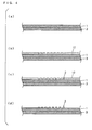
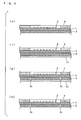
- FIGs. 4 and 5 are sectional views for explaining steps in the method of manufacturing the COF substrate 100 according to the present embodiment.
- the cross section shown in Figs. 4 and 5 corresponds to the cross section taken along the line B-B of Fig. 2 .
- a two-layer base material composed of polyimide and copper is prepared.
- This two-layer base material corresponds to the insulating layer 1 and the metal layer 3 of the COF substrate 100.
- a thinmetal film (not shown) is formed by sputtering on an upper surface of the insulating layer 1.
- a dry film resist 12 having a reverse pattern of the conductive traces 2 ( Fig. 1 ) is formed on the thin metal film as shown in Fig. 4 (b) .
- the reverse pattern is formed by exposure and development of the dry film resist 12.
- the conductive traces 2 are formed by electrolytic plating on exposed portions of the insulating layer 1 (exposed portions of the thin metal film) as shown in Fig. 4 (c) .
- the dry film resist 12 is removed by a stripping liquid while a region, under the dry film resist 12, of the thin metal film is removed by etching as shown in Fig. 4 (d) .
- Electroless tin plating is subsequently performed on surfaces of the conductive traces 2 as surface treatment for connection with the electronic component 5. Then, the cover insulating layer 4 is formed so as to cover a predetermined region of the conductive traces 2 as shown in Fig. 5 (e) .
- a dry film resist 13 is formed on a lower surface of the metal layer excluding regions in which the slits are to be formed, as shown in Fig. 5 (f) . Then, the exposed portions of the metal layer 3 are etched to form the slits 3a as shown in Fig. 5 (g) . After that, the dry film resist 13 is removed by the stripping liquid as shown in Fig. 5 (h) . In this manner, the COF substrate 100 according to the present embodiment is completed.
- the conductive traces 2 may be formed by a subtractive method.
- the pair of slits 3a is formed in the metal layer 3 such that the region being opposite to the electronic component 5 is sandwiched therebetween. This prevents propagation of a stress locally applied to part of the COF substrate 100 to the entire COF substrate 100 through the metal layer 3 at the time of mounting the electronic component 35 or folding the COF substrate 100, for example.
- a stress applied to a region, on an outer side of the pair of slits 3a, of the COF substrate 100 is prevented from being propagated to a region, on an inner side of the pair of slits 3a, of the COF substrate 100.
- a stress applied to the region, on the inner side of the pair of slits 3a, of the COF substrate 100 is prevented from being propagated to the region, on the outer side of the pair of slits 3a, of the COF substrate 100. This prevents disconnection caused by detachment of part of the conductive traces 2 from the insulating layer 1 and separation of the bumps 5a of the electronic component 5 from the terminals 21 of the conductive traces 2.
- the slits 3a are formed such that the metal layer 3 is not divided in the present embodiment. This suppresses propagation of the stress without deterioration of heat dissipation.
- heat dissipation can be sufficiently improved while good connection between the electronic component 5 and the conductive traces 2 is sustained.
- the width W1 and the length L1 of the slits 3a and the distance D3 in the long-side direction between each slit 3a and the opposite region Sa were set to respective various values, and connectivity between the COF substrate 100 and the electronic component 5 and heat dissipation of the COF substrate 100 were examined.
- polyimide was used as a material for the insulating layer 1
- copper was used as a material for the conductive traces 2 and the metal layer 3.
- the thicknesses of the insulating layer 1 and the metal layer 3 were 35 ⁇ m and 15 ⁇ m, respectively.
- the width of each signal line of the conductive traces 2 was 8 ⁇ m, and the distance between the adjacent signal lines in the mounting region S was 12 ⁇ m.
- the length L2 of the shorter sides B1 of the opposite region Sa was 1.6 mm
- the length L4 of the longer sides B2 of the opposite region Sa was 15.1 mm. That is, the electronic component 5 having the shorter sides of 1.6 mm and the longer sides of 15.1 mm, in planar view, was used.
- the length L3 of the metal layer 3 in the short-side direction was 15 mm.
- the length L1 was set to 7 mm
- the distance D3 was set to 3 mm
- the width W1 was set to 0.1 mm, 0.2 mm, 1 mm and 1.5 mm, respectively, in the inventive examples 1 to 4.
- the width W1 was set to 1 mm
- the distance D3 was set to 3 mm
- the length L1 was set to 1 mm, 3 mm, 10 mm and 13 mm, respectively, in the inventive examples 5 to 8.
- the width W1 was set to 1 mm
- the length L1 was set to 7 mm
- the distance D3 was set to 3 mm and 4 mm, respectively, in the inventive examples 9, 10.
- the slits 3a were not formed in the metal layer 3 in the comparative example 1.
- the slits 3a were formed so as to divide the metal layer 3 while the width W1 and the distance D3 were set to 1 mm and 3 mm, respectively.
- a tool temperature was 430 °C
- a stage temperature was 100 °C
- a mounting load was 30 N.
- the tool temperature is a heating temperature of the terminals 21 of the conductive traces 2 or the bumps 5a of the electronic component 5
- the stage temperature is a temperature of a stage on which the COF substrate 100 is placed at the time of mounting the electronic component 5.
- Table 3 shows the disconnection rates of the conductive traces 2 in the inventive examples 1 to 8 and the comparative examples 1, 2.
- the heat of the electronic component 5 was moderately dissipated in the inventive examples 1 to 8, while the heat of the electronic component 5 was not dissipated in the comparative example 2. This shows that the better heat dissipation was secured when the metal layer 3 was not divided by the slits 3a than when the metal layer 3 was divided by the slits 3a.
- the results of the inventive examples 1 to 4 show that the better connection was sustained between the conductive traces 2 and the electronic component 5 when the width W1 of the slits 3a was set in the range from 0.2 to 1.5 mm than when the width W1 of the slits 3a was set to 1 mm.
- results of the inventive examples 5 to 8 show that the better connection was sustained between the conductive traces 2 and the electronic component 5 when the length L1 of the slits 3a was set in the range from 3 to 13 mm than when the length L1 of the slits 3a was set to 1 mm.
- the results of the inventive examples 9, 10 show that the better connection between the conductive traces 2 and the electronic component 5 was sustained when the distance D3 in the long-side direction between each slit 3a and the opposite region Sa was set in the range from 3 to 4 mm.
- Fig. 6 is a diagram showing modifications of the slits 3a formed in the metal layer 3.
- a plurality of slits 6a extend a predetermined length in the short-side direction from one longer side of the metal layer 3, and a plurality of slits 6b extend a predetermined length in the short-side direction from the other longer side of the metal layer 3 in one region and the other region between which the opposite region Sa is sandwiched.
- the slits 6a and the slits 6b are alternately arranged so as not to coincide with one another.
- the propagation of the stress in the metal layer 3 can be sufficiently suppressed by the slits 6a, 6b.
- the metal layer 3 is not divided by the slits 6a, 6b, good heat dissipation can be sustained.
- a plurality of slits 7a extend a predetermined length in the short-side direction from one longer side of the metal layer 3, and a plurality of slits 7b extend a predetermined length in the short-side direction from the other longer side of the metal layer 3 so as to correspond to the plurality of slits 7a, respectively, in one region and the other region between which the opposite region Sa is sandwiched.
- Each slit 7a and the slit 7b corresponding thereto are arranged on the same straight line so as to be spaced from each other.
- Each of slits 7c is formed in a region at the center in the short-side direction and between adjacent two pairs of slits 7a, 7b.
- the propagation of the stress in the metal layer 3 can be sufficiently suppressed by the slits 7a, 7b, 7c. Moreover, since the metal layer 3 is not divided by the slits 7a, 7b, 7c, good heat dissipation can be sustained.
- a plurality of slits 8a and a plurality of slits 8b each having a substantially circular arc shape are formed in one region and the other region, respectively, between which the opposite region Sa is sandwiched.
- the slits 8a and the slits 8b are formed symmetrically to one another with respect to the opposite region Sa.
- the propagation of the stress in the metal layer 3 can be sufficiently suppressed by the slits 8a, 8b.
- the metal layer 3 is not divided by the slits 8a, 8b, good heat dissipation can be sustained.
- the position, number and shape of the slits are not limited to the above-described examples, and may be suitably changed depending on the shape, size or the like of the electronic component 5.
- an opening having another shape such as a round shape or a triangular shape instead of the linear slit may be formed in the metal layer 3.
- the COF substrate 100 is an example of a printed circuit board
- the slits 3a, 6a, 6b, 7a, 7b, 7c, 8a, 8b are examples of an opening
- the slits 3a are examples of first and second slits.
- the material for the insulating layer 1 is not limited to polyimide.
- another insulating material such as polyethylene terephthalate, polyethernitrile, polyethersulfone may be used.
- the material for the conductive traces 2 is not limited to copper.
- another metal material such as copper alloy, gold, aluminum may be used.
- the material for the metal layer 3 is not limited to copper.
- metal having high thermal conductivity such as copper, gold, silver or aluminum is preferably used.
- the present invention is applicable to various printed circuit boards such as a flexible printed circuit board and a rigid printed circuit board.
- the electronic component 5 is not limited to an LSI.
- another electronic component such as a capacitor may be used.
Landscapes
- Engineering & Computer Science (AREA)
- Microelectronics & Electronic Packaging (AREA)
- Structure Of Printed Boards (AREA)
- Wire Bonding (AREA)
- Cooling Or The Like Of Semiconductors Or Solid State Devices (AREA)
- Lead Frames For Integrated Circuits (AREA)
- Electric Connection Of Electric Components To Printed Circuits (AREA)
Applications Claiming Priority (1)
| Application Number | Priority Date | Filing Date | Title |
|---|---|---|---|
| JP2008021273A JP2009182228A (ja) | 2008-01-31 | 2008-01-31 | 配線回路基板およびその製造方法 |
Publications (3)
| Publication Number | Publication Date |
|---|---|
| EP2086295A2 true EP2086295A2 (fr) | 2009-08-05 |
| EP2086295A3 EP2086295A3 (fr) | 2010-05-12 |
| EP2086295B1 EP2086295B1 (fr) | 2011-10-12 |
Family
ID=40637836
Family Applications (1)
| Application Number | Title | Priority Date | Filing Date |
|---|---|---|---|
| EP09250025A Not-in-force EP2086295B1 (fr) | 2008-01-31 | 2009-01-07 | Carte à circuit imprimé et procédé de fabrication correspondant |
Country Status (7)
| Country | Link |
|---|---|
| US (1) | US8581110B2 (fr) |
| EP (1) | EP2086295B1 (fr) |
| JP (1) | JP2009182228A (fr) |
| KR (1) | KR101536360B1 (fr) |
| CN (1) | CN101499454B (fr) |
| AT (1) | ATE528972T1 (fr) |
| TW (1) | TW200942092A (fr) |
Families Citing this family (6)
| Publication number | Priority date | Publication date | Assignee | Title |
|---|---|---|---|---|
| JP5095460B2 (ja) * | 2008-01-17 | 2012-12-12 | シャープ株式会社 | 半導体装置および表示装置 |
| JP5466966B2 (ja) * | 2010-02-16 | 2014-04-09 | 新藤電子工業株式会社 | 配線板、半導体装置、半導体モジュール及びディスプレイ装置 |
| DE102010050343A1 (de) * | 2010-11-05 | 2012-05-10 | Heraeus Materials Technology Gmbh & Co. Kg | Chipintegrierte Durchkontaktierung von Mehrlagensubstraten |
| KR101444883B1 (ko) | 2014-01-27 | 2014-09-26 | 주식회사 기가코리아 | 숫자 url 서비스 제공 방법 |
| KR102616482B1 (ko) | 2018-07-26 | 2023-12-26 | 삼성전자주식회사 | 전원 배선에서 발생된 전자기파를 상쇄하기 위한 접지 배선을 포함하는 인쇄 회로 기판 및 이를 포함하는 전자 장치 |
| CN113518515B (zh) * | 2021-03-15 | 2023-09-08 | 江西宇睿电子科技有限公司 | 断节金属化边制作方法和电路板 |
Citations (2)
| Publication number | Priority date | Publication date | Assignee | Title |
|---|---|---|---|---|
| US20060274252A1 (en) | 2005-06-03 | 2006-12-07 | Samsung Electronics Co., Ltd. | Driver IC package with improved heat dissipation |
| JP2007027682A (ja) | 2005-07-18 | 2007-02-01 | Samsung Electronics Co Ltd | デュアル金属層を有するテープ配線基板及びそれを用いたチップオンフィルムパッケージ |
Family Cites Families (8)
| Publication number | Priority date | Publication date | Assignee | Title |
|---|---|---|---|---|
| JP2844085B2 (ja) * | 1989-07-20 | 1999-01-06 | セイコーインスツルメンツ株式会社 | 回路基板及び半導体素子の実装方法 |
| JP2875076B2 (ja) * | 1990-11-29 | 1999-03-24 | 三井化学株式会社 | フレキシブル配線基板 |
| JP2808952B2 (ja) | 1991-11-27 | 1998-10-08 | 日立電線株式会社 | 半導体素子搭載用基板 |
| FR2796801B1 (fr) * | 1999-07-23 | 2001-10-05 | Valeo Electronique | Assemblage du type comportant une carte a circuit imprime et une semelle formant drain thermique disposes sur une embase formant radiateur |
| JP2001119107A (ja) | 1999-10-19 | 2001-04-27 | Nec Saitama Ltd | プリント配線板 |
| JP3866058B2 (ja) * | 2001-07-05 | 2007-01-10 | シャープ株式会社 | 半導体装置、配線基板及びテープキャリア |
| US7265983B2 (en) * | 2003-10-13 | 2007-09-04 | Tyco Electronics Raychem Gmbh | Power unit comprising a heat sink, and assembly method |
| JP4779826B2 (ja) * | 2006-06-29 | 2011-09-28 | パナソニック株式会社 | フレキシブルプリント基板 |
-
2008
- 2008-01-31 JP JP2008021273A patent/JP2009182228A/ja active Pending
- 2008-12-08 TW TW097147648A patent/TW200942092A/zh unknown
-
2009
- 2009-01-07 EP EP09250025A patent/EP2086295B1/fr not_active Not-in-force
- 2009-01-07 AT AT09250025T patent/ATE528972T1/de not_active IP Right Cessation
- 2009-01-20 US US12/356,106 patent/US8581110B2/en not_active Expired - Fee Related
- 2009-01-24 CN CN2009100019755A patent/CN101499454B/zh not_active Expired - Fee Related
- 2009-01-29 KR KR1020090006953A patent/KR101536360B1/ko not_active Expired - Fee Related
Patent Citations (2)
| Publication number | Priority date | Publication date | Assignee | Title |
|---|---|---|---|---|
| US20060274252A1 (en) | 2005-06-03 | 2006-12-07 | Samsung Electronics Co., Ltd. | Driver IC package with improved heat dissipation |
| JP2007027682A (ja) | 2005-07-18 | 2007-02-01 | Samsung Electronics Co Ltd | デュアル金属層を有するテープ配線基板及びそれを用いたチップオンフィルムパッケージ |
Also Published As
| Publication number | Publication date |
|---|---|
| EP2086295B1 (fr) | 2011-10-12 |
| US20090194321A1 (en) | 2009-08-06 |
| CN101499454B (zh) | 2012-11-07 |
| JP2009182228A (ja) | 2009-08-13 |
| EP2086295A3 (fr) | 2010-05-12 |
| TW200942092A (en) | 2009-10-01 |
| KR101536360B1 (ko) | 2015-07-13 |
| CN101499454A (zh) | 2009-08-05 |
| US8581110B2 (en) | 2013-11-12 |
| ATE528972T1 (de) | 2011-10-15 |
| KR20090084710A (ko) | 2009-08-05 |
Similar Documents
| Publication | Publication Date | Title |
|---|---|---|
| JP5096855B2 (ja) | 配線基板の製造方法及び配線基板 | |
| US10573614B2 (en) | Process for fabricating a circuit substrate | |
| EP2086295B1 (fr) | Carte à circuit imprimé et procédé de fabrication correspondant | |
| EP2086297B1 (fr) | Carte à circuit imprimé et procédé de fabrication correspondant | |
| US8110929B2 (en) | Semiconductor module | |
| JP2022168758A (ja) | フレキシブル配線板、モジュール、及び電子機器 | |
| US8022306B2 (en) | Printed circuit board and method of manufacturing the same | |
| US8102664B2 (en) | Printed circuit board and method of manufacturing the same | |
| US20130029500A1 (en) | Connector and fabrication method thereof | |
| EP1953822A1 (fr) | Carte de circuit imprimé et son procédé de fabrication | |
| JP2013115110A (ja) | 段差構造のプリント配線板 | |
| JP3928152B2 (ja) | プリント配線板 | |
| CN113301712A (zh) | 一种电路板的加工方法及电路板 | |
| JP3867455B2 (ja) | フレキシブル配線基板 | |
| JP2623980B2 (ja) | 半導体搭載用リード付き基板の製造法 | |
| JP5845792B2 (ja) | 電子部品 | |
| CN119603853A (zh) | 电路板和电子设备 | |
| JP2003168852A (ja) | 電子部品の実装方法 | |
| CN114642085A (zh) | 布线电路基板 | |
| JPH0521689A (ja) | 多層リードフレーム | |
| JPH08181244A (ja) | 半導体キャリア |
Legal Events
| Date | Code | Title | Description |
|---|---|---|---|
| PUAI | Public reference made under article 153(3) epc to a published international application that has entered the european phase |
Free format text: ORIGINAL CODE: 0009012 |
|
| AK | Designated contracting states |
Kind code of ref document: A2 Designated state(s): AT BE BG CH CY CZ DE DK EE ES FI FR GB GR HR HU IE IS IT LI LT LU LV MC MK MT NL NO PL PT RO SE SI SK TR |
|
| AX | Request for extension of the european patent |
Extension state: AL BA RS |
|
| PUAL | Search report despatched |
Free format text: ORIGINAL CODE: 0009013 |
|
| AK | Designated contracting states |
Kind code of ref document: A3 Designated state(s): AT BE BG CH CY CZ DE DK EE ES FI FR GB GR HR HU IE IS IT LI LT LU LV MC MK MT NL NO PL PT RO SE SI SK TR |
|
| AX | Request for extension of the european patent |
Extension state: AL BA RS |
|
| 17P | Request for examination filed |
Effective date: 20101105 |
|
| AKX | Designation fees paid |
Designated state(s): AT BE BG CH CY CZ DE DK EE ES FI FR GB GR HR HU IE IS IT LI LT LU LV MC MK MT NL NO PL PT RO SE SI SK TR |
|
| GRAP | Despatch of communication of intention to grant a patent |
Free format text: ORIGINAL CODE: EPIDOSNIGR1 |
|
| GRAC | Information related to communication of intention to grant a patent modified |
Free format text: ORIGINAL CODE: EPIDOSCIGR1 |
|
| RIC1 | Information provided on ipc code assigned before grant |
Ipc: H05K 1/02 20060101AFI20110316BHEP Ipc: H01L 23/34 20060101ALI20110316BHEP |
|
| GRAS | Grant fee paid |
Free format text: ORIGINAL CODE: EPIDOSNIGR3 |
|
| GRAA | (expected) grant |
Free format text: ORIGINAL CODE: 0009210 |
|
| AK | Designated contracting states |
Kind code of ref document: B1 Designated state(s): AT BE BG CH CY CZ DE DK EE ES FI FR GB GR HR HU IE IS IT LI LT LU LV MC MK MT NL NO PL PT RO SE SI SK TR |
|
| REG | Reference to a national code |
Ref country code: GB Ref legal event code: FG4D |
|
| REG | Reference to a national code |
Ref country code: CH Ref legal event code: EP |
|
| REG | Reference to a national code |
Ref country code: IE Ref legal event code: FG4D |
|
| REG | Reference to a national code |
Ref country code: DE Ref legal event code: R096 Ref document number: 602009003035 Country of ref document: DE Effective date: 20111208 |
|
| REG | Reference to a national code |
Ref country code: NL Ref legal event code: VDEP Effective date: 20111012 |
|
| LTIE | Lt: invalidation of european patent or patent extension |
Effective date: 20111012 |
|
| REG | Reference to a national code |
Ref country code: AT Ref legal event code: MK05 Ref document number: 528972 Country of ref document: AT Kind code of ref document: T Effective date: 20111012 |
|
| PG25 | Lapsed in a contracting state [announced via postgrant information from national office to epo] |
Ref country code: BE Free format text: LAPSE BECAUSE OF FAILURE TO SUBMIT A TRANSLATION OF THE DESCRIPTION OR TO PAY THE FEE WITHIN THE PRESCRIBED TIME-LIMIT Effective date: 20111012 Ref country code: IS Free format text: LAPSE BECAUSE OF FAILURE TO SUBMIT A TRANSLATION OF THE DESCRIPTION OR TO PAY THE FEE WITHIN THE PRESCRIBED TIME-LIMIT Effective date: 20120212 Ref country code: NO Free format text: LAPSE BECAUSE OF FAILURE TO SUBMIT A TRANSLATION OF THE DESCRIPTION OR TO PAY THE FEE WITHIN THE PRESCRIBED TIME-LIMIT Effective date: 20120112 Ref country code: LT Free format text: LAPSE BECAUSE OF FAILURE TO SUBMIT A TRANSLATION OF THE DESCRIPTION OR TO PAY THE FEE WITHIN THE PRESCRIBED TIME-LIMIT Effective date: 20111012 |
|
| PG25 | Lapsed in a contracting state [announced via postgrant information from national office to epo] |
Ref country code: PT Free format text: LAPSE BECAUSE OF FAILURE TO SUBMIT A TRANSLATION OF THE DESCRIPTION OR TO PAY THE FEE WITHIN THE PRESCRIBED TIME-LIMIT Effective date: 20120213 Ref country code: SE Free format text: LAPSE BECAUSE OF FAILURE TO SUBMIT A TRANSLATION OF THE DESCRIPTION OR TO PAY THE FEE WITHIN THE PRESCRIBED TIME-LIMIT Effective date: 20111012 Ref country code: GR Free format text: LAPSE BECAUSE OF FAILURE TO SUBMIT A TRANSLATION OF THE DESCRIPTION OR TO PAY THE FEE WITHIN THE PRESCRIBED TIME-LIMIT Effective date: 20120113 Ref country code: LV Free format text: LAPSE BECAUSE OF FAILURE TO SUBMIT A TRANSLATION OF THE DESCRIPTION OR TO PAY THE FEE WITHIN THE PRESCRIBED TIME-LIMIT Effective date: 20111012 Ref country code: HR Free format text: LAPSE BECAUSE OF FAILURE TO SUBMIT A TRANSLATION OF THE DESCRIPTION OR TO PAY THE FEE WITHIN THE PRESCRIBED TIME-LIMIT Effective date: 20111012 Ref country code: SI Free format text: LAPSE BECAUSE OF FAILURE TO SUBMIT A TRANSLATION OF THE DESCRIPTION OR TO PAY THE FEE WITHIN THE PRESCRIBED TIME-LIMIT Effective date: 20111012 Ref country code: NL Free format text: LAPSE BECAUSE OF FAILURE TO SUBMIT A TRANSLATION OF THE DESCRIPTION OR TO PAY THE FEE WITHIN THE PRESCRIBED TIME-LIMIT Effective date: 20111012 |
|
| PG25 | Lapsed in a contracting state [announced via postgrant information from national office to epo] |
Ref country code: CY Free format text: LAPSE BECAUSE OF FAILURE TO SUBMIT A TRANSLATION OF THE DESCRIPTION OR TO PAY THE FEE WITHIN THE PRESCRIBED TIME-LIMIT Effective date: 20111012 |
|
| PG25 | Lapsed in a contracting state [announced via postgrant information from national office to epo] |
Ref country code: DK Free format text: LAPSE BECAUSE OF FAILURE TO SUBMIT A TRANSLATION OF THE DESCRIPTION OR TO PAY THE FEE WITHIN THE PRESCRIBED TIME-LIMIT Effective date: 20111012 Ref country code: SK Free format text: LAPSE BECAUSE OF FAILURE TO SUBMIT A TRANSLATION OF THE DESCRIPTION OR TO PAY THE FEE WITHIN THE PRESCRIBED TIME-LIMIT Effective date: 20111012 Ref country code: CZ Free format text: LAPSE BECAUSE OF FAILURE TO SUBMIT A TRANSLATION OF THE DESCRIPTION OR TO PAY THE FEE WITHIN THE PRESCRIBED TIME-LIMIT Effective date: 20111012 Ref country code: BG Free format text: LAPSE BECAUSE OF FAILURE TO SUBMIT A TRANSLATION OF THE DESCRIPTION OR TO PAY THE FEE WITHIN THE PRESCRIBED TIME-LIMIT Effective date: 20120112 Ref country code: EE Free format text: LAPSE BECAUSE OF FAILURE TO SUBMIT A TRANSLATION OF THE DESCRIPTION OR TO PAY THE FEE WITHIN THE PRESCRIBED TIME-LIMIT Effective date: 20111012 |
|
| PLBE | No opposition filed within time limit |
Free format text: ORIGINAL CODE: 0009261 |
|
| STAA | Information on the status of an ep patent application or granted ep patent |
Free format text: STATUS: NO OPPOSITION FILED WITHIN TIME LIMIT |
|
| PG25 | Lapsed in a contracting state [announced via postgrant information from national office to epo] |
Ref country code: IT Free format text: LAPSE BECAUSE OF FAILURE TO SUBMIT A TRANSLATION OF THE DESCRIPTION OR TO PAY THE FEE WITHIN THE PRESCRIBED TIME-LIMIT Effective date: 20111012 Ref country code: PL Free format text: LAPSE BECAUSE OF FAILURE TO SUBMIT A TRANSLATION OF THE DESCRIPTION OR TO PAY THE FEE WITHIN THE PRESCRIBED TIME-LIMIT Effective date: 20111012 Ref country code: MC Free format text: LAPSE BECAUSE OF NON-PAYMENT OF DUE FEES Effective date: 20120131 Ref country code: RO Free format text: LAPSE BECAUSE OF FAILURE TO SUBMIT A TRANSLATION OF THE DESCRIPTION OR TO PAY THE FEE WITHIN THE PRESCRIBED TIME-LIMIT Effective date: 20111012 |
|
| 26N | No opposition filed |
Effective date: 20120713 |
|
| REG | Reference to a national code |
Ref country code: IE Ref legal event code: MM4A |
|
| REG | Reference to a national code |
Ref country code: DE Ref legal event code: R097 Ref document number: 602009003035 Country of ref document: DE Effective date: 20120713 |
|
| PG25 | Lapsed in a contracting state [announced via postgrant information from national office to epo] |
Ref country code: IE Free format text: LAPSE BECAUSE OF NON-PAYMENT OF DUE FEES Effective date: 20120107 Ref country code: AT Free format text: LAPSE BECAUSE OF FAILURE TO SUBMIT A TRANSLATION OF THE DESCRIPTION OR TO PAY THE FEE WITHIN THE PRESCRIBED TIME-LIMIT Effective date: 20111012 |
|
| PG25 | Lapsed in a contracting state [announced via postgrant information from national office to epo] |
Ref country code: MK Free format text: LAPSE BECAUSE OF FAILURE TO SUBMIT A TRANSLATION OF THE DESCRIPTION OR TO PAY THE FEE WITHIN THE PRESCRIBED TIME-LIMIT Effective date: 20111012 |
|
| PG25 | Lapsed in a contracting state [announced via postgrant information from national office to epo] |
Ref country code: ES Free format text: LAPSE BECAUSE OF FAILURE TO SUBMIT A TRANSLATION OF THE DESCRIPTION OR TO PAY THE FEE WITHIN THE PRESCRIBED TIME-LIMIT Effective date: 20120123 |
|
| PG25 | Lapsed in a contracting state [announced via postgrant information from national office to epo] |
Ref country code: FI Free format text: LAPSE BECAUSE OF FAILURE TO SUBMIT A TRANSLATION OF THE DESCRIPTION OR TO PAY THE FEE WITHIN THE PRESCRIBED TIME-LIMIT Effective date: 20111012 |
|
| PG25 | Lapsed in a contracting state [announced via postgrant information from national office to epo] |
Ref country code: MT Free format text: LAPSE BECAUSE OF FAILURE TO SUBMIT A TRANSLATION OF THE DESCRIPTION OR TO PAY THE FEE WITHIN THE PRESCRIBED TIME-LIMIT Effective date: 20111012 |
|
| REG | Reference to a national code |
Ref country code: CH Ref legal event code: PL |
|
| PG25 | Lapsed in a contracting state [announced via postgrant information from national office to epo] |
Ref country code: CH Free format text: LAPSE BECAUSE OF NON-PAYMENT OF DUE FEES Effective date: 20130131 Ref country code: LI Free format text: LAPSE BECAUSE OF NON-PAYMENT OF DUE FEES Effective date: 20130131 |
|
| PG25 | Lapsed in a contracting state [announced via postgrant information from national office to epo] |
Ref country code: TR Free format text: LAPSE BECAUSE OF FAILURE TO SUBMIT A TRANSLATION OF THE DESCRIPTION OR TO PAY THE FEE WITHIN THE PRESCRIBED TIME-LIMIT Effective date: 20111012 |
|
| PG25 | Lapsed in a contracting state [announced via postgrant information from national office to epo] |
Ref country code: LU Free format text: LAPSE BECAUSE OF NON-PAYMENT OF DUE FEES Effective date: 20120107 |
|
| PG25 | Lapsed in a contracting state [announced via postgrant information from national office to epo] |
Ref country code: HU Free format text: LAPSE BECAUSE OF FAILURE TO SUBMIT A TRANSLATION OF THE DESCRIPTION OR TO PAY THE FEE WITHIN THE PRESCRIBED TIME-LIMIT Effective date: 20090107 |
|
| REG | Reference to a national code |
Ref country code: FR Ref legal event code: PLFP Year of fee payment: 8 |
|
| REG | Reference to a national code |
Ref country code: FR Ref legal event code: PLFP Year of fee payment: 9 |
|
| REG | Reference to a national code |
Ref country code: FR Ref legal event code: PLFP Year of fee payment: 10 |
|
| PGFP | Annual fee paid to national office [announced via postgrant information from national office to epo] |
Ref country code: FR Payment date: 20181213 Year of fee payment: 11 |
|
| PGFP | Annual fee paid to national office [announced via postgrant information from national office to epo] |
Ref country code: GB Payment date: 20190102 Year of fee payment: 11 Ref country code: DE Payment date: 20181228 Year of fee payment: 11 |
|
| REG | Reference to a national code |
Ref country code: DE Ref legal event code: R119 Ref document number: 602009003035 Country of ref document: DE |
|
| GBPC | Gb: european patent ceased through non-payment of renewal fee |
Effective date: 20200107 |
|
| PG25 | Lapsed in a contracting state [announced via postgrant information from national office to epo] |
Ref country code: DE Free format text: LAPSE BECAUSE OF NON-PAYMENT OF DUE FEES Effective date: 20200801 Ref country code: FR Free format text: LAPSE BECAUSE OF NON-PAYMENT OF DUE FEES Effective date: 20200131 Ref country code: GB Free format text: LAPSE BECAUSE OF NON-PAYMENT OF DUE FEES Effective date: 20200107 |