EP2088574A2 - Ansteuerungsschaltung für Anzeigefeld und Anzeigevorrichtung - Google Patents
Ansteuerungsschaltung für Anzeigefeld und Anzeigevorrichtung Download PDFInfo
- Publication number
- EP2088574A2 EP2088574A2 EP09152154A EP09152154A EP2088574A2 EP 2088574 A2 EP2088574 A2 EP 2088574A2 EP 09152154 A EP09152154 A EP 09152154A EP 09152154 A EP09152154 A EP 09152154A EP 2088574 A2 EP2088574 A2 EP 2088574A2
- Authority
- EP
- European Patent Office
- Prior art keywords
- potential
- wirings
- switch
- mosfet
- output
- Prior art date
- Legal status (The legal status is an assumption and is not a legal conclusion. Google has not performed a legal analysis and makes no representation as to the accuracy of the status listed.)
- Withdrawn
Links
- 239000011159 matrix material Substances 0.000 claims description 14
- 238000010586 diagram Methods 0.000 description 11
- 230000007704 transition Effects 0.000 description 9
- 239000004973 liquid crystal related substance Substances 0.000 description 6
- OAICVXFJPJFONN-UHFFFAOYSA-N Phosphorus Chemical compound [P] OAICVXFJPJFONN-UHFFFAOYSA-N 0.000 description 4
- 238000010894 electron beam technology Methods 0.000 description 3
- 238000000034 method Methods 0.000 description 2
- 230000002265 prevention Effects 0.000 description 2
- 230000006641 stabilisation Effects 0.000 description 2
- 238000011105 stabilization Methods 0.000 description 2
- 239000006185 dispersion Substances 0.000 description 1
- 238000012986 modification Methods 0.000 description 1
- 230000004048 modification Effects 0.000 description 1
Images


Classifications
-
- G—PHYSICS
- G09—EDUCATION; CRYPTOGRAPHY; DISPLAY; ADVERTISING; SEALS
- G09G—ARRANGEMENTS OR CIRCUITS FOR CONTROL OF INDICATING DEVICES USING STATIC MEANS TO PRESENT VARIABLE INFORMATION
- G09G3/00—Control arrangements or circuits, of interest only in connection with visual indicators other than cathode-ray tubes
- G09G3/20—Control arrangements or circuits, of interest only in connection with visual indicators other than cathode-ray tubes for presentation of an assembly of a number of characters, e.g. a page, by composing the assembly by combination of individual elements arranged in a matrix no fixed position being assigned to or needed to be assigned to the individual characters or partial characters
- G09G3/22—Control arrangements or circuits, of interest only in connection with visual indicators other than cathode-ray tubes for presentation of an assembly of a number of characters, e.g. a page, by composing the assembly by combination of individual elements arranged in a matrix no fixed position being assigned to or needed to be assigned to the individual characters or partial characters using controlled light sources
-
- G—PHYSICS
- G09—EDUCATION; CRYPTOGRAPHY; DISPLAY; ADVERTISING; SEALS
- G09G—ARRANGEMENTS OR CIRCUITS FOR CONTROL OF INDICATING DEVICES USING STATIC MEANS TO PRESENT VARIABLE INFORMATION
- G09G2300/00—Aspects of the constitution of display devices
- G09G2300/04—Structural and physical details of display devices
- G09G2300/0439—Pixel structures
- G09G2300/0465—Improved aperture ratio, e.g. by size reduction of the pixel circuit, e.g. for improving the pixel density or the maximum displayable luminance or brightness
-
- G—PHYSICS
- G09—EDUCATION; CRYPTOGRAPHY; DISPLAY; ADVERTISING; SEALS
- G09G—ARRANGEMENTS OR CIRCUITS FOR CONTROL OF INDICATING DEVICES USING STATIC MEANS TO PRESENT VARIABLE INFORMATION
- G09G2310/00—Command of the display device
- G09G2310/02—Addressing, scanning or driving the display screen or processing steps related thereto
- G09G2310/0264—Details of driving circuits
- G09G2310/0289—Details of voltage level shifters arranged for use in a driving circuit
-
- G—PHYSICS
- G09—EDUCATION; CRYPTOGRAPHY; DISPLAY; ADVERTISING; SEALS
- G09G—ARRANGEMENTS OR CIRCUITS FOR CONTROL OF INDICATING DEVICES USING STATIC MEANS TO PRESENT VARIABLE INFORMATION
- G09G2310/00—Command of the display device
- G09G2310/02—Addressing, scanning or driving the display screen or processing steps related thereto
- G09G2310/0264—Details of driving circuits
- G09G2310/0297—Special arrangements with multiplexing or demultiplexing of display data in the drivers for data electrodes, in a pre-processing circuitry delivering display data to said drivers or in the matrix panel, e.g. multiplexing plural data signals to one D/A converter or demultiplexing the D/A converter output to multiple columns
-
- G—PHYSICS
- G09—EDUCATION; CRYPTOGRAPHY; DISPLAY; ADVERTISING; SEALS
- G09G—ARRANGEMENTS OR CIRCUITS FOR CONTROL OF INDICATING DEVICES USING STATIC MEANS TO PRESENT VARIABLE INFORMATION
- G09G2320/00—Control of display operating conditions
- G09G2320/02—Improving the quality of display appearance
- G09G2320/0223—Compensation for problems related to R-C delay and attenuation in electrodes of matrix panels, e.g. in gate electrodes or on-substrate video signal electrodes
-
- G—PHYSICS
- G09—EDUCATION; CRYPTOGRAPHY; DISPLAY; ADVERTISING; SEALS
- G09G—ARRANGEMENTS OR CIRCUITS FOR CONTROL OF INDICATING DEVICES USING STATIC MEANS TO PRESENT VARIABLE INFORMATION
- G09G2320/00—Control of display operating conditions
- G09G2320/02—Improving the quality of display appearance
- G09G2320/0233—Improving the luminance or brightness uniformity across the screen
-
- G—PHYSICS
- G09—EDUCATION; CRYPTOGRAPHY; DISPLAY; ADVERTISING; SEALS
- G09G—ARRANGEMENTS OR CIRCUITS FOR CONTROL OF INDICATING DEVICES USING STATIC MEANS TO PRESENT VARIABLE INFORMATION
- G09G2330/00—Aspects of power supply; Aspects of display protection and defect management
- G09G2330/02—Details of power systems and of start or stop of display operation
- G09G2330/025—Reduction of instantaneous peaks of current
-
- G—PHYSICS
- G09—EDUCATION; CRYPTOGRAPHY; DISPLAY; ADVERTISING; SEALS
- G09G—ARRANGEMENTS OR CIRCUITS FOR CONTROL OF INDICATING DEVICES USING STATIC MEANS TO PRESENT VARIABLE INFORMATION
- G09G2330/00—Aspects of power supply; Aspects of display protection and defect management
- G09G2330/02—Details of power systems and of start or stop of display operation
- G09G2330/028—Generation of voltages supplied to electrode drivers in a matrix display other than LCD
-
- G—PHYSICS
- G09—EDUCATION; CRYPTOGRAPHY; DISPLAY; ADVERTISING; SEALS
- G09G—ARRANGEMENTS OR CIRCUITS FOR CONTROL OF INDICATING DEVICES USING STATIC MEANS TO PRESENT VARIABLE INFORMATION
- G09G3/00—Control arrangements or circuits, of interest only in connection with visual indicators other than cathode-ray tubes
- G09G3/20—Control arrangements or circuits, of interest only in connection with visual indicators other than cathode-ray tubes for presentation of an assembly of a number of characters, e.g. a page, by composing the assembly by combination of individual elements arranged in a matrix no fixed position being assigned to or needed to be assigned to the individual characters or partial characters
- G09G3/2007—Display of intermediate tones
- G09G3/2014—Display of intermediate tones by modulation of the duration of a single pulse during which the logic level remains constant
-
- H—ELECTRICITY
- H03—ELECTRONIC CIRCUITRY
- H03K—PULSE TECHNIQUE
- H03K17/00—Electronic switching or gating, i.e. not by contact-making and –breaking
- H03K17/16—Modifications for eliminating interference voltages or currents
- H03K17/161—Modifications for eliminating interference voltages or currents in field-effect transistor switches
- H03K17/165—Modifications for eliminating interference voltages or currents in field-effect transistor switches by feedback from the output circuit to the control circuit
- H03K17/166—Soft switching
- H03K17/167—Soft switching using parallel switching arrangements
Definitions
- the present invention relates to a drive circuit of a display panel and a display apparatus.
- Such a kind of display apparatuses has a display panel (matrix panel) where a lot of display devices are arranged in a matrix pattern, and a drive circuit which drives the display devices.
- Japanese Patent Application Laid-Open No. 2003-131611 discloses a drive circuit of a display apparatus which controls feedback of a voltage using an operational amplifier.
- a phase characteristic of an amplifier should be secured over a wide output voltage range including selection potential through non-selection potential.
- Japanese Patent Application Laid-Open No. 2004-4429 discloses a drive circuit which uses a combination of a plurality of MOSFETs having different ON-state resistances. In this circuit configuration, however, in order to avoid voltage drop caused by the ON-state resistances of the MOSFETs, the size of the MOSFETs should be increased.
- FIGS. 2A and 2B are diagrams illustrating a constitution of the image display apparatus, FIG. 2A is a plan view, and FIG. 2B is a cross-sectional view.
- the image display apparatus includes a matrix panel (display panel) 1, a control unit 4, a scan driving unit 5 and a modulation driving unit 6.
- the scan driving unit 5 and the modulation driving unit 6 are composed of ICs (integrated circuits) respectively.
- the matrix panel 1 has a rear plate 1A on which a plurality of electron-emitting devices 3A (also as electron sources) is arranged, and a face plate 3B on which a phosphor 3C is arranged. Surface conduction electron-emitting devices are used as the electron-emitting devices 3A.
- the electron-emitting devices on the rear plate 1A are matrix-driven through scanning wirings 2 and modulation wirings 3 .
- the scanning wirings 2 are connected to output terminals of the scan driving unit 5 via a flexible printed wiring board (FPC) or the like.
- the modulation wirings 3 are connected to output terminals of the modulation driving unit 6 via FPC or the like.
- the control unit 4 controls the scan driving unit 5 and the modulation driving unit 6, and a driving voltage of several dozen bolts is applied between the scanning wirings 2 and the modulation wirings 3.
- a driving voltage of several dozen bolts is applied between the scanning wirings 2 and the modulation wirings 3.
- electrons are emitted from the electron-emitting devices 3A.
- a high voltage of several kV to several dozen kV is applied to the face plate 3B.
- the electrons emitted from the electron-emitting devices 3A are attracted to the face plate 3B, and collide against the phosphor 3C.
- Brightness at this time is determined by an amount of the electrons colliding against the phosphor 3C in a predetermined period. Therefore, the brightness can be controlled by a value of the driving voltage or an applying period or both of them. As a result, gradation display is enabled.
- the control unit 4 controls voltages of a scanning signal to be applied to the scanning wirings 2 and a modulation signal to be applied to the modulation wirings 3, so that various videos are displayed.
- the brightness obtained by light emission from the phosphor 3C is determined by the driving voltage of the electron-emitting devices (a potential difference between the scanning signal and the modulation signal) . Therefore, in order to obtain accurate luminance characteristics, stabilization of the driving voltage of the electron-emitting devices 3A, namely, prevention of waveform disturbance of the driving voltage (overshoot, undershoot, ringing, and the like) becomes important.
- the scan driving unit 5 is a drive circuit which selects one or a plurality of scanning wirings 2.
- the scan driving unit 5 applies a selection potential to the scanning wirings 2 to be selected, and applies a non-selection potential to the other scanning wirings 2.
- the scanning wirings 2 to be selected are sequentially switched, so that scanning in a vertical direction is realized.
- the scan driving unit 5 is composed of integrated circuits. If one integrated circuit scans all the scanning wirings, a difference in path lengths from the integrated circuit to the respective scanning wirings becomes large. In order to solve this problem, a plurality (four) of integrated circuits are used so as to compose the scan driving unit 5 in this embodiment.
- the modulation driving unit 6 is a drive circuit which applies a modulation signal modulated based on an input image signal to the modulation wirings 3 .
- the modulation signal is generated from an output of single or a plurality of constant voltage power sources.
- the modulation driving unit 6 is also composed of several integrated circuits (five integrated circuits in this embodiment) .
- the modulation signal having a pulse width modulation waveform of plus several dozen V is used.
- the wider the pulse width is, the larger the integrated value of luminance becomes, and the brighter the device becomes.
- the luminance of the display device on line N+1 is higher than that of the display device on line N.
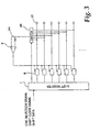
- FIG. 3 is a block diagram of the scan driving unit 5. As shown in FIG. 3 , the scan driving unit 5 has a shift register unit 7, buffered switches 8, a feedback switch 9B and a feedback amplifier 9.
- the shift register unit 7 is a logic circuit which determines a line to be selected, and generates/outputs a control signal.
- the shift register unit 7 includes a shift register composed of D flip-flops, not shown, and a logic device which performs logical operations on an output from the shift register, a shift clock and an output of shift data.
- the buffered switches 8 are circuits which convert shift data (control signal) output from the shift register unit 7 into a voltage/current level necessary for driving the scanning wirings and output the converted data.
- the feedback switch 9B is a circuit that selects which IC driving output (output pad) 10 to be connected to the input 9A of the amplifier 9 based on the signal from the shift register unit 7.
- a potential of a selected line (scanning wiring) is fed back to the amplifier 9.
- a selection potential V1 is connected as a reference potential REF to the other input of the amplifier 9.
- the amplifier 9 compares the potential of the selected scanning wiring with the reference potential REF so as to control the buffered switch 8 using a signal according to the difference therebetween. As a result, the potential of the selected scanning wiring is maintained at the reference potential REF.
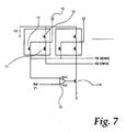
- An N-ch MOSFET for feedback 13 in FIG. 7 corresponds to the feedback switch 9B in FIG. 3 .
- a strong drive performance P-ch MOSFET (P-ch MOSFET of a high drive performance) 12 controls the IC driving output 10 to the non-selection potential V2 so as to regulate the potential of the scanning wiring to the non-selection potential V2.
- a strong drive performance N-ch MOSFET (N-ch MOSFET of a high drive performance) 11 regulates the potential of the scanning wiring to the selection potential V1 .
- a source terminal of the strong drive performance N-ch MOSFET 11 for each scanning wiring is connected to a common line, and the common line is connected to an output terminal of an OPAMP (operational amplifier) 15 via an AMP_N-ch MOSFET 14.
- An N-line FB selection SW signal 101 shown in FIG. 8 is input into the N-ch MOSFET 13 for feedback during a selection period.
- the N-ch MOSFET 13 for feedback is then turned on, and the potential of the selected IC driving output 10 is fed back to the OPAMP 15.
- the potential of the IC driving output 10 is lower than the selection potential V1 due to voltage drop caused by an electric current flowing in the scanning wirings and ON-state resistance of the strong drive performance N-ch MOSFET 11.
- the OPAMP 15 compares the potential of the IC driving output 10 with the reference potential (selection potential V1), and controls the AMP_N-ch MOSFET 14 so that the IC driving output 10 becomes the reference potential. As a result, an N-line output waveform 103 as shown in FIG. 8 can be obtained.
- FIG. 1 illustrates only a constitution of output circuits for two channels, but the output circuits are provided so as to correspond to the number of channels (the number of scanning wirings) .
- a feedback amplifier is commonly-provided for the plurality of channels.
- the IC driving output 10 is an output pad which is connected to the scanning wiring 2.
- the two switches including the strong drive performance P-ch MOSFET 12 and the weak drive performance P-ch MOSFET (P-ch MOSFET of a low drive performance) 17 are connected as driving means for the non-selection potential V2 to the scanning wirings in parallel.
- the strong drive performance P-ch MOSFET 12 drives the scanning wiring 2 to the non-selection potential V2.
- the weak drive performance P-ch MOSFET 17 is a switch whose drive performance is lower than the that of the strong drive performance P-ch MOSFET 12 (for example, ON-state resistance is ten times higher), and is used for transition of the potential of the scanning wiring from the selection potential to the non-selection potential.
- the N-ch MOSFET 13 for feedback is a switch which connects the potential of the selected scanning wiring (driven by the selection potential) to an input of the OPAMP 15.
- a feedback off switch 18 is a switch which fixes the output of the OPAMP 15 at the reference potential when the potential of the scanning wiring is transited from the selection potential to the non-selection potential or from the non-selection potential to the selection potential.
- a signal whose waveform is same as that of a shift clock 200 (see FIG. 4 ) and whose level is shifted is input into the gate of the feedback off switch 18.
- Lo is a drain voltage of the AMP_N-ch MOSFET 14
- Hi is its drain voltage ( 5 V.
- the feedback off switch 18 is turned on for during a potential transition period of the scanning wiring, namely, no scanning wiring is at the selection potential .
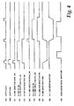
- a driving method of the scanning wirings is concretely described below with reference to FIG. 4 .
- the ON-state resistance of the weak drive performance N-ch MOSFET 16 is set to several dozen ⁇ to several dozens k ⁇ so that waveform disturbance (overshoot, undershoot, ringing and the like) does not occur at the time of the potential transition.
- the potential of the scanning wiring is controlled to the selection potential.
- the shift register unit 7 outputs an N-line FB_SW/N-line selection AMP_SW signal 202.
- This signal is shifted by a level shifter in the buffered switch 8 to a voltage level at which the gate of the strong drive performance N-ch MOSFET 11 and the gate of the N-ch MOSFET 13 for feedback can be driven.
- the strong drive performance N-ch MOSFET 11 and the N-ch MOSFET 13 for feedback are simultaneously turned on.
- the N-line FB_SW/N-line selection AMP_SW signal 202 is inverted, and its level is shifted in order to turn off the feedback off switch 18.
- the potential of the selected scanning wiring is controlled to the reference potential (selection potential (for example, -10 V)).
- Such feedback control corrects an influence of the voltage drop due to a current change of the scanning wirings 2 and the ON-state resistance of the strong drive performance N-ch MOSFET 11, so that the potentials of the scanning wirings can be maintained constant.
- the N-line FB_SW/N-line selection AMP_SW signal 202 is Lo
- the N-line IC driving output 10 is disconnected from the feedback circuit.
- an N+1-line selection WEAK_SW signal 204 is level-shifted.
- the weak drive performance N-ch MOSFET 16 for line N+1 is turned on and the weak drive performance P-ch MOSFET 17 for line N is turned on during a period where the N+1-line selection WEAK_SW signal 204 is Hi.
- the ON-state resistance of the weak drive performance P-ch MOSFET 17 is set to several dozen ⁇ to several dozen k ⁇ so that waveform disturbance does not occur at the time of the potential transition.
- an N-line driving waveform 207 stably transits from the selection potential to the non-selection potential. Thereafter, the strong drive performance P-ch MOSFET 12 fixes the N-Line IC driving output to the non-selection potential.
- the potential (selection potential) of the driving signal on the scanning wiring is maintained at an appropriate value by the feedback control of the OPAMP 15. Since the switch of a low drive performance is used at the time of potential transition, an abrupt change in potential can be suppressed, so that the waveform disturbance such as overshoot, undershoot or ringing can be prevented. Since timing at which the OPAMP 15 operates is after the transition to the selection potential by means of the weak drive performance N-ch MOSFET 16, the output potential of the OPAMP 15 hardly deviates from around -10 V which is the reference potential (selection potential). For this reason, requirements of the slew rate and the AMP band may be ensured within a small voltage range of around -10 V. The switches exclusively used for the voltage transition are provided, so that performance demand for the OPAMP 15 is relaxed. Therefore, the highly reliable drive circuit with a feedback amplifier can be manufactured inexpensively.
- the switching from the switch driving into the AMP driving is controlled by the control signal transmitted from the shift register unit 7.
- a logic circuit such as the shift register is operated by a low voltage (for example, 3.3 V) .
- the voltage level of the control signal should be shifted by the level shifter.
- the switching from the switch driving into the AMP driving is realized by a self switch (control circuit) in the buffered switch 8.
- the circuit configuration is simplified and the accurate switching timing from a switch into AMP is realized. Since the other parts of the constitution are similar to those of the first embodiment, the characteristic constitution of the second embodiment is mainly described below.
- FIG. 5 is a block diagram illustrating the scan driving unit according to the second embodiment.
- a self switch 19 for P-ch is connected to the gate of the strong drive performance P-ch MOSFET 12.
- the self switch 19 for P-ch is a circuit which outputs a control signal for controlling the strong drive performance P-ch MOSFET 12 according to an output from the weak drive performance P-ch MOSFET 17.
- An self switch 20 for N-ch is connected to the gate of the strong drive performance N-ch MOSFET 11.
- the self switch 20 for N-ch is a circuit which outputs a control signal for controlling the strong drive performance N-ch MOSFET 11 (second switch) according to an output from the weak drive performance N-ch MOSFET 16 (first switch).
- FIG. 6 illustrates a circuit configuration of the self switch.
- the self switch includes a voltage comparator 43 composed of an operational amplifier, and an AND gate circuit 44.
- the self switch 19 for P-ch and the self switch 20 for N-ch have the same basic constitution.
- One input 40 of the voltage comparator 43 is connected to the scanning wirings (the outputs of the weak performance MOSFETs 16 and 17), and the other input 41 of the voltage comparator 43 is connected to a standard potential.
- the reference potential is set to a potential lower than the non-selection potential V2 (for example, V2-1 volts).
- the self switch 20 for N-ch the reference potential is set to a potential higher than the selection potential V1 (for example, V1+1 volts).
- VC and VE are power source terminals of the voltage comparator 43. Since the voltage comparator 43 treats an input/output voltage equivalent to the selection potential V1 or the non-selection potential V2, a power supply voltage according to the input/output voltage is necessary.
- VC is connected to GND
- VE is connected to a power source of the selection potential V1 minus several V (for example, V1-5 volts) .
- a power supply voltage (for example, 5 volts or more volts to several dozens volts) higher than the power supply voltage (for example, not more than 3.3 volts) to be supplied to the shift register unit 7 is supplied to the self switches.
- One input of the AND gate circuit 44 is connected to an output of the voltage comparator 43 and the other input of the AND gate circuit 44 is connected to a gate of the WEAK_MOSFET (output of the level shifter).
- An output of the AND gate circuit 44 is connected to a gate of a STRONG_MOSFET.
- the weak drive performance P-ch MOSFET 17 is turned on, and the potential of the output 10 rises toward the non-selection potential V2.
- the voltage comparator 43 of the self switch 19 for P-ch compares the potential of the output 10 with the reference potential (for example, V2-1 volts) . When the potential of the output 10 exceeds the reference potential, the voltage comparator 43 outputs an ON signal.
- the AND gate circuit 44 obtains AND of the output from the voltage comparator 43 and a signal obtained by inverting a gate control signal of the weak drive performance P-ch MOSFET 17.
- the weak drive performance N-ch MOSFET 16 is turned on and the potential of the output 10 drops toward the selection potential V1.
- the voltage comparator 43 of the self switch 20 for N-ch compares the potential of the output 10 with the reference potential (for example, V1+1 volts) . When the potential of the output 10 is lower than the reference potential, the voltage comparator 43 outputs an ON signal.
- the AND gate circuit 44 obtains AND of the output from the voltage comparator 43 and a voltage of a gate control signal from the weak drive performance N-ch MOSFET 16.
- the gate control signal is output from the AND gate circuit 44 to the strong drive performance N-ch MOSFET 11 .
- the strong drive performance N-ch MOSFET 11 is turned on.
- the ON state of the strong drive performance N-ch MOSFET 11 is maintained by the latch circuit, not shown, until the weak drive performance P-ch MOSFET 17 is turned on.
- the driving of the MOSFETs is controlled at the timing of the level shifters, the high-speed and accurate level shifters are necessary.
- the self switch automatically starts the driving of the strong performance MOSFET according to the output potential (namely, when the output potential reaches the target value). Therefore, the respective MOSFETs can be driven at appropriate and accurate timings. Since requirements of the accuracy are reduced, the circuit can be simplified. Further, since the number of the level shifters can be greatly reduced, a chip area of the driving IC can be reduced.
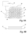
- FIGS. 9A and 9B are diagrams illustrating a constitution for driving the LED backlight of the liquid crystal display apparatus, FIG. 9A is a plan view, and FIG. 9B is a cross-sectional view.
- the LED backlight of the liquid crystal display apparatus has an LED matrix 51, a control unit 56, a line driving unit 57 and a column driving unit 58.
- the line driving unit 57 and the column driving unit 58 are respectively composed of an IC (integrated circuit).
- the LED matrix 51 in which a plurality of LED blocks 54 (LEDs are connected in series) is arranged, emits light toward a liquid crystal panel 55 from the back of it so that a desired image is displayed.
- the LED blocks 54 on the LED matrix 51 are matrix-driven by line selection wirings 52 and column selection wirings 53.
- the line selection wirings 52 are respectively connected to output terminals of the line driving unit 57 via resistances 59.
- the column selection wirings 53 are respectively connected to output terminals of the column driving unit 58.
- the control unit 56 controls the line driving unit 57 and the column driving unit 58, and applies a driving voltage of several dozen volts, for example, between the line selection wirings 52 and the column selection wirings 53 via the resistances 59.
- the LED blocks 54 emit light.
- the LED blocks emit light according to a video on the liquid crystal panel 55, so that bright portions of the screen emit light brightly, and dark portions of the screen emit light slightly. As a result, luminance control (local dimming) according to the video is enabled.
- control unit 56 controls the timing of the switching the column selection wirings 53, the selection time, and the timing at which a voltage is applied to the line selection wirings 52. As a result, the luminance control is made in synchronization with the video.
- the brightness obtained by the light emission of the LED blocks 54 is determined by applied voltages to the LED blocks 54 (applied currents to the LED blocks 54 controlled by the resistances 59) . Therefore, in order to obtain the accurate luminance characteristics without dispersion, the stabilization of the driving voltage (driving current) of the LED blocks 54, namely, prevention of the waveform disturbance of the driving voltage (overshoot, undershoot, ringing and the like) becomes important.
- the line driving unit 57 is a drive circuit which selects one or a plurality of line selecting wirings 52.
- the line driving unit 57 applies a selection potential of minus several dozen V to the line selection wirings 52 to be selected, and applies a GND potential to the other line selection wirings 52.
- the line selection wirings 52 to be selected are sequentially switched, so that the selection of the LED blocks 54 in a vertical direction is realized.
- the line driving unit 57 is composed of an integrated circuit.
- the column driving unit 58 is a drive circuit which selects the column selection wirings 53 based on an input image signal, controls selection time and controls an amount of light emission from the respective LED blocks 54.
- the line driving unit 57 and the column driving unit 58 are realized by using the circuit configurations of the scan driving unit 5 and the modulation driving unit 6 in the first and second embodiments.
- overshoot, undershoot and ringing can be repressed.
- the voltage (electric current) and the time for applying to the LED blocks 54 can be accurately controlled, the accurate luminance control is achieved, and the high-definition video display is achieved.
- a drive circuit for driving a display panel having wirings and display devices to be connected to the wirings has a first switch that transits potential of the wirings toward the first potential, a feedback amplifier that maintains the potentials of the wirings at the first potential, and a second switch that selects whether or not to supply an output from the feedback amplifier to the wirings.
- the first switch and the second switch are connected to the wirings in parallel.
- a drive performance of the first switch is lower than that of the feedback amplifier.
Landscapes
- Engineering & Computer Science (AREA)
- Physics & Mathematics (AREA)
- Computer Hardware Design (AREA)
- General Physics & Mathematics (AREA)
- Theoretical Computer Science (AREA)
- Control Of Indicators Other Than Cathode Ray Tubes (AREA)
- Liquid Crystal (AREA)
- Liquid Crystal Display Device Control (AREA)
- Electroluminescent Light Sources (AREA)
Applications Claiming Priority (2)
| Application Number | Priority Date | Filing Date | Title |
|---|---|---|---|
| JP2008026346 | 2008-02-06 | ||
| JP2009000850A JP2009211053A (ja) | 2008-02-06 | 2009-01-06 | 表示パネルの駆動回路および表示装置 |
Publications (2)
| Publication Number | Publication Date |
|---|---|
| EP2088574A2 true EP2088574A2 (de) | 2009-08-12 |
| EP2088574A3 EP2088574A3 (de) | 2010-04-14 |
Family
ID=40568446
Family Applications (1)
| Application Number | Title | Priority Date | Filing Date |
|---|---|---|---|
| EP09152154A Withdrawn EP2088574A3 (de) | 2008-02-06 | 2009-02-05 | Ansteuerungsschaltung für Anzeigefeld und Anzeigevorrichtung |
Country Status (3)
| Country | Link |
|---|---|
| US (1) | US8154540B2 (de) |
| EP (1) | EP2088574A3 (de) |
| JP (1) | JP2009211053A (de) |
Families Citing this family (2)
| Publication number | Priority date | Publication date | Assignee | Title |
|---|---|---|---|---|
| JP2009211052A (ja) * | 2008-02-06 | 2009-09-17 | Canon Inc | 表示パネルの駆動回路および表示装置 |
| KR101887837B1 (ko) | 2009-12-18 | 2018-08-10 | 가부시키가이샤 한도오따이 에네루기 켄큐쇼 | 광 센서를 포함하는 표시 장치 및 그 구동 방법 |
Citations (2)
| Publication number | Priority date | Publication date | Assignee | Title |
|---|---|---|---|---|
| JP2003131611A (ja) | 2001-07-31 | 2003-05-09 | Canon Inc | 走査回路及び画像表示装置 |
| JP2004004429A (ja) | 2001-08-03 | 2004-01-08 | Canon Inc | 画像表示装置 |
Family Cites Families (12)
| Publication number | Priority date | Publication date | Assignee | Title |
|---|---|---|---|---|
| US5880624A (en) * | 1994-07-08 | 1999-03-09 | Kabushiki Kaisha Toshiba | Constant potential generating circuit and semiconductor device using same |
| US5877647A (en) * | 1995-10-16 | 1999-03-02 | Texas Instruments Incorporated | CMOS output buffer with slew rate control |
| JP3930992B2 (ja) * | 1999-02-10 | 2007-06-13 | 株式会社日立製作所 | 液晶表示パネル用駆動回路及び液晶表示装置 |
| US6970162B2 (en) | 2001-08-03 | 2005-11-29 | Canon Kabushiki Kaisha | Image display apparatus |
| JP3715967B2 (ja) | 2002-06-26 | 2005-11-16 | キヤノン株式会社 | 駆動装置及び駆動回路及び画像表示装置 |
| JP4332358B2 (ja) * | 2003-01-30 | 2009-09-16 | キヤノン株式会社 | 駆動回路 |
| US7812794B2 (en) | 2004-12-06 | 2010-10-12 | Semiconductor Energy Laboratory Co., Ltd. | Display device and driving method thereof |
| JP2006330701A (ja) * | 2005-04-26 | 2006-12-07 | Canon Inc | 走査回路、走査装置、画像表示装置およびテレビジョン装置 |
| JP2006318381A (ja) * | 2005-05-16 | 2006-11-24 | Seiko Epson Corp | 電圧発生回路 |
| DE602005016539D1 (de) | 2005-07-07 | 2009-10-22 | St Microelectronics Srl | Selbstanpassender Ausgangspuffer basierend auf Ladungsverteilung |
| JP2008256915A (ja) | 2007-04-04 | 2008-10-23 | Canon Inc | 表示パネルの駆動回路及び画像表示装置 |
| JP2009211052A (ja) * | 2008-02-06 | 2009-09-17 | Canon Inc | 表示パネルの駆動回路および表示装置 |
-
2009
- 2009-01-06 JP JP2009000850A patent/JP2009211053A/ja not_active Withdrawn
- 2009-01-30 US US12/362,882 patent/US8154540B2/en not_active Expired - Fee Related
- 2009-02-05 EP EP09152154A patent/EP2088574A3/de not_active Withdrawn
Patent Citations (2)
| Publication number | Priority date | Publication date | Assignee | Title |
|---|---|---|---|---|
| JP2003131611A (ja) | 2001-07-31 | 2003-05-09 | Canon Inc | 走査回路及び画像表示装置 |
| JP2004004429A (ja) | 2001-08-03 | 2004-01-08 | Canon Inc | 画像表示装置 |
Also Published As
| Publication number | Publication date |
|---|---|
| US8154540B2 (en) | 2012-04-10 |
| EP2088574A3 (de) | 2010-04-14 |
| JP2009211053A (ja) | 2009-09-17 |
| US20090195522A1 (en) | 2009-08-06 |
Similar Documents
| Publication | Publication Date | Title |
|---|---|---|
| EP2096621A2 (de) | Ansteuerungsschaltung für Anzeigetafel und Anzeigevorrichtung | |
| US10726774B2 (en) | Backlight driving circuit and method, backlight module, backlight circuit and display device | |
| US10694597B2 (en) | LED pixel circuits with PWM dimming | |
| CN110718195B (zh) | 发光装置、显示装置及led显示装置 | |
| KR100512833B1 (ko) | 자기 발광형 표시 장치 | |
| US20200051484A1 (en) | Backlight device and display device provided with same | |
| CN111613185B (zh) | 发光元件驱动装置、发光元件驱动系统及发光系统 | |
| KR100675244B1 (ko) | 표시 장치 및 그 제어 방법 | |
| US10935843B2 (en) | Backlight and display device provided with same | |
| EP4207158A1 (de) | Anzeigegerät | |
| CN115985212B (zh) | 电子装置 | |
| KR20090118225A (ko) | 표시 장치 및 그 구동 방법 | |
| CN118355426A (zh) | 显示面板的驱动电路 | |
| US20220335905A1 (en) | Light-emitting device, display device, and led display device | |
| JP7101463B2 (ja) | 発光素子駆動装置、半導体装置、発光装置及び液晶表示装置 | |
| US8154540B2 (en) | Drive circuit of display panel and display apparatus | |
| EP2088573A2 (de) | Ansteuerungsschaltung für Anzeigefeld und Anzeigevorrichtung | |
| JP2003108075A (ja) | 表示装置およびその駆動方法 | |
| KR20030004774A (ko) | 전류 구동형 표시소자의 구동 회로 | |
| US12260804B2 (en) | Pixel circuit and display panel | |
| US7535439B2 (en) | Display device and method for driving a display device | |
| US11727865B1 (en) | Light-emitting diode driver and display apparatus using the same | |
| US8248354B2 (en) | Driving circuit and image display apparatus | |
| KR20090067140A (ko) | 백라이트 디바이스를 위한 발광 다이오드 소자 세트 및 백라이트 디스플레이 | |
| US20240397595A1 (en) | Load drive circuit, light emitting diode driver, and display device |
Legal Events
| Date | Code | Title | Description |
|---|---|---|---|
| PUAI | Public reference made under article 153(3) epc to a published international application that has entered the european phase |
Free format text: ORIGINAL CODE: 0009012 |
|
| AK | Designated contracting states |
Kind code of ref document: A2 Designated state(s): AT BE BG CH CY CZ DE DK EE ES FI FR GB GR HR HU IE IS IT LI LT LU LV MC MK MT NL NO PL PT RO SE SI SK TR |
|
| AX | Request for extension of the european patent |
Extension state: AL BA RS |
|
| PUAL | Search report despatched |
Free format text: ORIGINAL CODE: 0009013 |
|
| AK | Designated contracting states |
Kind code of ref document: A3 Designated state(s): AT BE BG CH CY CZ DE DK EE ES FI FR GB GR HR HU IE IS IT LI LT LU LV MC MK MT NL NO PL PT RO SE SI SK TR |
|
| AX | Request for extension of the european patent |
Extension state: AL BA RS |
|
| 17P | Request for examination filed |
Effective date: 20101014 |
|
| AKX | Designation fees paid |
Designated state(s): DE FR GB |
|
| 17Q | First examination report despatched |
Effective date: 20110110 |
|
| STAA | Information on the status of an ep patent application or granted ep patent |
Free format text: STATUS: THE APPLICATION HAS BEEN WITHDRAWN |
|
| 18W | Application withdrawn |
Effective date: 20110203 |