EP2090928A2 - Appareil d'impression, procédé d'impression et moule pour impression - Google Patents
Appareil d'impression, procédé d'impression et moule pour impression Download PDFInfo
- Publication number
- EP2090928A2 EP2090928A2 EP09159207A EP09159207A EP2090928A2 EP 2090928 A2 EP2090928 A2 EP 2090928A2 EP 09159207 A EP09159207 A EP 09159207A EP 09159207 A EP09159207 A EP 09159207A EP 2090928 A2 EP2090928 A2 EP 2090928A2
- Authority
- EP
- European Patent Office
- Prior art keywords
- mold
- substrate
- distance
- position away
- measuring
- Prior art date
- Legal status (The legal status is an assumption and is not a legal conclusion. Google has not performed a legal analysis and makes no representation as to the accuracy of the status listed.)
- Withdrawn
Links
Images





Classifications
-
- G—PHYSICS
- G03—PHOTOGRAPHY; CINEMATOGRAPHY; ANALOGOUS TECHNIQUES USING WAVES OTHER THAN OPTICAL WAVES; ELECTROGRAPHY; HOLOGRAPHY
- G03F—PHOTOMECHANICAL PRODUCTION OF TEXTURED OR PATTERNED SURFACES, e.g. FOR PRINTING, FOR PROCESSING OF SEMICONDUCTOR DEVICES; MATERIALS THEREFOR; ORIGINALS THEREFOR; APPARATUS SPECIALLY ADAPTED THEREFOR
- G03F7/00—Photomechanical, e.g. photolithographic, production of textured or patterned surfaces, e.g. printing surfaces; Materials therefor, e.g. comprising photoresists; Apparatus specially adapted therefor
- G03F7/0002—Lithographic processes using patterning methods other than those involving the exposure to radiation, e.g. by stamping
-
- B—PERFORMING OPERATIONS; TRANSPORTING
- B82—NANOTECHNOLOGY
- B82Y—SPECIFIC USES OR APPLICATIONS OF NANOSTRUCTURES; MEASUREMENT OR ANALYSIS OF NANOSTRUCTURES; MANUFACTURE OR TREATMENT OF NANOSTRUCTURES
- B82Y10/00—Nanotechnology for information processing, storage or transmission, e.g. quantum computing or single electron logic
-
- B—PERFORMING OPERATIONS; TRANSPORTING
- B82—NANOTECHNOLOGY
- B82Y—SPECIFIC USES OR APPLICATIONS OF NANOSTRUCTURES; MEASUREMENT OR ANALYSIS OF NANOSTRUCTURES; MANUFACTURE OR TREATMENT OF NANOSTRUCTURES
- B82Y40/00—Manufacture or treatment of nanostructures
-
- G—PHYSICS
- G03—PHOTOGRAPHY; CINEMATOGRAPHY; ANALOGOUS TECHNIQUES USING WAVES OTHER THAN OPTICAL WAVES; ELECTROGRAPHY; HOLOGRAPHY
- G03F—PHOTOMECHANICAL PRODUCTION OF TEXTURED OR PATTERNED SURFACES, e.g. FOR PRINTING, FOR PROCESSING OF SEMICONDUCTOR DEVICES; MATERIALS THEREFOR; ORIGINALS THEREFOR; APPARATUS SPECIALLY ADAPTED THEREFOR
- G03F7/00—Photomechanical, e.g. photolithographic, production of textured or patterned surfaces, e.g. printing surfaces; Materials therefor, e.g. comprising photoresists; Apparatus specially adapted therefor
- G03F7/70—Microphotolithographic exposure; Apparatus therefor
- G03F7/70008—Production of exposure light, i.e. light sources
-
- B—PERFORMING OPERATIONS; TRANSPORTING
- B29—WORKING OF PLASTICS; WORKING OF SUBSTANCES IN A PLASTIC STATE IN GENERAL
- B29C—SHAPING OR JOINING OF PLASTICS; SHAPING OF MATERIAL IN A PLASTIC STATE, NOT OTHERWISE PROVIDED FOR; AFTER-TREATMENT OF THE SHAPED PRODUCTS, e.g. REPAIRING
- B29C35/00—Heating, cooling or curing, e.g. crosslinking or vulcanising; Apparatus therefor
- B29C35/02—Heating or curing, e.g. crosslinking or vulcanizing during moulding, e.g. in a mould
- B29C35/08—Heating or curing, e.g. crosslinking or vulcanizing during moulding, e.g. in a mould by wave energy or particle radiation
-
- B—PERFORMING OPERATIONS; TRANSPORTING
- B29—WORKING OF PLASTICS; WORKING OF SUBSTANCES IN A PLASTIC STATE IN GENERAL
- B29C—SHAPING OR JOINING OF PLASTICS; SHAPING OF MATERIAL IN A PLASTIC STATE, NOT OTHERWISE PROVIDED FOR; AFTER-TREATMENT OF THE SHAPED PRODUCTS, e.g. REPAIRING
- B29C59/00—Surface shaping of articles, e.g. embossing; Apparatus therefor
- B29C59/16—Surface shaping of articles, e.g. embossing; Apparatus therefor by wave energy or particle radiation, e.g. infrared heating
-
- G—PHYSICS
- G01—MEASURING; TESTING
- G01B—MEASURING LENGTH, THICKNESS OR SIMILAR LINEAR DIMENSIONS; MEASURING ANGLES; MEASURING AREAS; MEASURING IRREGULARITIES OF SURFACES OR CONTOURS
- G01B11/00—Measuring arrangements characterised by the use of optical techniques
- G01B11/14—Measuring arrangements characterised by the use of optical techniques for measuring distance or clearance between spaced objects or spaced apertures
-
- G—PHYSICS
- G03—PHOTOGRAPHY; CINEMATOGRAPHY; ANALOGOUS TECHNIQUES USING WAVES OTHER THAN OPTICAL WAVES; ELECTROGRAPHY; HOLOGRAPHY
- G03F—PHOTOMECHANICAL PRODUCTION OF TEXTURED OR PATTERNED SURFACES, e.g. FOR PRINTING, FOR PROCESSING OF SEMICONDUCTOR DEVICES; MATERIALS THEREFOR; ORIGINALS THEREFOR; APPARATUS SPECIALLY ADAPTED THEREFOR
- G03F9/00—Registration or positioning of originals, masks, frames, photographic sheets or textured or patterned surfaces, e.g. automatically
- G03F9/70—Registration or positioning of originals, masks, frames, photographic sheets or textured or patterned surfaces, e.g. automatically for microlithography
- G03F9/7003—Alignment type or strategy, e.g. leveling, global alignment
- G03F9/7023—Aligning or positioning in direction perpendicular to substrate surface
- G03F9/703—Gap setting, e.g. in proximity printer
-
- G—PHYSICS
- G03—PHOTOGRAPHY; CINEMATOGRAPHY; ANALOGOUS TECHNIQUES USING WAVES OTHER THAN OPTICAL WAVES; ELECTROGRAPHY; HOLOGRAPHY
- G03F—PHOTOMECHANICAL PRODUCTION OF TEXTURED OR PATTERNED SURFACES, e.g. FOR PRINTING, FOR PROCESSING OF SEMICONDUCTOR DEVICES; MATERIALS THEREFOR; ORIGINALS THEREFOR; APPARATUS SPECIALLY ADAPTED THEREFOR
- G03F9/00—Registration or positioning of originals, masks, frames, photographic sheets or textured or patterned surfaces, e.g. automatically
- G03F9/70—Registration or positioning of originals, masks, frames, photographic sheets or textured or patterned surfaces, e.g. automatically for microlithography
- G03F9/7003—Alignment type or strategy, e.g. leveling, global alignment
- G03F9/7042—Alignment for lithographic apparatus using patterning methods other than those involving the exposure to radiation, e.g. by stamping or imprinting
-
- G—PHYSICS
- G03—PHOTOGRAPHY; CINEMATOGRAPHY; ANALOGOUS TECHNIQUES USING WAVES OTHER THAN OPTICAL WAVES; ELECTROGRAPHY; HOLOGRAPHY
- G03F—PHOTOMECHANICAL PRODUCTION OF TEXTURED OR PATTERNED SURFACES, e.g. FOR PRINTING, FOR PROCESSING OF SEMICONDUCTOR DEVICES; MATERIALS THEREFOR; ORIGINALS THEREFOR; APPARATUS SPECIALLY ADAPTED THEREFOR
- G03F9/00—Registration or positioning of originals, masks, frames, photographic sheets or textured or patterned surfaces, e.g. automatically
- G03F9/70—Registration or positioning of originals, masks, frames, photographic sheets or textured or patterned surfaces, e.g. automatically for microlithography
- G03F9/7065—Production of alignment light, e.g. light source, control of coherence, polarization, pulse length, wavelength
Definitions
- the present invention relates to an imprint apparatus and imprint method which are used for imprinting a pattern provided to a mold onto a substrate or a member on the substrate and also relates to a mold for imprint.
- a fine pattern no a mold is transferred onto a substrate or a member on the substrate in the following manner.
- a layer of photocurable resin material is formed on the substrate (e.g., a semiconductor wafer).
- the mold on which a desired pattern is formed is pressed against the resin layer, followed by irradiation with ultraviolet rays to cure the resin material. As a result, the pattern formed on the mold is transferred onto the resin layer.
- etching is effected by using the resin layer as a mask, whereby the pattern of the mold is formed on the substrate.
- U.S. Patent No. US 6,696,220 B2 has described a method of measuring the gap between the mold and the substrate by an interferometer.
- US 6,696,220 B2 has also disclosed a gap measurement method capable of measuring the gap by appropriately designing a shape of the mold even when the gap (distance) is a distance of 1/4 or less of a wavelength of light sued for measurement with the interferometer. The gap measurement method will be described with reference to Figure 8 .
- a distance 706 between a first surface 702 of a mold 701 and a surface 704 of a substrate is 1/4 or less of a measurement wavelength
- a measuring area is provided at a position different from a position at which the first surface 702 is formed.
- a second surface 703 is additionally provided.
- the distance 705 between the first surface 702 and the second surface 703 cannot be measured since these surfaces are not opposite to each other. Accordingly, the distance 705 and a distance between the second surface 703 and the substrate surface 704 are required to be measured by a method other than that using the interferometer. However, when these two distances are measured by the method other than that using the interferometer, there arises such a problem that a measurement error is liable to occur.
- US 6,696,220 B2 has also described need for an optical system different in constitution from an optical system for effecting measurement of the distance between the mold and the substrate in order to perform measurement of in-plane positions of the mold and the substrate.
- in-plane alignment is effected based on data obtained by the in-plane position measurement.
- the term "in-plane” is used with respect to a plane parallel to a processing surface of the mold, and the in-plane positions are represented by X, Y and ⁇ .
- the distance (gap) between the mold and the substrate is represented by Z.
- An apparatus using nanoimprint is such a processing apparatus that a size ratio between the mold and an imprint pattern is 1:1, unlike an apparatus for reduction exposure such as a stepper or the like. For this reason, at a rearward position from a back surface of the mold, a spatial constraint condition is stringent compared with the case of the stepper or the like.
- a pattern area at the processing surface of the mold is 26x36 mm and an objective lens used in the optical system has a diameter of approximately 20 mm, so that these dimensions are of the same order.
- An object of the present invention is to solve the above described problems.
- a specific object of the present invention is to provide an imprint apparatus, an imprint method, and a mold for imprint which are capable of more accurately measuring a distance (gap) between a mold surface and a substrate surface.
- an imprint apparatus for imprinting a pattern provided to a mold onto a substrate or a member on the substrate, the imprint apparatus comprising:
- an imprint method for imprinting a pattern provided to a mold onto a substrate or a member on the substrate comprising:
- a mold for being used in an imprint apparatus including an optical measuring device comprising:
- an imprint apparatus for imprinting a pattern provided to a mold onto a substrate or a member on the substrate, the imprint apparatus comprising:
- Embodiment 1 a constitutional example of an imprint apparatus according to the present invention will be described.
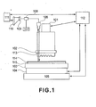
- Figure 1 shows the constitutional example of the imprint apparatus in Embodiment 1.
- the imprint apparatus includes an exposure light source 101, a mold holding portion 102, a work holding portion 103, a work pressing mechanism 104, an in-plane moving mechanism 105, an optical system 106, a measurement light source 107, a beam splitter 108, a spectroscope 109, an image-pickup device 110, an analyzer 111, an imprint control mechanism 112, a mold 113, a photo-curable resin material 114, and a substrate 115.
- the mold holding portion 102 effects chucking of the mold 113 by a vacuum chuck method or the like.
- a work or workpiece is movable to a desired position by the in-plane moving mechanism 105.
- the work pressing mechanism 104 is capable of adjusting a height of the work and applying pressure to the work.
- a position of the work pressing mechanism 104 in a height direction can be monitored by an encoder.
- the encoder may desirably have accuracy of 100 nm or below. Control of the position movement, pressure application, and light exposure with respect to the work is effected by the imprint control mechanism 112.
- the imprint apparatus can also include a detection system for effecting in-plane alignment (not shown).
- the substrate 115 is disposed at a position opposite to the mold 113 and onto the substrate 115, the photo-curable resin material 114 is applied.
- a material for a member onto which a pattern of the mold is to be transferred it is not limited to the photocurable resin material but may also be thermosetting resin materials, organic SOG (system on glass) materials, inorganic SOG materials, etc.
- the gap measuring mechanism in this embodiment includes the optical system 106, the measurement light source 107, the beam splitter 108, the spectroscope 109, the image pickup device 110, and the analyzer 111.
- the measurement light source 107 is constituted by a light source which emits broadband light of, e.g., 400 nm - 800 nm.
- the light emitted from the measurement light source 107 passes through the optical system 106 to reach the mold 113, the photo-curable resin material 114, and the substrate 115.
- the light interferes among the mold 113, the photocurable resin material 114, and the substrate 115.
- the interfering light is then returned to the optical system 106 to reach the spectroscope 109.
- the light dispersed by the spectroscope 109 is observed through the image pickup device 110 such as a line sensor.
- the analyzer 111 includes a storing device for storing refractive index and measured data in advance and performs processing of signal from the image pickup device.
- the optical system by providing an additional beam splitter to the optical system, it is also possible to branch the optical system into an optical system for effecting gap measurement and an optical system for effecting in-plane alignment (positional adjustment). As a result, the in-plane alignment and the gap measurement can be effected independently by less optical system.
- a light source there are a laser, an LED, etc. Further, it is also possible to use a broadband light source provided with a filter.
- a thin film has a thickness of d and a refractive index of n
- the case where light reflected at both end surfaces of the thin film is considered.
- a wave number k mo and a wavelength ⁇ mo are represented by the following relationship using any integer m.
- the light intensity is periodically changed depending on the wave number and the wavelength, so that it is periodically changed for each distance corresponding to half of the wavelength.
- a measurement wavelength is 600 nm and the refractive index n is 1.5
- a period of the change in light intensity is 200 nm.
- an encoder having an accuracy of approximately 100 nm. Further, when the sum of errors in initial position of a mold surface and a substrate surface is within 100 nm, it is possible to measure an absolute distance between the mold and the substrate.
- the broadband light source it is possible to use a halogen light source, a xenon light source, etc.
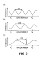
- Figures 2(a) to 2(c) are schematic views showing relationships between the wave number and the light intensity when respective refractive indices and respective film thicknesses are different from each other.
- Figure 2(a) shows a state in which there are three peaks and three valleys in a measurement wave number (range).
- Figure 2(b) shows a state in which there are two peaks and two valleys in the measurement wave number.
- Figure 2(c) shows a state in which there are a single peak and a single valley in the measurement wave number.
- the films in Figures 2(a) to 2(c) have refractive indices n a , n b and n c , respectively, and thicknesses d a , d b and d c , respectively.
- reference numerals 201 and 202 represent distances between adjacent peaks and are 1/2n a d a and 1/2n b d b , respectively.
- a reference numeral 203 represents a distance between adjacent peak and valley and is 1/4n c d c . Based on these values, it is possible to calculate an optical length (distance) nd by a frequency analysis such as Fourier transform and peak detection with respect to peak and valley or peak and peak.
- the refractive index does not depend on the wavelength for simplicity of explanation. An influence of multiple reflection such that light passed through an upper end is reflected at a lower end and then again reflected at the upper end and the lower end to be come out of the film is also not considered.
- d a 800 nm
- d b 500 nm
- d c 300 nm
- n 1.4
- k L 1/400
- k M 1/800
- the measurable minimum thickness is 71 nm.
- peaks are generated at three positions n a d a , n b d b , and n a d a + n b d b .
- peaks appear at six positions n a d a , n b d b , n c d c , n a d a + n b d b , n b d b + n c d c , and n a d a + n b d b + n c d c .
- optical interferometry is used as the measuring method but it is also possible to use a method using ellipsometry.
- changes in polarization state of incident light and reflected light are observed to obtain the film thickness, the distance between the mold and the substrate, etc.
- a condition of application to this method is that an optical length from the back surface of the mold to the front surface of the substrate is shorter than a coherence length of light.
- the optical length is longer than the coherence length, lights reflected at the back surface of the mold and the front surface of the substrate do not interfere with each other, thus being unmeasurable.
- the coherence length is 16 mm.
- the mold thickness is smaller than the coherence length, thus permitting measurement of the gap (distance between the mold and the substrate).
- Figure 3(a) is a schematic view showing a state in which the mold and the resin material do not contact each other.
- broadband light enters the mold and is reflected at a back surface 301 of the mold, a first surface 302 of the mold, a resin material surface 303, and a substrate surface 304.
- the respective reflected lights interference with each other as indicated by a reference numeral 305 and is returned to a measuring system.
- a distance between the back surface of the mold and the first surface of the mold (where a pattern is formed) is taken as d 1
- a distance between the first substrate of the mold and the resin material surface is taken as d 2
- a distance between the resin material surface and the substrate surface is taken as d 3 .
- these refractive indices may be stored in a memory of the imprint apparatus in advance and may appropriately be referenced.
- Figure 3(b) is a schematic view showing a state in which the mold and the resin material contact each other.
- the thickness of the mold is measured and stored. Then, the mold is brought near to the substrate by the wavelength pressing mechanism. Monitoring of the distance between the mold and the substrate is effected by an encoder of the wavelength pressing mechanism. When the mold is brought further near the substrate, the mold is placed in contact with the substrate. In this contact state, a peak appears at the position n 1 d 1 + n 3 d 3 .
- an optical axis subjected to measurement of n 1 d 1 in advance is identical to an optical axis subjected to measurement of distance during the approach of the mold to the substrate. For this reason, the distance between the pattern-formed substrate and the substrate surface can be determined with high accuracy.
- the distance between the pattern-formed substrate and the substrate surface can be controlled with high accuracy, it is also possible to control a thickness of a residual film layer, formed of the resin material on the substrate, with high accuracy. As a result, it is also possible to improve a precision of pattern transfer onto the substrate in a subsequent etching process.
- the value of refractive index of a material constituting the mold surface is close to that of refractive index of the resin material, when the mold and the resin material contact each other, it is difficult to obtain reflection spectrum from a boundary surface therebetween. For this reason, in the conventional method wherein the mold back surface or the like is not subjected to measurement, it is difficult to measure the distance between the pattern-formed surface and the substrate surface. In this embodiment, however, the back surface of the mold is also subjected to measurement, so that the distance between the mold surface and the substrate surface can be measured even in the case where the mold and the substrate contact each other.
- the intensity spectrum of the light source is not flat, it is also preferable that the intensity spectrum is measured in advance and normalization is effected by performing division between the spectrum of measurement light and the intensity spectrum. As a result, it is possible to effect frequency analysis with further high accuracy.
- the gap measuring mechanism is provided at three or more portions. As a result, an inclination between the mold and the substrate can be detected, so that it is also possible to adjust parallelism between the mold and the substrate.
- a driving mechanism for driving the optical system in an in-plane direction As another method for adjusting the parallelism between the mold and the substrate, it is also preferable that a driving mechanism for driving the optical system in an in-plane direction. As a result, it is possible to measure the gap while moving the measurement light in the in-plane direction. For example by measuring the gap at an origin point, a point moved in X-direction, and a point moved in Y-direction, inclination between the mold and the substrate can be detected. As a result, it is possible to adjust the parallelism.
- a first member 401 constitutes a body of the mold and is formed of a transparent material such as quartz glass (n: nearly equal to 1.5) or sapphire (n: nearly equal to 1.8).
- Figures 4(a) shows a mold constitution using a mold front surface 402 and a mold back surface 403 as a measurement surface.
- a rectangular area 406 is a measurement area subjected to measurement.
- Figure 4(b) shows a mold constitution using, as a measurement surface, a surface 405 located between the mold front surface 402 and the mold back surface 403 in place of the mold back surface 403.
- a rectangular area 406 is the measurement area subjected to measurement. This constitution is effective in the case where the distance between the pattern-formed surface 402 and the mold back surface 403 is longer than the coherence length. In this case, however, a distance between the pattern-formed surface 402 and the surface 405 is required to be shorter than the coherence length.
- Figure 4(c) shows another embodiment of Figure 4(b) a rectangular measurement area 406 is located at a recessed portion.
- the mold front surface, the mold back surface 403, and the surface 405 may desirably be a flat surface.
- Embodiment 2 a mold using a boundary surface between two members as the measurement surface and a measuring method using the mold will be described. This embodiment is useful in that it is applicable to even the case where the coherence length is shorter than the mold thickness.
- Figure 5(a) shows a mold constitution using, as the measurement surface, the boundary surface between two members.
- This mold is constituted by a first member 401 and a second mold 407.
- the boundary surface between these first and second member 401 and 407 is indicated by a reference numeral 408.
- the first member 401, the second member 407, and a photocurable resin material are constituted by materials different in refractive index.
- the second member 407 As a material for the second member 407, it is possible to use titanium oxide (n: nearly equal to 2.4), ITO (n: nearly equal to 2), silicon nitride (n: nearly equal to 2), etc. Further, the thickness of the second member 407 may desirably be 1/4 or more of a measurement wavelength in terms of the optical length.
- Figure 5(b) shown another embodiment of Figure 5(a) .
- this embodiment not only a projection but also a portion adjacent to the projection are formed of the second member 407.
- the boundary surface between the first member 401 and the second member 407 may desirably be a flat surface.
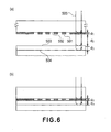
- Figure 6(a) shows a state in which the mold and the resin material do not contact each other.
- Surfaces shown in Figure 6(a) include a mold surface 501, a boundary surface 502 between the first member and the second member, a resin material surface 503, and a substrate surface 504. Broadband light entering the mold is reflected at the boundary surface 502, the resin material surface 503, and the substrate surface 504 and respective reflected lights interfere with each other and returned to the measuring system.
- the distance between the mold surface 501 and the boundary surface 502 is taken as d 1
- the distance between the mold surface 501 and the resin material surface 503 is taken as d 2
- the distance between the resin material surface 503 and the substrate surface is taken as d 3 .
- peaks appear at six positions n 1 d 1 , n 2 d 2 , n 3 d 3 , n 1 d 1 + n 2 d 2 , n 2 d 2 + n 3 d 3 , and n 1 d 1 + n 2 d 2 + n 3 d 3 .
- d 1 , d 2 and d 3 the distance between the pattern-formed surface and the substrate surface is d 2 +d 3 .
- Figure 6(b) shows a state in which the mold and the resin material contact each other.
- the mold and the resin material are different in refractive index
- reflection is caused to occur also at a boundary surface between the mold surface and the substrate surface. Accordingly, a peak appears at a position n 1 d 1 + n 3 d 3 . From this value, by subtracting the preliminarily measured n 1 d 1 , it is possible to calculate d 3 . As a result, it is possible to determine the distance between the pattern-formed surface and the substrate surface.
- Embodiment 1 description such that the mold thickness is measured by utilizing the mold back surface as the measurement surface, in the case where the coherence length of broadband light is longer than the mold thickness, to calculate the distance between the mold surface and the substrate surface is made.
- Embodiment 3 a measuring method having solved such a problem will be described.
- Figure 7(a) is a schematic view showing a noncontact state of the mold with the resin material.
- the broadband light entering the mold is reflected at a mold back surface 601, a mold front surface 602, a resin material surface 603, and a substrate surface 604. Respective reflected lights interfere with each other as indicated by a reference numeral 605 and are returned to the measuring system.
- Figure 7(b) is a schematic view showing a contact state of the mold with the resin material.
- the light entering the mold is changed from the broadband light to laser light.
- the laser light has a longer coherent length. For this reason, in the case where the distance between the mold back surface and the substrate surface is shorter than the coherence length of the laser light, the laser light is reflected at the mold back surface 601 and the substrate surface 604 and respective reflected lights interference with each other as indicated by a reference numeral 606.
- an intensity of the interfering light is changed sinusoidally. More specifically, when a wavelength of the laser light is taken as ⁇ , a period of the laser light is ⁇ /2n. Accordingly, it is possible to measure a movement distance L by counting the intensity of frequency and the number of peaks of intensity. By effecting the measurement as described above, the distance between the mold surface and the substrate surface can be calculated by the formula: dc - L.
- the change from the broadband light to the laser light is effected during the contact of the mold surface with the resin material but may also be effected before the contact with the resin material.
- the imprint method in this embodiment is characterized by a first measuring step of measuring the distance between the mold surface and the substrate surface by effecting irradiation with light of a first band, a second measuring step of measuring a movement distance of the mold by changing the irradiation light from the light of the first band to light of a second band narrower than the first band and effecting irradiation with the light of the second band, and a step of calculating the distance between the mold surface and the substrate surface by subtracting the distance measured in the second measuring step from the distance measured in the first measuring step.
- the imprint apparatus in this embodiment includes a first light source which is used for measuring the distance between the mold surface and the substrate surface and has a first band, a second light source having a second band narrower than the first band, an optical system for guiding the lights from the first light source and the second light source to the mold surface and the substrate surface and guiding the reflected lights to a spectroscope, the spectroscope for dispersing the light guided by the optical system, and an analyzer for analyzing the distance between the mold surface and the substrate surface.
- the analyzer is characterized in that the distance between the mold substrate and the substrate surface is calculated from the distance between the mold surface and the substrate surface obtained by effecting the irradiation using the first light source and the movement distance of the mold obtained by effecting the irradiation using the second light source.
- Embodiment 4 a constitutional embodiment in which a part of optical system for effecting distance measurement (Z) between the mold surface and the substrate surface and in-plane position measurement (XY ⁇ ) is coaxially disposed will be described.
- Figure 9(a) shows the optical system in this embodiment.
- Light emitted from a light source 802 passes through a first beam splitter 809 and first imaging optics 805 to reach a mold 806 and a substrate 807.
- the light reflected by the mold and the substrate is returned to the first imaging optics 805.
- the light passing through the first beam splitter 809 to reach a second beam splitter 808 is branched off in directions toward a light-condensing portion 803 for distance measurement and an image-pickup device 801 for in-plane position measurement, respectively.
- the light having reached the light-condensing portion 803 reaches a spectroscope 810 through a waveguide such as fibers or the like.
- the image-pickup device 801 and the light-condensing portion 803 are located at positions where information in the neighborhood of a focus of the first imaging optics 805 is formed into an image.
- an optical axis 804 from the substrate 807 to the second beam splitter 808 is shared by the distance measuring system and the in-plane position measuring system.
- the nanoimprint is a method in which the mold and a processing pattern have a size ratio of 1:1. For this reason, there is a limiting factor such that it is difficult to sufficiently ensure a space behind the back surface of the mold.
- the optical system for effecting the distance measurement and the optical system for effecting the in-plane position measurement are separately prepared, it is difficult to not only dispose these optical systems together behind the back surface of the mold but also effect the distance measurement and the in-plane position measurement simultaneously. In such a state, it is difficult to prevent an error in distance measurement by positional deviation between the mold and the substrate due to temperature change, vibration, etc.
- the optical system is shared, so that the above described limiting factor can be obviated.
- Figure 9(b) shows a constitution for changing a numerical aperture (NA) of the distance measuring system and NA of the in-plane position measuring system.
- This constitution includes a diaphragm 811 disposed between the second beam splitter 808 and the light-condensing portion 803.
- NA numerical aperture
- a larger NA provides a higher resolution and higher accuracy of position measurement.
- a smaller NA can be advantageous for removing an influence of aberration.
- the constitution of this embodiment is effective.
- Figure 9(c) shows a constitution for changing an optical magnification of the distance measuring system and an optical magnification of the in-plane position measuring system.
- a second imaging optics 812 is disposed between the second beam splitter 808 and the image-pickup device 801.
- a higher magnification can permit position measurement with higher accuracy.
- the distance measuring system has a small NA and less optical system in order to remove the influence of aberration. In this case, the constitution of this embodiment is effective.
- Figure 9(d) shows a constitution for effecting measurement of an inclination between the mold surface and the substrate surface.
- a driving mechanism 813 for moving the light-condensing portion 803 in a planar direction perpendicular to the optical axis is disposed at an image forming position.
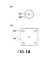
- the light-condensing portion 803 is constituted by a fiber 901 and a holding member 802.
- a reflection prevention film for suppressing unnecessary reflection may also be provided.
- a shape of the holding member 902 may also be a tapered shape so as not to return the light to the measuring portion.
- Figure 10(b) shows a member 904 provided with a plurality of openings 903.
- the member provided with the plurality of openings at an image surface is disposed between the light-condensing portion 803 and the second beam splitter 808 shown in Figure 9(a) .
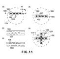
- a spatial position measurement mark area for simultaneously performing the distance measurement between the mold surface and the substrate surface and the in-plane position measurement will be described.
- a positive direction of z-axis is taken in a direction on the drawing from a back side to a front side as shown in Figure 11(a) .
- a circular area 1004 indicated by broken line is a field of view observed through the optical system.
- Figure 11(a) is a schematic view showing a state in which the mold and the substrate are located at substantially desired opposite positions.
- the spatial position measurement mark area is constituted by a first distance measurement area 1003 and an in-plane position measurement area 1005.
- the first distance measurement area 1003 corresponds to a central position of the field of view of the optical system.
- a plurality of mold mark constituting elements 1001 and a plurality of substrate mark constituting elements 1002 are disposed in the in-plane position measurement area 1005.
- the plurality of mold mark constituting elements 1001 is arranged in x-direction and the plurality of substrate mark constituting elements is arranged between adjacent mold mark constituting elements.
- Figure 11(b) is a sectional view taken along AA'-line shown in Figure 11(a) .
- a mold mark is constituted by a constitutional element 1006 having a projection structure and a substrate mark is constituted by a constitutional element 1007 having a recess structure.
- the mold surface is at the same level as a top surface of projection structure of mark and the substrate surface is at the same level as a top surface of projection structure of mark, so that a boundary area is not particularly provided.
- Figure 11(c) is another sectional view taken along AA'-line shown in Figure 11(a) , wherein the projection structure of the mold and the recess structure of the substrate are in reverse relationship with respect to the case of Figure 11(b) .
- both of these structures may be projection structures or recess structures.
- both of or either one of the mold mark and the substrate mark may also have a recess structure.
- Figure 11(d) shows a constitution in which a second distance measurement area 1010 and a part of an in-plane position measurement area 1005 overlap each other.
- Figure 11(e) shows a constitution of marks capable of effecting three-dimensional in-plane position measurement. According to this constitution, the distance measurement can be effected at the center of field of view on three axes. Further, by effecting the distance measurement at a peripheral portion 1011, it is possible to measure an inclination between the mold surface and the substrate surface.
- Figure 12(a) is a flowchart showing a sequence of in-plane position control and distance control using the mark constitutions shown in Figures 11(a) and 11(d) .
- Figure 12(a) is a flowchart showing a sequence of in-plane position control and distance control using the mark constitutions shown in Figures 11(a) and 11(d) .
- a combination of the mark and the optical system is provided at two or more positions.
- step S1-1 the mold is brought near to the substrate.
- a distance between a mold processing surface and a substrate surface is set to, e.g., approximately several tens of micrometers by coarse adjustment using an encoder or the like of a motor.
- step S1-2 a mark is selected.
- step S1-3 distance measurement is effected and in step S1-4, determination as to whether condition (1) is satisfied or not is made.
- the condition (1) is, e.g., such that an error in distance with respect to a desired distance is within several nanometers.
- distance control is effected in step S1-5.
- in-plane position measurement is effected in step S1-6.
- step S1-7 determination as to whether condition (2) is satisfied or not is made.
- the condition (2) is, e.g., such that an error in position is within several nanometers.
- in-plane position control is effected in step S1-8.
- determination of condition (2) is made in step S1-9.
- the condition (3) includes, e.g., (a) all the marks are not measured (b) as a result of measurement of all the marks, it is necessary to further bring the mold near to the substrate, and (c) as a result of measurement of all the marks, the distance between the mold processing surface and the substrate reaches a final value.
- the sequence goes to step S1-2 in which measurement of another mark is effected.
- step S1-10 the sequence goes to step S1-10 in which the distance between the mold processing surface and the substrate surface is decreased by slight movement so that the decrease in distance is several tens of nm to several hundreds of nm.
- step S1-10 the sequence is completed.
- Figure 12(b) is a flowchart showing a sequence in which three-dimensional positional alignment is effected by a single mark and a single optical system.
- step S2-1 similarly as in the case of Figure 12(a) , the mold is brought near to the substrate by movement (1).
- step S2-2 a distance therebetween is measured. This distance measurement is effected at a plurality of positions.
- step S2-3, an inclination between the mold processing surface and the substrate surface is calculated.
- step S2-4 determination of condition (1) such that errors in distance and inclination are within several nanometers is made.
- step S2-5 distance control is effected in step S2-5.
- step S2-6 determination of condition (2) such that an error in in-plane position is within several nanometers is made.
- step S2-8 in-plane position control is effected in step S2-8.
- determination of condition (3) is made in step S2-9.
- the condition (3) is whether or not the distance between the mold processing surface and the substrate surface is a final distance.
- the sequence is completed.
- the condition (3) is not satisfied, the sequence goes to step S2-11 in which the distance between the mold processing surface and the substrate surface is decreased.
- an imprint apparatus an imprint method, and a mold for imprint which are capable of more accurately measuring the distance between the mold surface and the substrate surface.
Landscapes
- Engineering & Computer Science (AREA)
- Physics & Mathematics (AREA)
- Nanotechnology (AREA)
- Chemical & Material Sciences (AREA)
- General Physics & Mathematics (AREA)
- Crystallography & Structural Chemistry (AREA)
- Mathematical Physics (AREA)
- Manufacturing & Machinery (AREA)
- Condensed Matter Physics & Semiconductors (AREA)
- Theoretical Computer Science (AREA)
- Health & Medical Sciences (AREA)
- Toxicology (AREA)
- Oral & Maxillofacial Surgery (AREA)
- Thermal Sciences (AREA)
- Shaping Of Tube Ends By Bending Or Straightening (AREA)
- Exposure Of Semiconductors, Excluding Electron Or Ion Beam Exposure (AREA)
- Length Measuring Devices By Optical Means (AREA)
Applications Claiming Priority (3)
| Application Number | Priority Date | Filing Date | Title |
|---|---|---|---|
| JP2005302679 | 2005-10-18 | ||
| JP2006230222A JP5268239B2 (ja) | 2005-10-18 | 2006-08-28 | パターン形成装置、パターン形成方法 |
| EP06812158A EP1941323A2 (fr) | 2005-10-18 | 2006-10-18 | Appareil d'empreinte, procede d'empreinte et moule d'empreinte |
Related Parent Applications (1)
| Application Number | Title | Priority Date | Filing Date |
|---|---|---|---|
| EP06812158A Division EP1941323A2 (fr) | 2005-10-18 | 2006-10-18 | Appareil d'empreinte, procede d'empreinte et moule d'empreinte |
Publications (2)
| Publication Number | Publication Date |
|---|---|
| EP2090928A2 true EP2090928A2 (fr) | 2009-08-19 |
| EP2090928A3 EP2090928A3 (fr) | 2009-11-04 |
Family
ID=37890191
Family Applications (2)
| Application Number | Title | Priority Date | Filing Date |
|---|---|---|---|
| EP06812158A Withdrawn EP1941323A2 (fr) | 2005-10-18 | 2006-10-18 | Appareil d'empreinte, procede d'empreinte et moule d'empreinte |
| EP09159207A Withdrawn EP2090928A3 (fr) | 2005-10-18 | 2006-10-18 | Appareil d'impression, procédé d'impression et moule pour impression |
Family Applications Before (1)
| Application Number | Title | Priority Date | Filing Date |
|---|---|---|---|
| EP06812158A Withdrawn EP1941323A2 (fr) | 2005-10-18 | 2006-10-18 | Appareil d'empreinte, procede d'empreinte et moule d'empreinte |
Country Status (5)
| Country | Link |
|---|---|
| US (2) | US8047828B2 (fr) |
| EP (2) | EP1941323A2 (fr) |
| JP (1) | JP5268239B2 (fr) |
| KR (1) | KR20080053503A (fr) |
| WO (1) | WO2007046528A2 (fr) |
Families Citing this family (31)
| Publication number | Priority date | Publication date | Assignee | Title |
|---|---|---|---|---|
| US9573319B2 (en) | 2007-02-06 | 2017-02-21 | Canon Kabushiki Kaisha | Imprinting method and process for producing a member in which a mold contacts a pattern forming layer |
| KR100931610B1 (ko) | 2008-01-30 | 2009-12-14 | 주식회사 에이디피엔지니어링 | 미세 패턴 임프린트 공정용 스탬프 및 기판 분리 장치 및방법 |
| JP5327421B2 (ja) * | 2008-03-14 | 2013-10-30 | 大日本印刷株式会社 | インプリント用スタンパ |
| IT1391719B1 (it) * | 2008-11-17 | 2012-01-27 | Marposs Spa | Metodo, stazione ed apparecchiatura per la misura ottica mediante interferometria dello spessore di un oggetto |
| NL2003871A (en) * | 2009-02-04 | 2010-08-05 | Asml Netherlands Bv | Imprint lithography. |
| JP5377053B2 (ja) * | 2009-04-17 | 2013-12-25 | 株式会社東芝 | テンプレート及びその製造方法、並びにパターン形成方法 |
| JP5284212B2 (ja) * | 2009-07-29 | 2013-09-11 | 株式会社東芝 | 半導体装置の製造方法 |
| MY172009A (en) | 2009-10-16 | 2019-11-11 | Alcon Inc | Process for manufacturing an ophthalmic lens |
| JP5419634B2 (ja) * | 2009-10-26 | 2014-02-19 | 株式会社東芝 | パターン形成方法 |
| WO2012028166A1 (fr) * | 2010-09-03 | 2012-03-08 | Ev Group E. Thallner Gmbh | Dispositif et procédé pour réduire une erreur de clavette |
| JP5637931B2 (ja) | 2011-05-17 | 2014-12-10 | キヤノン株式会社 | インプリント装置、インプリント方法およびデバイス製造方法 |
| JP5498448B2 (ja) | 2011-07-21 | 2014-05-21 | 株式会社東芝 | インプリント方法及びインプリントシステム |
| CN102346369B (zh) * | 2011-09-08 | 2013-04-10 | 青岛理工大学 | 一种整片晶圆纳米压印光刻机 |
| JP5824380B2 (ja) | 2012-02-07 | 2015-11-25 | キヤノン株式会社 | インプリント装置、インプリント方法、及び物品の製造方法 |
| JP6021365B2 (ja) * | 2012-03-12 | 2016-11-09 | キヤノン株式会社 | インプリント装置、それを用いた物品の製造方法 |
| US20140205702A1 (en) * | 2013-01-24 | 2014-07-24 | Kabushiki Kaisha Toshiba | Template, manufacturing method of the template, and position measuring method in the template |
| US20140209567A1 (en) * | 2013-01-29 | 2014-07-31 | Kabushiki Kaisha Toshiba | Template, manufacturing method of the template, and strain measuring method in the template |
| JPWO2015022851A1 (ja) * | 2013-08-15 | 2017-03-02 | 富士通株式会社 | 光干渉法を用いた計測装置及び光干渉法を用いた計測方法 |
| JP6361970B2 (ja) * | 2014-09-19 | 2018-07-25 | 大日本印刷株式会社 | ナノインプリント用構造体の検査方法およびその製造方法 |
| JP6552521B2 (ja) * | 2014-12-12 | 2019-07-31 | キヤノン株式会社 | インプリント装置、インプリント方法及び物品の製造方法 |
| JP6525628B2 (ja) * | 2015-02-13 | 2019-06-05 | キヤノン株式会社 | インプリント装置及び物品の製造方法 |
| JP6282298B2 (ja) * | 2015-06-10 | 2018-02-21 | キヤノン株式会社 | インプリント装置、インプリント方法、および物品の製造方法 |
| CN106335180B (zh) * | 2015-07-10 | 2018-08-17 | 李永春 | 数字式滚筒模仁制造系统 |
| US11298856B2 (en) * | 2017-03-16 | 2022-04-12 | Molecular Imprints, Inc. | Optical polymer films and methods for casting the same |
| EP3697588B1 (fr) | 2017-10-17 | 2024-04-03 | Magic Leap, Inc. | Un système pour mouler un matériau photodurcissable en un objet plan |
| JP6528994B2 (ja) * | 2018-07-02 | 2019-06-12 | 大日本印刷株式会社 | ナノインプリント用構造体の検査方法およびその製造方法 |
| US11009661B2 (en) | 2018-10-16 | 2021-05-18 | Magic Leap, Inc. | Methods and apparatuses for casting polymer products |
| JP2019176167A (ja) * | 2019-05-17 | 2019-10-10 | 大日本印刷株式会社 | ナノインプリント用構造体 |
| JP7558674B2 (ja) * | 2020-04-06 | 2024-10-01 | キヤノン株式会社 | インプリント装置、インプリント方法及び物品の製造方法 |
| JP7689539B2 (ja) | 2020-06-09 | 2025-06-06 | エーエスエムエル ホールディング エヌ.ブイ. | 内蔵同軸照明を備えたリソグラフィプリアライメント結像センサ |
| JP7646447B2 (ja) * | 2021-05-13 | 2025-03-17 | キヤノン株式会社 | 基板処理装置、基板処理方法、及び物品の製造方法 |
Family Cites Families (35)
| Publication number | Priority date | Publication date | Assignee | Title |
|---|---|---|---|---|
| IT1125000B (it) * | 1978-12-08 | 1986-05-14 | Rca Corp | Sistema automatico per l'allineamento di fotomaschere in processi di stampa a proiezione |
| US4422763A (en) | 1978-12-08 | 1983-12-27 | Rca Corporation | Automatic photomask alignment system for projection printing |
| NL9001611A (nl) * | 1990-07-16 | 1992-02-17 | Asm Lithography Bv | Apparaat voor het afbeelden van een maskerpatroon op een substraat. |
| US5414514A (en) * | 1993-06-01 | 1995-05-09 | Massachusetts Institute Of Technology | On-axis interferometric alignment of plates using the spatial phase of interference patterns |
| US5515167A (en) * | 1994-09-13 | 1996-05-07 | Hughes Aircraft Company | Transparent optical chuck incorporating optical monitoring |
| US5923033A (en) | 1994-09-14 | 1999-07-13 | Olympus Optical Co., Ltd. | Integrated SPM sensor having a photodetector mounted on a probe on a free end of a supported cantilever |
| CN1131741A (zh) | 1995-03-22 | 1996-09-25 | 载歌公司 | 光学间隙测量装置和方法 |
| JP3445100B2 (ja) * | 1997-06-02 | 2003-09-08 | キヤノン株式会社 | 位置検出方法及び位置検出装置 |
| US5991022A (en) * | 1997-12-09 | 1999-11-23 | N&K Technology, Inc. | Reflectance spectrophotometric apparatus with toroidal mirrors |
| US6541287B2 (en) * | 1998-03-19 | 2003-04-01 | Kabushiki Kaisha Toshiba | Temperature measuring method and apparatus, measuring method for the thickness of the formed film, measuring apparatus for the thickness of the formed film thermometer for wafers |
| JP2000193423A (ja) * | 1998-12-28 | 2000-07-14 | Tdk Corp | 膜厚測定方法、研磨方法及び薄膜磁気ヘッドの製造方法、並びに薄膜磁気ヘッド形成用基板 |
| WO2000072093A1 (fr) | 1999-05-25 | 2000-11-30 | Massachusetts Institute Of Technology | Appareil de mesure de l'intervalle optique et procede utilisant une marque a reseau optique a deux dimensions avec fluctuation unidirectionnelle de longueur d'onde |
| KR100862301B1 (ko) * | 2000-07-16 | 2008-10-13 | 보드 오브 리전츠, 더 유니버시티 오브 텍사스 시스템 | 임프린트 리소그래피를 위한 고분해능 오버레이 정렬 방법 및 시스템 |
| JP3638513B2 (ja) * | 2000-09-25 | 2005-04-13 | 株式会社東芝 | 転写装置及び転写方法 |
| EP1352295B1 (fr) * | 2000-10-12 | 2015-12-23 | Board of Regents, The University of Texas System | Gabarit pour photolithographie a temperature ambiante et basse pression produisant des empreintes de l'ordre du micron et du nanometre |
| EP1512048B1 (fr) * | 2001-05-16 | 2007-03-07 | Board Of Regents, The University Of Texas System | Procede de fabrication de motifs a nano-echelle dans des compositions durcissables a la lumiere au moyen d'un champ electrique |
| US6964793B2 (en) | 2002-05-16 | 2005-11-15 | Board Of Regents, The University Of Texas System | Method for fabricating nanoscale patterns in light curable compositions using an electric field |
| TW557368B (en) | 2001-06-29 | 2003-10-11 | Jsr Corp | Anti-reflection film laminated body and method of manufacturing the laminated body |
| JP3789089B2 (ja) | 2001-10-15 | 2006-06-21 | キヤノン株式会社 | 画像形成装置 |
| KR100438787B1 (ko) * | 2002-05-13 | 2004-07-05 | 삼성전자주식회사 | 박막 두께 측정 방법 |
| US6916584B2 (en) | 2002-08-01 | 2005-07-12 | Molecular Imprints, Inc. | Alignment methods for imprint lithography |
| US6916511B2 (en) * | 2002-10-24 | 2005-07-12 | Hewlett-Packard Development Company, L.P. | Method of hardening a nano-imprinting stamp |
| US6871558B2 (en) * | 2002-12-12 | 2005-03-29 | Molecular Imprints, Inc. | Method for determining characteristics of substrate employing fluid geometries |
| JP2004259985A (ja) * | 2003-02-26 | 2004-09-16 | Sony Corp | レジストパターン形成装置およびその形成方法、および、当該方法を用いた半導体装置の製造方法 |
| JP4061220B2 (ja) | 2003-03-20 | 2008-03-12 | 株式会社日立製作所 | ナノプリント装置、及び微細構造転写方法 |
| JP4217551B2 (ja) * | 2003-07-02 | 2009-02-04 | キヤノン株式会社 | 微細加工方法及び微細加工装置 |
| TWI226934B (en) | 2003-11-27 | 2005-01-21 | Hong Hocheng | System of nanoimprint with mold deformation detector and method of monitoring the same |
| JP2005208046A (ja) | 2003-12-25 | 2005-08-04 | Canon Inc | 反応性硬化樹脂の硬化状態測定装置及び方法 |
| JP4393244B2 (ja) * | 2004-03-29 | 2010-01-06 | キヤノン株式会社 | インプリント装置 |
| WO2005093737A1 (fr) * | 2004-03-29 | 2005-10-06 | Pioneer Corporation | Appareil de transfert de motif et procédé de transfert de moti |
| US7927090B2 (en) * | 2004-08-10 | 2011-04-19 | Asml Netherlands B.V. | Imprint lithographic apparatus, device manufacturing method and device manufactured thereby |
| FI20045295A7 (fi) | 2004-08-13 | 2006-02-14 | Avantone Oy | Embossauslaite ja menetelmä embossauslaitteen säätämiseksi |
| CA2579603A1 (fr) | 2004-09-08 | 2006-03-16 | Nil Technology Aps | Etampe de nano-impression souple |
| US8202075B2 (en) | 2005-08-12 | 2012-06-19 | Canon Kabushiki Kaisha | Imprint apparatus and imprint method |
| JP5002211B2 (ja) * | 2005-08-12 | 2012-08-15 | キヤノン株式会社 | インプリント装置およびインプリント方法 |
-
2006
- 2006-08-28 JP JP2006230222A patent/JP5268239B2/ja not_active Expired - Fee Related
- 2006-10-18 KR KR1020087009092A patent/KR20080053503A/ko not_active Ceased
- 2006-10-18 US US11/719,434 patent/US8047828B2/en not_active Expired - Fee Related
- 2006-10-18 EP EP06812158A patent/EP1941323A2/fr not_active Withdrawn
- 2006-10-18 EP EP09159207A patent/EP2090928A3/fr not_active Withdrawn
- 2006-10-18 WO PCT/JP2006/321187 patent/WO2007046528A2/fr not_active Ceased
-
2009
- 2009-07-27 US US12/509,996 patent/US8845318B2/en not_active Expired - Fee Related
Also Published As
| Publication number | Publication date |
|---|---|
| KR20080053503A (ko) | 2008-06-13 |
| EP2090928A3 (fr) | 2009-11-04 |
| US20090283938A1 (en) | 2009-11-19 |
| US20080099941A1 (en) | 2008-05-01 |
| EP1941323A2 (fr) | 2008-07-09 |
| US8845318B2 (en) | 2014-09-30 |
| WO2007046528B1 (fr) | 2007-08-30 |
| WO2007046528A3 (fr) | 2007-07-19 |
| WO2007046528A2 (fr) | 2007-04-26 |
| JP2007139752A (ja) | 2007-06-07 |
| JP5268239B2 (ja) | 2013-08-21 |
| US8047828B2 (en) | 2011-11-01 |
Similar Documents
| Publication | Publication Date | Title |
|---|---|---|
| US8845318B2 (en) | Imprint apparatus, imprint method, and mold for imprint | |
| US7884935B2 (en) | Pattern transfer apparatus, imprint apparatus, and pattern transfer method | |
| US8845317B2 (en) | Alignment method, imprint method, alignment apparatus, and position measurement method | |
| US7794222B2 (en) | Mold, pattern forming method, and pattern forming apparatus | |
| TWI418950B (zh) | 壓印微影術 | |
| KR101597387B1 (ko) | 검출기, 임프린트 장치 및 물품 제조 방법 | |
| US7531821B2 (en) | Imprint apparatus and imprint method including dual movable image pick-up device | |
| TWI522750B (zh) | 標記位置量測裝置及方法、微影裝置及器件製造方法 | |
| US20050037143A1 (en) | Imprint lithography with improved monitoring and control and apparatus therefor | |
| JP7414576B2 (ja) | 位置計測装置、重ね合わせ検査装置、位置計測方法、インプリント装置および物品の製造方法 | |
| CN101427185A (zh) | 对准方法、压印方法、对准设备和位置测量方法 | |
| WO2004114016A2 (fr) | Lithographie d'impression a surveillance et controle ameliores, et appareil associes | |
| US20090101037A1 (en) | Gap measuring method, imprint method, and imprint apparatus | |
| US20130221556A1 (en) | Detector, imprint apparatus and method of manufacturing article | |
| KR101573116B1 (ko) | 측정 장치, 임프린트 시스템, 측정 방법 및 디바이스 제조 방법 | |
| KR102605547B1 (ko) | 임프린트 장치 및 물품 제조 방법 | |
| JP2008008889A (ja) | ギャップ測定方法、インプリント方法、及びインプリント装置 | |
| US20070035056A1 (en) | Imprint apparatus and imprint method | |
| TWI460559B (zh) | 用於微影裝置之位階感測器配置、微影裝置及器件製造方法 | |
| CN101292195A (zh) | 压印装置、压印方法和压印模具 | |
| JP2017092294A (ja) | インプリント装置、型、および物品の製造方法 | |
| TWI383466B (zh) | An imprinting platform alignment and leveling measurement system |
Legal Events
| Date | Code | Title | Description |
|---|---|---|---|
| PUAI | Public reference made under article 153(3) epc to a published international application that has entered the european phase |
Free format text: ORIGINAL CODE: 0009012 |
|
| AC | Divisional application: reference to earlier application |
Ref document number: 1941323 Country of ref document: EP Kind code of ref document: P |
|
| AK | Designated contracting states |
Kind code of ref document: A2 Designated state(s): AT BE BG CH CY CZ DE DK EE ES FI FR GB GR HU IE IS IT LI LT LU LV MC NL PL PT RO SE SI SK TR |
|
| PUAL | Search report despatched |
Free format text: ORIGINAL CODE: 0009013 |
|
| AK | Designated contracting states |
Kind code of ref document: A3 Designated state(s): AT BE BG CH CY CZ DE DK EE ES FI FR GB GR HU IE IS IT LI LT LU LV MC NL PL PT RO SE SI SK TR |
|
| STAA | Information on the status of an ep patent application or granted ep patent |
Free format text: STATUS: THE APPLICATION HAS BEEN WITHDRAWN |
|
| 18W | Application withdrawn |
Effective date: 20100125 |