EP2090960A1 - Verfahren und Vorrichtung für Herstellung von Berührungsschnittstellen - Google Patents
Verfahren und Vorrichtung für Herstellung von Berührungsschnittstellen Download PDFInfo
- Publication number
- EP2090960A1 EP2090960A1 EP09001748A EP09001748A EP2090960A1 EP 2090960 A1 EP2090960 A1 EP 2090960A1 EP 09001748 A EP09001748 A EP 09001748A EP 09001748 A EP09001748 A EP 09001748A EP 2090960 A1 EP2090960 A1 EP 2090960A1
- Authority
- EP
- European Patent Office
- Prior art keywords
- voltage
- threshold
- generating
- interface
- electronic interface
- Prior art date
- Legal status (The legal status is an assumption and is not a legal conclusion. Google has not performed a legal analysis and makes no representation as to the accuracy of the status listed.)
- Withdrawn
Links
Images


Classifications
-
- G—PHYSICS
- G06—COMPUTING OR CALCULATING; COUNTING
- G06F—ELECTRIC DIGITAL DATA PROCESSING
- G06F1/00—Details not covered by groups G06F3/00 - G06F13/00 and G06F21/00
- G06F1/26—Power supply means, e.g. regulation thereof
- G06F1/32—Means for saving power
- G06F1/3203—Power management, i.e. event-based initiation of a power-saving mode
- G06F1/3234—Power saving characterised by the action undertaken
- G06F1/325—Power saving in peripheral device
- G06F1/3262—Power saving in digitizer or tablet
-
- G—PHYSICS
- G06—COMPUTING OR CALCULATING; COUNTING
- G06F—ELECTRIC DIGITAL DATA PROCESSING
- G06F1/00—Details not covered by groups G06F3/00 - G06F13/00 and G06F21/00
- G06F1/26—Power supply means, e.g. regulation thereof
- G06F1/32—Means for saving power
- G06F1/3203—Power management, i.e. event-based initiation of a power-saving mode
- G06F1/3206—Monitoring of events, devices or parameters that trigger a change in power modality
- G06F1/3215—Monitoring of peripheral devices
-
- G—PHYSICS
- G06—COMPUTING OR CALCULATING; COUNTING
- G06F—ELECTRIC DIGITAL DATA PROCESSING
- G06F1/00—Details not covered by groups G06F3/00 - G06F13/00 and G06F21/00
- G06F1/26—Power supply means, e.g. regulation thereof
- G06F1/32—Means for saving power
- G06F1/3203—Power management, i.e. event-based initiation of a power-saving mode
- G06F1/3234—Power saving characterised by the action undertaken
- G06F1/325—Power saving in peripheral device
- G06F1/3271—Power saving in keyboard
-
- Y—GENERAL TAGGING OF NEW TECHNOLOGICAL DEVELOPMENTS; GENERAL TAGGING OF CROSS-SECTIONAL TECHNOLOGIES SPANNING OVER SEVERAL SECTIONS OF THE IPC; TECHNICAL SUBJECTS COVERED BY FORMER USPC CROSS-REFERENCE ART COLLECTIONS [XRACs] AND DIGESTS
- Y02—TECHNOLOGIES OR APPLICATIONS FOR MITIGATION OR ADAPTATION AGAINST CLIMATE CHANGE
- Y02D—CLIMATE CHANGE MITIGATION TECHNOLOGIES IN INFORMATION AND COMMUNICATION TECHNOLOGIES [ICT], I.E. INFORMATION AND COMMUNICATION TECHNOLOGIES AIMING AT THE REDUCTION OF THEIR OWN ENERGY USE
- Y02D10/00—Energy efficient computing, e.g. low power processors, power management or thermal management
-
- Y—GENERAL TAGGING OF NEW TECHNOLOGICAL DEVELOPMENTS; GENERAL TAGGING OF CROSS-SECTIONAL TECHNOLOGIES SPANNING OVER SEVERAL SECTIONS OF THE IPC; TECHNICAL SUBJECTS COVERED BY FORMER USPC CROSS-REFERENCE ART COLLECTIONS [XRACs] AND DIGESTS
- Y02—TECHNOLOGIES OR APPLICATIONS FOR MITIGATION OR ADAPTATION AGAINST CLIMATE CHANGE
- Y02D—CLIMATE CHANGE MITIGATION TECHNOLOGIES IN INFORMATION AND COMMUNICATION TECHNOLOGIES [ICT], I.E. INFORMATION AND COMMUNICATION TECHNOLOGIES AIMING AT THE REDUCTION OF THEIR OWN ENERGY USE
- Y02D30/00—Reducing energy consumption in communication networks
- Y02D30/50—Reducing energy consumption in communication networks in wire-line communication networks, e.g. low power modes or reduced link rate
Definitions
- the present invention relates to a method and a device for interfacing touch. It applies, in particular, to guarantee the autonomy of electronic products with a human-machine interface (“HMI”) tactile not connected to a permanent power source.
- HMI human-machine interface
- the present invention aims to remedy these disadvantages.
- the present invention thus has the advantage that the idle consumption is only equal to the consumption of the electronic interface in standby, including the consumption of a central unit in standby.
- the effectiveness of the present invention resides in particular in the fact that its average consumption is extremely low. Indeed, the electronic interface is active substantially only during the duration of the support on a voltage generating means, in order to perform the actions to be performed. The rest of the time, the electronic interface is "asleep", the current consumed being a standby current.
- the electronic interface comprises at least one resistance bridge adapted to compare the voltage of at least one voltage generating means with a voltage corresponding to a relaxation detection limit value.
- the voltage generating means comprises a piezoelectric element.
- the device that is the subject of the present invention, as briefly described above, comprises a touch-sensitive voltage generation means of said keyboard.
- the pressing on each of the keys is thus operated in real time from the moment the key has been pressed.
- An action related to the key press lasts exactly the time the key is pressed.
- the electronic interface is adapted to detect the positive and negative fluctuations of the voltage across each means for generating a voltage respectively corresponding to supports and releases on the means for generating a voltage.
- the electronic interface is adapted to compare the voltage at the terminals of each means for generating a voltage with at least one upper threshold voltage, to detect the pressing of a key associated with a generation means. a voltage and with at least a lower threshold voltage, for detecting the release of said key.
- the binary signal corresponding to the result of these two comparisons takes a predetermined value during the duration of the support maintained on the means for generating a voltage.
- the electronic interface comprises at least one voltage comparison means and a means for modifying the threshold voltage at which said voltage comparison means compares the voltage across a means for generating a voltage. voltage.
- a single means of comparing voltages makes it possible to detect the positive and negative fluctuations of the voltage at the terminals of a voltage generating means.
- the means for modifying the threshold voltage is adapted to lower the threshold voltage when it has been exceeded by the voltage at the terminals of the means for generating a voltage.
- said electronic interface comprises at least one voltage comparison means adapted to compare a voltage across each voltage generating means with a threshold voltage, the electronic interface being in standby when said voltage is lower than said threshold voltage.
- the implementation of the present invention is thus particularly simple.
- the electronic interface comprises a central unit adapted to perform a different action when pressing and / or releasing each voltage generating means.
- the device that is the subject of the present invention thus makes it possible to control multiple actions or functions according to the key or keys on which a user presses.
- the present invention relates to a switch, characterized in that it comprises an interfacing device object of the present invention, as briefly described above.
- the present invention relates to a drive, characterized in that it comprises an interface device object of the present invention, as briefly described above.
- the present invention relates to a remote control, characterized in that it comprises an interfacing device object of the present invention, as briefly described above.
- the device 100 comprises, on the one hand, a keyboard 105 comprising keys 110 and voltage generation means 115 and, on the other hand, an electronic interface 120 comprising means for comparing voltages 125, a means 130 for modifying threshold voltages applied to the voltage comparison means 125 and a CPU card 135.
- the CPU card 135 includes a power supply 140.
- the CPU is, for example, microcontroller, digital signal processor or "DSP" (acronym for Digital Signal Processor ”) or element comprising a processor.
- DSP digital signal processor
- element comprising a processor.
- the voltage generating means 115 are adapted to generate a voltage when subjected to mechanical deformation.
- the voltage generating means 115 comprise piezoelectric elements mechanically associated with the keys of the keyboard in a manner known per se.
- the keyboard 105 consists of a slab made of several sandwich materials, including the materials of the piezoelectric elements. On the front of this keyboard 105 are drawn pictograms identifying the areas where the user must press. Under each pictogram, there is a piezoelectric element. This touch screen comes with a flexible sheet with two ground signals and piezoelectric signals. A connector makes it possible to make the electrical connection with these signals. It is observed that each key of the keyboard 105 is associated with a voltage generation means 115, a voltage comparison means 125 and an input of the central unit 135.
- the threshold voltage change means 130 provides the same threshold voltage to all voltage comparison means 125. However, in a variant, provision is made for means for modifying the threshold voltage per key of the keyboard 105. This variant applies, in particular, in the case where it is desired to detect, in parallel, the support on several different keys.
- Each voltage generating means 115 is loaded by a resistor 620 (see FIG. figure 6 ), the resulting voltage being supplied to the input "-" of a voltage comparing means 125, while the threshold voltage provided by the threshold voltage changing means 130 is applied to the "+" inputs of the means comparison of voltages 125.
- the outputs of all the voltage comparison means 125 are connected to interrupt inputs of a central unit 650, for example a processor element (see FIG. figure 6 ), of the card 135.
- a central unit 650 for example a processor element (see FIG. figure 6 ), of the card 135.
- the comparison means 125 compares the voltage across the piezoelectric elements 115 to the threshold voltage, the signal resulting from this comparison being a binary signal understandable by any central unit. In the embodiment described, this binary signal is “1" when the key is at rest and "0" while pressing the key.
- the voltage from the corresponding piezoelectric element 115 is applied to the input "-" of the voltage comparison means 125 while the threshold voltage provided by the modifying means 130 is applied to the "+” input of this voltage comparison means 125.
- the output of the voltage comparing means 125 connected at an interrupt input of the CPU, is "1".
- the central unit is in standby and can wake up as soon as this entry switches to "0".
- the modifying means 130 consists of a central unit, generally the same as previously described, and a resistor bridge (see figure 6 ) which receives a signal from the output "threshold variation" of the central unit.
- the voltage from the piezoelectric element 115 becomes greater than "upper threshold” and the output of the voltage comparison means switches to "0".
- the central unit wakes up and immediately switches an output line, called “threshold variation”, to "0" (this line is at "1", at rest). This line makes it possible to modify the threshold voltage applied by the modifying means 130 to the "+” inputs of the voltage comparison means 125, so that the voltage coming from the piezoelectric element 115 is greater than the threshold (ie "lower_level” ).
- the output of the voltage comparison means 125 remains at "0" as long as the release of the key has not been detected.
- the outputs of all the other voltage comparison means 125 also go to "0" at the time of switching of the threshold voltage, the voltages from the voltage generating means being all greater than “lower threshold”.
- the output of the voltage comparison means 125 corresponding to the pressed key 105 then returns to "1” and the central unit then immediately returns the line “threshold variation" to "1", to wait for a new support since the outputs of all the voltage comparison means 125 switch back to "1" at the time of switching from the threshold voltage to "higher_threshold".
- the electronic signal processing interface detects the release of a voltage generating means and goes to sleep following each release of each voltage generating means.
- the electronic signal processing interface detects the support and / or release of a generation means of voltage and goes to sleep after each pressing and / or release of each voltage generating means.
- comparator means of very low power voltages 125 such as the Maxim MAX9120 comparator (registered trademarks) whose standby current is 0.45 ⁇ A at three volts of supply voltage makes it possible, for example , switches (see figure 3 ) or dimmers (see figure 4 ) equipped with a touch interface that operates with a "CR2032" battery with a battery life of two years without battery replacement.
- the device which is the subject of the present invention implements a tactile keyboard comprising voltage generation means, preferably piezoelectric elements, in which a mechanical deformation generates an electrical voltage, and an electronic interface for processing the signal, very low consumption.
- voltage generation means preferably piezoelectric elements, in which a mechanical deformation generates an electrical voltage
- electronic interface for processing the signal, very low consumption. This low consumption is obtained on the one hand, by making the electronic interface go out of the standby state only when a piezoelectric element has been activated and returning it to a standby state as soon as this element is released and, d on the other hand, by using means for comparing low voltage voltages.
- the average consumption of this interface depends directly on the number of touch keys to be operated, because of the number of voltage comparison means that corresponds to this number of keys.
- the inventor has, for example, made an interface with at least five keys having a range of at least two years for a product operating with a single battery "CR2032" market.
- An advantage of the implementation of the present invention is that the idle consumption is only equal to the consumption of the electronic interface, including the consumption of the central unit idle.
- the central unit is woken up when the binary signal (corresponding to the piezoelectric key pressed) changes from "1" to "0".
- the consumption of the piezoelectric keyboard being zero.
- the electronic interface comprises at least one voltage comparing means adapted to compare a voltage across each voltage generating means with a threshold voltage, the electronic interface being in standby when the voltage at the terminals each voltage generating means is less than the threshold voltage.
- FIG. 2 the evolution of a signal 205 corresponding to the voltage across a piezoelectric element subjected to a support and then to a relaxation.
- An "upper threshold” value 210 and a “lower threshold” value 215 are also observed.
- reference voltage "Vref sensor” 225 is observed and a binary signal 220 represents the result of a comparison of the voltage represented. by the signal 205 with the threshold value 210 and, once this value has been exceeded, with the threshold value 215.
- the voltage at the terminals of a piezoelectric element is equal to "Vref sensor" in the absence of mechanical deformation on the corresponding key, or in the presence of a permanent mechanical deformation.
- the electronic interface detects the positive peak corresponding to the pressing of a key on the keyboard, when the voltage at the terminals of the voltage generating means is above “upper threshold”, then the negative peak corresponding to the release when this voltage passes. below “lower_level”.
- the binary signal at the output of the voltage comparison means is "0" during the duration of the sustain maintained on the key associated with the piezoelectric element as illustrated in FIG. figure 2 .
- the change of threshold voltage is made by the CPU card as soon as it leaves the standby state, that is to say as soon as a voltage comparing means 125 detects that the voltage across a piezoelectric element exceeds the value of "upper threshold”.
- the value of "lower_threshold” then becomes the reference voltage for all the voltage comparison means 125.
- the output of the corresponding voltage comparison means then switches to the level "0", when the voltage across the piezoelectric element crosses the value "upper_threshold".
- the central unit then wakes up immediately and controls the threshold voltage control signal to assign the value "lower_value”.
- the voltage at the terminals of the piezoelectric element becomes equal to "Vref sensor” while the key is held down, the value "Vref sensor” being greater than the new threshold voltage, " lower_level ".
- the output of the voltage comparison means therefore remains at level "0" and the central unit therefore remains awake and executes an action that has been programmed to press the key in question.
- the output signal of the corresponding voltage comparison means therefore goes to "1", which immediately switches the “threshold variation” control signal to "1" and causes the "upper threshold” value to be assigned to the threshold voltage.
- all the other voltage comparison means provide, again, the same output signal "1", each voltage across one of the piezoelectric elements being equal to “Vref sensor", or between “lower_reset” and “ upper_threshold ".
- the central unit then enters the standby state, thus minimizing the power consumption.
- a switch 305 comprising the device 100 illustrated in FIG. figure 1 .
- the pressing of a key 310 allows switching from one state to another of the switch.
- an inverter 405 comprising the device 100 illustrated in FIG. figure 1 .
- Pressing a "+" key 410 makes it possible to control the increase of a control signal, for example of light intensity.
- Pressing a "-" key 415 makes it possible to control the decrease of the control signal.
- a remote control 505 comprising the device 100 illustrated in figure 1 . Pressing keys 510 to 525 makes it possible to remotely control a remote device, for example an alarm, an electrical doorbell or motors of a home automation system.
- the device 100 is shown in broken lines because it is behind the front face of the switch, the dimmer or the remote control, respectively.
- the electronic interface 120 can be associated with the achievement of specific actions (such as the ignition of a light source or the variation of its control) during the maintenance of pressing a key 110 of the keyboard 105. also to associate these actions only with the signals of beginning of support and / or to release keys 110.
- the reference voltage of the piezoelectric elements 615 is constituted by a first resistance bridge 605 followed by an operational amplifier 630 mounted as a follower.
- a second resistor bridge 610 connected at its terminals to the output of the operational amplifier 630 and to the "threshold variation" threshold control from a central unit 650 provides the threshold voltage, "upper threshold” or “lower threshold”, to a voltage comparison means 640 which furthermore receives the voltage across the piezoelectric element 615.
- the output signal of the voltage comparator means 640 is connected to an interrupt input of the CPU 650
- the central unit 650 is connected to a radiofrequency communicating circuit 660 for transmitting radiocommunicating signals.
- the supply voltage, V is equal to 3.3 volts. Since the two resistors of the first resistor bridge 605 are equal, the reference voltage is 1.65 volts. The resistance of the second resistor bridge 610 connected to the reference voltage being equal to 7.5% of the resistance connected to the "threshold variation" output of the central unit 650, when the "threshold variation" signal has the logic value "1", that is to say is 3.3 Volts, the threshold voltage "upper threshold” is 1.77 Volts and when the signal “threshold variation” has the logic value "0", that is to say say, 0 volts, the threshold voltage "lower threshold” is 1.53 volts.
- the two dividing bridges consume, in total, 0.24 ⁇ A.
- a voltage comparison means consisting of a Maxim MAX9120 comparator (registered trademark), which consumes about 0.45 ⁇ A under 3V in standby mode and Maxim MAX4464 (registered trademark) operational amplifier consumes 0.75 ⁇ A under 3V.
- the current consumed, in standby is equal to (0.24 + N x 0.45 + 0.75) ⁇ A, to which must be added the current of consumption of a central unit in standby, ie less than 1 ⁇ A for a microcontroller.
- the means for modifying the threshold voltage at which the voltage comparing means 640 compares the voltage across a voltage generating means 615 consists of the resistor bridge 610, a point of which is connected to a binary output ( "Threshold variation") of the central unit 650, which confers two possible threshold voltage values.
- the comparison means are incorporated in the central unit 650. This avoids several components, which reduces the cost and the consumption of the device.
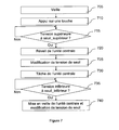
- a device object of the present invention is in an initial state of standby, during a step 705.
- a user presses a key on the keyboard of the device.
- step 715 it is determined whether the voltage at the terminals of each voltage generating means is greater than the "upper threshold" value. If no, we return to step 715. If yes, during a step 720, we wake up a CPU.
- the central unit modifies the threshold voltage that is compared with the voltage across the voltage generating means for which, during step 715, the crossing of the initial threshold voltage ("upper_threshold").
- the new threshold voltage has the value "lower_reset”.
- the central unit performs a task related to the key on which a support is made since step 710.
- the central unit modifies the state of a switch or a inverter for increasing or decreasing a signal, for example lighting control, a motor, an actuator, an electronic or computer system.
- step 735 it is determined whether the voltage at the terminals of each voltage generating means is lower than the value "lower_reset". If no, we return to step 730. If yes, during a step 740, we put the central unit in standby.
- the standby of the central unit is deferred by it, for example so that it finishes a task or stores useful parameter values for its next awakening.
- this when a user presses a key on the keyboard, this triggers an action after a defined duration.
- the central unit when awakened by an output signal from one of the means of comparison of tension, can decide to act immediately or wait.
- a user when a user presses a key, it triggers an action controlled by the central unit and an automatic standby of the central unit. In variants, only the pressing of a key or the release of the key is taken into account to perform an action. Only one threshold voltage value can then be implemented. In variants, when a user releases the key, this triggers a new action and a new standby. Two threshold voltages are then implemented and maintained during the standby phases.
- the present invention applies to all devices that may include a touch interface.
Landscapes
- Engineering & Computer Science (AREA)
- Theoretical Computer Science (AREA)
- Physics & Mathematics (AREA)
- General Engineering & Computer Science (AREA)
- General Physics & Mathematics (AREA)
- Input From Keyboards Or The Like (AREA)
- Push-Button Switches (AREA)
Applications Claiming Priority (1)
| Application Number | Priority Date | Filing Date | Title |
|---|---|---|---|
| FR0851029A FR2927710B1 (fr) | 2008-02-18 | 2008-02-18 | Procede et dispositif d'interfacage tactile |
Publications (1)
| Publication Number | Publication Date |
|---|---|
| EP2090960A1 true EP2090960A1 (de) | 2009-08-19 |
Family
ID=39777127
Family Applications (1)
| Application Number | Title | Priority Date | Filing Date |
|---|---|---|---|
| EP09001748A Withdrawn EP2090960A1 (de) | 2008-02-18 | 2009-02-09 | Verfahren und Vorrichtung für Herstellung von Berührungsschnittstellen |
Country Status (4)
| Country | Link |
|---|---|
| US (1) | US20090207147A1 (de) |
| EP (1) | EP2090960A1 (de) |
| CN (1) | CN101515202A (de) |
| FR (1) | FR2927710B1 (de) |
Families Citing this family (21)
| Publication number | Priority date | Publication date | Assignee | Title |
|---|---|---|---|---|
| CN102025814A (zh) * | 2009-09-11 | 2011-04-20 | 深圳富泰宏精密工业有限公司 | 便携式电子装置 |
| US8970507B2 (en) * | 2009-10-02 | 2015-03-03 | Blackberry Limited | Method of waking up and a portable electronic device configured to perform the same |
| EP2315102B1 (de) * | 2009-10-02 | 2018-01-31 | BlackBerry Limited | Niedrigleistungs-Aufweckdetektionsschaltung und tragbare elektronische Vorrichtung mit Niedrigleistungs-Aufweckdetektionsschaltung |
| EP2315101B1 (de) * | 2009-10-02 | 2014-01-29 | BlackBerry Limited | Verfahren zum Aufwecken und eine zur Durchführung des Verfahrens konfigurierte tragbare elektronische Vorrichtung |
| CA2779916C (en) | 2009-12-18 | 2015-02-10 | Honda Motor Co., Ltd. | Morphable pad for tactile control |
| WO2011099361A1 (ja) * | 2010-02-15 | 2011-08-18 | 京セラ株式会社 | 電子機器 |
| US8810105B2 (en) * | 2010-06-15 | 2014-08-19 | Aito B.V. | Apparatus and method for reducing energy consumption in monitoring means of a plurality of piezoelectric components |
| CN102467241B (zh) * | 2010-11-12 | 2015-01-07 | 珠海全志科技股份有限公司 | 移动终端的键盘及其实现按键和键盘锁定的方法 |
| US10817043B2 (en) * | 2011-07-26 | 2020-10-27 | Nvidia Corporation | System and method for entering and exiting sleep mode in a graphics subsystem |
| JP5874739B2 (ja) * | 2011-12-16 | 2016-03-02 | 株式会社村田製作所 | タッチ式操作入力装置 |
| CN104641327B (zh) | 2012-09-28 | 2017-06-23 | 株式会社村田制作所 | 按压量检测传感器、触摸式输入装置 |
| TWI486831B (zh) * | 2012-10-19 | 2015-06-01 | Elan Microelectronics Corp | 省電裝置及其省電方法 |
| JPWO2014196188A1 (ja) * | 2013-06-06 | 2017-02-23 | パナソニックIpマネジメント株式会社 | 物理量センサの調整方法および物理量センサ |
| KR101618272B1 (ko) * | 2014-11-25 | 2016-05-04 | 주식회사 이노칩테크놀로지 | 단말기 제어 장치 및 이를 이용한 제어 방법 |
| US10013025B2 (en) * | 2014-12-11 | 2018-07-03 | Intel Corporation | Wearable device with power state control |
| DE102015203921A1 (de) * | 2015-03-05 | 2016-09-08 | Tridonic Gmbh & Co Kg | Vorrichtung, System und Verfahren zum Erzeugen von Steuersignalen |
| ES2861520T3 (es) | 2016-04-12 | 2021-10-06 | E Vision Smart Optics Inc | Lentes electroactivas con puentes resistivos elevados |
| US10599006B2 (en) | 2016-04-12 | 2020-03-24 | E-Vision Smart Optics, Inc. | Electro-active lenses with raised resistive bridges |
| CN106059558B (zh) * | 2016-06-24 | 2019-07-09 | 苏州聚元微电子股份有限公司 | 解决触摸按键无法识别触摸动作的方法及其触摸识别系统 |
| KR102711838B1 (ko) * | 2016-12-01 | 2024-10-02 | 삼성전자주식회사 | 전자 장치 및 전자 장치 제어 방법 |
| US11009986B2 (en) * | 2017-07-21 | 2021-05-18 | Sony Corporation | Sensor and electronic device |
Citations (5)
| Publication number | Priority date | Publication date | Assignee | Title |
|---|---|---|---|---|
| US4511760A (en) * | 1983-05-23 | 1985-04-16 | International Business Machines Corporation | Force sensing data input device responding to the release of pressure force |
| JPH0546295A (ja) * | 1991-08-16 | 1993-02-26 | Toshiba Corp | 低消費電力キーボードシステム |
| US5669004A (en) * | 1994-09-07 | 1997-09-16 | Compaq Computer Corporation | Reducing power usage in a personal computer |
| JPH09319471A (ja) * | 1996-05-31 | 1997-12-12 | Nec Eng Ltd | 電子装置 |
| US6445383B1 (en) * | 1998-02-09 | 2002-09-03 | Koninklijke Philips Electronics N.V. | System to detect a power management system resume event from a stylus and touch screen |
Family Cites Families (6)
| Publication number | Priority date | Publication date | Assignee | Title |
|---|---|---|---|---|
| US6873863B2 (en) * | 2001-03-19 | 2005-03-29 | Nokia Mobile Phones Ltd. | Touch sensitive navigation surfaces for mobile telecommunication systems |
| US20030025721A1 (en) * | 2001-08-06 | 2003-02-06 | Joshua Clapper | Hand mounted ultrasonic position determining device and system |
| US20080007532A1 (en) * | 2006-07-05 | 2008-01-10 | E-Lead Electronic Co., Ltd. | Touch-sensitive pad capable of detecting depressing pressure |
| US8058937B2 (en) * | 2007-01-30 | 2011-11-15 | Cypress Semiconductor Corporation | Setting a discharge rate and a charge rate of a relaxation oscillator circuit |
| US20090002199A1 (en) * | 2007-06-28 | 2009-01-01 | Nokia Corporation | Piezoelectric sensing as user input means |
| US20100207890A1 (en) * | 2009-02-19 | 2010-08-19 | Ideacom Technology Corporation (Taiwan) | Singal detecting apparatus |
-
2008
- 2008-02-18 FR FR0851029A patent/FR2927710B1/fr active Active
-
2009
- 2009-02-09 EP EP09001748A patent/EP2090960A1/de not_active Withdrawn
- 2009-02-17 CN CNA2009100073800A patent/CN101515202A/zh active Pending
- 2009-03-27 US US12/372,885 patent/US20090207147A1/en not_active Abandoned
Patent Citations (5)
| Publication number | Priority date | Publication date | Assignee | Title |
|---|---|---|---|---|
| US4511760A (en) * | 1983-05-23 | 1985-04-16 | International Business Machines Corporation | Force sensing data input device responding to the release of pressure force |
| JPH0546295A (ja) * | 1991-08-16 | 1993-02-26 | Toshiba Corp | 低消費電力キーボードシステム |
| US5669004A (en) * | 1994-09-07 | 1997-09-16 | Compaq Computer Corporation | Reducing power usage in a personal computer |
| JPH09319471A (ja) * | 1996-05-31 | 1997-12-12 | Nec Eng Ltd | 電子装置 |
| US6445383B1 (en) * | 1998-02-09 | 2002-09-03 | Koninklijke Philips Electronics N.V. | System to detect a power management system resume event from a stylus and touch screen |
Also Published As
| Publication number | Publication date |
|---|---|
| CN101515202A (zh) | 2009-08-26 |
| FR2927710A1 (fr) | 2009-08-21 |
| US20090207147A1 (en) | 2009-08-20 |
| FR2927710B1 (fr) | 2011-04-15 |
Similar Documents
| Publication | Publication Date | Title |
|---|---|---|
| EP2090960A1 (de) | Verfahren und Vorrichtung für Herstellung von Berührungsschnittstellen | |
| US8436804B2 (en) | Digital photo frame with power saving function and related power saving method | |
| CN107885534B (zh) | 一种锁屏方法、终端及计算机可读介质 | |
| CA2761191C (en) | Portable electronic device with face touch detection | |
| US9733822B2 (en) | Electronic device and state controlling method | |
| CN106990888B (zh) | 一种应用显示控制方法及装置 | |
| TW201137826A (en) | Display device and method of controlling display device | |
| EP0682304B1 (de) | Mikrosystem mit niedrigem Energieverbrauch | |
| US10250736B2 (en) | Terminal controlling device and controlling method using same | |
| CN113472357A (zh) | 触摸按键扫描电路、低功耗模式退出方法及装置 | |
| US20170228094A1 (en) | Method and Device for Detecting Fascia Damage and Repairing the Same | |
| CN110989817B (zh) | 电子设备及电子设备开机管理方法 | |
| AU2017413665B2 (en) | Method and apparatus for quantifying button click force | |
| US20190073033A1 (en) | Electrical Haptic Output Array | |
| US10203786B1 (en) | Touch enabled user device with unpowered display | |
| CN108985258B (zh) | 光学式检测装置及其检测方法 | |
| TWI896862B (zh) | 電子裝置、用於觸發該電子裝置之功能的方法、及相關電腦程式 | |
| JP2021056987A (ja) | スマートデバイスの制御方法、スマートデバイスの制御装置、電子機器及び記憶媒体 | |
| EP3750037B1 (de) | System und verfahren zum filtern der steuerungen eines systems mit mehreren berührungsbildschirmen eines fahrzeugs | |
| EP1598675A1 (de) | Verfahren zur optimalen Batterieladungverwaltung eines Mobilkommunkationsendgerätes | |
| FR2846479A1 (fr) | Circuit permettant de detecter l'etat d'au moins un interrupteur electrique | |
| US9013407B2 (en) | Power-saving sensing module for optical mouse and power-saving sensing method | |
| JP2003298684A (ja) | 携帯電話装置の照明制御装置及びその再照明方法 | |
| FR2940847A1 (fr) | Dispositif d'interfacage tactile | |
| CA2297257A1 (fr) | Dispositif de gestion d'un clavier a touches |
Legal Events
| Date | Code | Title | Description |
|---|---|---|---|
| PUAI | Public reference made under article 153(3) epc to a published international application that has entered the european phase |
Free format text: ORIGINAL CODE: 0009012 |
|
| AK | Designated contracting states |
Kind code of ref document: A1 Designated state(s): AT BE BG CH CY CZ DE DK EE ES FI FR GB GR HR HU IE IS IT LI LT LU LV MC MK MT NL NO PL PT RO SE SI SK TR |
|
| AX | Request for extension of the european patent |
Extension state: AL BA RS |
|
| AKX | Designation fees paid | ||
| REG | Reference to a national code |
Ref country code: DE Ref legal event code: 8566 |
|
| STAA | Information on the status of an ep patent application or granted ep patent |
Free format text: STATUS: THE APPLICATION IS DEEMED TO BE WITHDRAWN |
|
| 18D | Application deemed to be withdrawn |
Effective date: 20100220 |