EP2091092A1 - Verfahren zur Erzeugung eines Nanokontakts in einem Spinventil, das in einen Funkoszillator eingebaut werden soll - Google Patents
Verfahren zur Erzeugung eines Nanokontakts in einem Spinventil, das in einen Funkoszillator eingebaut werden soll Download PDFInfo
- Publication number
- EP2091092A1 EP2091092A1 EP09305066A EP09305066A EP2091092A1 EP 2091092 A1 EP2091092 A1 EP 2091092A1 EP 09305066 A EP09305066 A EP 09305066A EP 09305066 A EP09305066 A EP 09305066A EP 2091092 A1 EP2091092 A1 EP 2091092A1
- Authority
- EP
- European Patent Office
- Prior art keywords
- layer
- nanocontact
- spin valve
- producing
- valve according
- Prior art date
- Legal status (The legal status is an assumption and is not a legal conclusion. Google has not performed a legal analysis and makes no representation as to the accuracy of the status listed.)
- Granted
Links
- 238000000034 method Methods 0.000 title claims description 25
- 230000005291 magnetic effect Effects 0.000 claims abstract description 42
- 238000005530 etching Methods 0.000 claims abstract description 35
- 238000000151 deposition Methods 0.000 claims abstract description 28
- 229910052751 metal Inorganic materials 0.000 claims abstract description 25
- 239000002184 metal Substances 0.000 claims abstract description 25
- 238000004519 manufacturing process Methods 0.000 claims abstract description 13
- 239000000470 constituent Substances 0.000 claims abstract description 9
- 230000004888 barrier function Effects 0.000 claims abstract description 4
- 230000008030 elimination Effects 0.000 claims abstract description 4
- 238000003379 elimination reaction Methods 0.000 claims abstract description 4
- 230000001939 inductive effect Effects 0.000 claims abstract description 3
- 239000010410 layer Substances 0.000 claims description 131
- 230000008021 deposition Effects 0.000 claims description 18
- 230000008569 process Effects 0.000 claims description 18
- 238000004544 sputter deposition Methods 0.000 claims description 14
- 230000005290 antiferromagnetic effect Effects 0.000 claims description 11
- 238000000231 atomic layer deposition Methods 0.000 claims description 9
- 238000005538 encapsulation Methods 0.000 claims description 8
- VYPSYNLAJGMNEJ-UHFFFAOYSA-N Silicium dioxide Chemical compound O=[Si]=O VYPSYNLAJGMNEJ-UHFFFAOYSA-N 0.000 claims description 7
- 229910052782 aluminium Inorganic materials 0.000 claims description 7
- XAGFODPZIPBFFR-UHFFFAOYSA-N aluminium Chemical compound [Al] XAGFODPZIPBFFR-UHFFFAOYSA-N 0.000 claims description 7
- 230000005415 magnetization Effects 0.000 claims description 7
- 239000000463 material Substances 0.000 claims description 7
- 238000000206 photolithography Methods 0.000 claims description 7
- 125000006850 spacer group Chemical group 0.000 claims description 7
- 238000001020 plasma etching Methods 0.000 claims description 6
- 239000011347 resin Substances 0.000 claims description 6
- 229920005989 resin Polymers 0.000 claims description 6
- 229910019041 PtMn Inorganic materials 0.000 claims description 5
- 229910045601 alloy Inorganic materials 0.000 claims description 5
- 239000000956 alloy Substances 0.000 claims description 5
- 239000002356 single layer Substances 0.000 claims description 5
- 229910018072 Al 2 O 3 Inorganic materials 0.000 claims description 4
- VYZAMTAEIAYCRO-UHFFFAOYSA-N Chromium Chemical compound [Cr] VYZAMTAEIAYCRO-UHFFFAOYSA-N 0.000 claims description 4
- PNEYBMLMFCGWSK-UHFFFAOYSA-N aluminium oxide Inorganic materials [O-2].[O-2].[O-2].[Al+3].[Al+3] PNEYBMLMFCGWSK-UHFFFAOYSA-N 0.000 claims description 4
- 229910052804 chromium Inorganic materials 0.000 claims description 4
- 239000011651 chromium Substances 0.000 claims description 4
- 238000010884 ion-beam technique Methods 0.000 claims description 4
- 229910015136 FeMn Inorganic materials 0.000 claims description 3
- ZOKXTWBITQBERF-UHFFFAOYSA-N Molybdenum Chemical compound [Mo] ZOKXTWBITQBERF-UHFFFAOYSA-N 0.000 claims description 3
- KJTLSVCANCCWHF-UHFFFAOYSA-N Ruthenium Chemical compound [Ru] KJTLSVCANCCWHF-UHFFFAOYSA-N 0.000 claims description 3
- RTAQQCXQSZGOHL-UHFFFAOYSA-N Titanium Chemical compound [Ti] RTAQQCXQSZGOHL-UHFFFAOYSA-N 0.000 claims description 3
- 229910052750 molybdenum Inorganic materials 0.000 claims description 3
- 239000011733 molybdenum Substances 0.000 claims description 3
- 229910052707 ruthenium Inorganic materials 0.000 claims description 3
- 239000000377 silicon dioxide Substances 0.000 claims description 3
- 229910052715 tantalum Inorganic materials 0.000 claims description 3
- GUVRBAGPIYLISA-UHFFFAOYSA-N tantalum atom Chemical compound [Ta] GUVRBAGPIYLISA-UHFFFAOYSA-N 0.000 claims description 3
- 239000010936 titanium Substances 0.000 claims description 3
- 229910052719 titanium Inorganic materials 0.000 claims description 3
- WFKWXMTUELFFGS-UHFFFAOYSA-N tungsten Chemical compound [W] WFKWXMTUELFFGS-UHFFFAOYSA-N 0.000 claims description 2
- 229910052721 tungsten Inorganic materials 0.000 claims description 2
- 239000010937 tungsten Substances 0.000 claims description 2
- 150000002500 ions Chemical class 0.000 description 9
- 239000000460 chlorine Substances 0.000 description 4
- 230000000694 effects Effects 0.000 description 4
- 229910004298 SiO 2 Inorganic materials 0.000 description 3
- 239000010941 cobalt Substances 0.000 description 3
- 229910017052 cobalt Inorganic materials 0.000 description 3
- GUTLYIVDDKVIGB-UHFFFAOYSA-N cobalt atom Chemical compound [Co] GUTLYIVDDKVIGB-UHFFFAOYSA-N 0.000 description 3
- 230000005284 excitation Effects 0.000 description 3
- XKRFYHLGVUSROY-UHFFFAOYSA-N Argon Chemical compound [Ar] XKRFYHLGVUSROY-UHFFFAOYSA-N 0.000 description 2
- ZAMOUSCENKQFHK-UHFFFAOYSA-N Chlorine atom Chemical compound [Cl] ZAMOUSCENKQFHK-UHFFFAOYSA-N 0.000 description 2
- RYGMFSIKBFXOCR-UHFFFAOYSA-N Copper Chemical compound [Cu] RYGMFSIKBFXOCR-UHFFFAOYSA-N 0.000 description 2
- 230000008901 benefit Effects 0.000 description 2
- 229910052801 chlorine Inorganic materials 0.000 description 2
- 229910052802 copper Inorganic materials 0.000 description 2
- 239000010949 copper Substances 0.000 description 2
- 238000011161 development Methods 0.000 description 2
- 230000018109 developmental process Effects 0.000 description 2
- 239000003989 dielectric material Substances 0.000 description 2
- 230000001965 increasing effect Effects 0.000 description 2
- 230000010355 oscillation Effects 0.000 description 2
- 238000005240 physical vapour deposition Methods 0.000 description 2
- 238000005498 polishing Methods 0.000 description 2
- 230000009467 reduction Effects 0.000 description 2
- 239000000126 substance Substances 0.000 description 2
- 229910003321 CoFe Inorganic materials 0.000 description 1
- 229910001030 Iron–nickel alloy Inorganic materials 0.000 description 1
- 230000009471 action Effects 0.000 description 1
- 239000002885 antiferromagnetic material Substances 0.000 description 1
- 229910052786 argon Inorganic materials 0.000 description 1
- 230000001413 cellular effect Effects 0.000 description 1
- 238000010894 electron beam technology Methods 0.000 description 1
- 239000007789 gas Substances 0.000 description 1
- PCHJSUWPFVWCPO-UHFFFAOYSA-N gold Chemical compound [Au] PCHJSUWPFVWCPO-UHFFFAOYSA-N 0.000 description 1
- 229910052737 gold Inorganic materials 0.000 description 1
- 239000010931 gold Substances 0.000 description 1
- 239000011810 insulating material Substances 0.000 description 1
- 238000001459 lithography Methods 0.000 description 1
- 239000000395 magnesium oxide Substances 0.000 description 1
- CPLXHLVBOLITMK-UHFFFAOYSA-N magnesium oxide Inorganic materials [Mg]=O CPLXHLVBOLITMK-UHFFFAOYSA-N 0.000 description 1
- AXZKOIWUVFPNLO-UHFFFAOYSA-N magnesium;oxygen(2-) Chemical compound [O-2].[Mg+2] AXZKOIWUVFPNLO-UHFFFAOYSA-N 0.000 description 1
- 239000007769 metal material Substances 0.000 description 1
- TWNQGVIAIRXVLR-UHFFFAOYSA-N oxo(oxoalumanyloxy)alumane Chemical compound O=[Al]O[Al]=O TWNQGVIAIRXVLR-UHFFFAOYSA-N 0.000 description 1
- 230000010287 polarization Effects 0.000 description 1
- 238000001228 spectrum Methods 0.000 description 1
- 238000005507 spraying Methods 0.000 description 1
- 230000003068 static effect Effects 0.000 description 1
- 230000002459 sustained effect Effects 0.000 description 1
- 229910052724 xenon Inorganic materials 0.000 description 1
- FHNFHKCVQCLJFQ-UHFFFAOYSA-N xenon atom Chemical compound [Xe] FHNFHKCVQCLJFQ-UHFFFAOYSA-N 0.000 description 1
Images
Classifications
-
- H—ELECTRICITY
- H03—ELECTRONIC CIRCUITRY
- H03B—GENERATION OF OSCILLATIONS, DIRECTLY OR BY FREQUENCY-CHANGING, BY CIRCUITS EMPLOYING ACTIVE ELEMENTS WHICH OPERATE IN A NON-SWITCHING MANNER; GENERATION OF NOISE BY SUCH CIRCUITS
- H03B15/00—Generation of oscillations using galvano-magnetic devices, e.g. Hall-effect devices, or using superconductivity effects
- H03B15/006—Generation of oscillations using galvano-magnetic devices, e.g. Hall-effect devices, or using superconductivity effects using spin transfer effects or giant magnetoresistance
-
- H—ELECTRICITY
- H10—SEMICONDUCTOR DEVICES; ELECTRIC SOLID-STATE DEVICES NOT OTHERWISE PROVIDED FOR
- H10N—ELECTRIC SOLID-STATE DEVICES NOT OTHERWISE PROVIDED FOR
- H10N50/00—Galvanomagnetic devices
- H10N50/01—Manufacture or treatment
Definitions
- the invention belongs to the field of radio frequency oscillators using spin valves.
- It relates more particularly to the production of nanocontacts integrating a metal injector in contact with the spin valve, and intended to allow to subject said spin valve to an electrical excitation current to generate an oscillation of the magnetic moment of the one of the magnetic layers that constitute it.
- Radio Frequency Oscillators are intended to operate in high frequency ranges, typically between GHz and several tens of GHz.
- the layer 1 of this stack has a fixed orientation magnetization. It can be a single layer of typical thickness between 5 and 100 nanometers, for example made of cobalt, CoFe alloy or NiFe.
- This trapped layer 1 can be simple or synthetic. It basically performs the function of polarizer.
- the electrons of the electric current passing through the constituent layers of the magnetoresistive device perpendicular to their plane, reflected or transmitted by the polarizer are polarized with a direction of spin parallel to the magnetization that at the layer 1 at the interface opposed to that in contact with an antiferromagnetic layer 4, with which it is associated, and intended to fix the orientation of its magnetization.
- this layer 1 receives on its face opposite to the face receiving the antiferromagnetic layer 4 another layer 3 acting as a spacer.
- This layer 3 is of a metallic nature, typically a copper layer 3 to 10 nanometers thick, or consists of a thin insulating layer of aluminum oxide type, with a typical thickness of between 0.5 to 1. , 5 nanometer, or magnesium oxide, a typical thickness between 0.5 to 3 nanometers.
- a layer 2 On the other side of the spacer 3, is placed a layer 2, generally of smaller thickness than that of the layer 1.
- This layer 2 can also be coupled to an antiferromagnetic layer 6 attached thereto at its face opposite the interface of the layer 2 with the spacer 3.
- This layer 6 is for example made of alloy of the type Ir 80 Mn 20 , FeMn or PtMn.
- the material used for layer 2 has a high exchange stiffness constant.
- This material is typically a 3d metal, and more particularly cobalt or alloys rich in cobalt.
- Nanocontacts are preferred when using spin valves because they produce better defined radio frequency emissions, including finer radio frequency emissions. Indeed, it has been possible to observe a decrease in the width of the RFs emission lines, which is attributed to the minimization of edge effects due to the manufacturing process, and to the increase of the volume of the free layers.
- nanocontacts generally involves the manufacture of a metal nano-injector above the spin valve, or a nano-hole made in a dielectric, which is subsequently filled with metal.
- the spin valve must also be patterned to form elementary components.
- the realization of these nanocontacts therefore involves at least two lithography steps, namely one for the production of a nanocontact and one for the realization of the spin valve with the alignment constraints between the nanoswitch and the spin valve, also two distinct etch sequences and two distinct resin stripping sequences.
- the objective of the present invention is to simplify the production of such nanocontacts.
- the invention consists in combining in a single photolithography sequence the nanofabrication of the injector and that of the magnetic stud constituting the spin valve, so that the injector is thus automatically aligned on said stud. magnetic.
- the process according to the invention makes it possible to carry out an effective control of the dimensions for the production of the magnetic pads, typically less than 100 nanometers, or even less than 50 nanometers, where the implementation of the photolithography makes it difficult to control the dimensions.
- the deposition of the etch stop layer is carried out by sputtering or ion gun.
- This barrier layer is typically constituted by an aluminum layer 10 to 20 nanometers thick.
- the deposition of the clean metallic layer to constitute the injector itself is also carried out by cathodic sputtering or ion gun, the constituent metal of said injector being tantalum, molybdenum or titanium.
- a layer of resin is deposited locally on the layer constituting the hard mask, and the assembly thus obtained is subjected to a photolithography step.
- the first step of selective etching is for example performed by reactive ion etching.
- the second step of selective etching is for example carried out by ion beam (better known by the expression “IBE etching” for " Ion Beam Etching ").
- the deposition of the layer intended to constitute the hard mask is carried out by cathodic sputtering in direct current, the hard mask being typically constituted by a layer of chromium, ruthenium or aluminum of 10 to 50 nanometers thickness or a layer of an oxide, for example Al 2 O 3 or SiO 2 .
- the photolithography step is advantageously carried out by DUV (according to the expression “ Deep Ultraviolet “ or “deep ultraviolet”), or electronically to define pads of dimensions typically between 100 and 300 nanometers.
- the dimensioning of the residual layer of the hard mask and the diameter of the injector respectively is carried out by selection of the chlorine chemistry for the hard mask and by fluorochemical chemistry, SF 6 or CHF 3 or CF 4 type for the injector, determined further by the duration of the etching.
- the etching stop layer is etched by IBE etching, as is that of the underlying magnetic stack.
- the first deposition step carried out by ALD allows, due to its highly conforming nature, to marry the surface relief and to ensure the deposition of a dielectric of very good quality.
- the second stage of deposition by spraying, makes it possible to complete the encapsulation, in a lesser time.
- the dielectric material is typically made of alumina, Al 2 O 3 or silica SiO 2 .
- said second magnetic layer consists of a single layer to which is associated an anti-ferromagnetic layer, the latter being placed on the face of said second layer opposite to the non-magnetic layer acting as a spacer, the material constituting the an anti-ferromagnetic layer being selected from the group consisting of the following alloys: Ir 20 Mn 80 , FeMn and PtMn.
- the second magnetic layer may be a synthetic layer, coupled or not to an antiferromagnetic layer.
- said first magnetic layer called "trapped" layer acting as a polarizer, is constituted by a single layer, the entrapment of which is ensured by the association with an anti-ferromagnetic layer, in particular made of IrMn or PtMn, reported on its opposite side to the interface of said layer with the nonmagnetic layer.
- an anti-ferromagnetic layer in particular made of IrMn or PtMn, reported on its opposite side to the interface of said layer with the nonmagnetic layer.
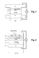
- FIGS. 1 and 2 are, as already said, schematic representations of a radio frequency oscillator according to the prior art.
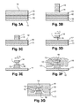
- the Figures 3A to 3G are intended to illustrate the different steps of the process according to the invention.
- step 3A it is assumed that the magnetic stack 10 of the type described in relation to the Figures 1 and 2 has already been deposited on the lower electrode 11. This deposit could be achieved, for example, by sputtering or ion gun.
- a layer 12 of metallic material typically aluminum, designed to oppose the action of the etching that occurs subsequently, and thus temporarily protect magnetic stack 10 during said etching step.
- This "stop" layer 12 is typically made of aluminum by sputtering or ion gun and has a thickness of between 5 and 20 nanometers, for example 10 nanometers.
- a metal layer 13 is deposited , intended to constitute the injector of the nanocontact of the oscillator, that is to say through which will flow the polarized spin current.
- This layer is also carried out for example by sputtering or ion gun.
- the metal used is typically made of tantalum, molybdenum, tungsten or titanium.
- the thickness of this layer is between 50 and 200 nanometers.
- a localized hard mask 14 intended to serve as a mask during the etching of the underlying layers.
- a continuous layer 14 for example chromium or ruthenium or aluminum, which is then etched. It is thus possible, for example, to deposit on the layer 14 a resin 15 which is located vertically above what will serve as a base for the injector by subjecting it to a photolithography step under deep ultraviolet rays or electron beams. . Resin pads are thus obtained, the typical diameter of which is between 100 and 300 nanometers.
- a first etching of the layer 13 constituting the injector is then carried out through the hard mask 14 to give this metal layer 13 its final dimensions.
- reactive ion etching can first be carried out (RIE) of the constituent chromium of the hard mask by chlorine chemistry (for example under Cl 2 or HBr / Cl 2 ), reducing the thickness of this layer 14. Then, we proceed ( figure 3C ) to an RIE etching of the metal layer 13 by fluorinated chemistry SF 6 or CHF 3 or CF 4 with selective stop on the stop layer 12 acting as etch stop layer.
- etching time can typically be increased by 20 to 50% with respect to the time required to reach the barrier layer 12.
- a second etching is performed, for example IBE (" Ion Beam Etching "), through the hard mask 14, in order to suppress, on the one hand, the etching stop layer 12 located outside the zone located in line with the hard mask 14, and secondly, the magnetic stack 10 located outside this same zone.
- IBE etching can be done for example under Argon or Xenon gas, with an angle of incidence of between 5 and 50 degrees.
- This encapsulation is performed by means of a dielectric material, silica or alumina type.
- This encapsulation can be performed by PVD ( Physical Vapor Deposition ) deposition.
- the ALD deposit has the advantage of being very conforming, which allows to marry perfectly the relief of the structure obtained at the figure 3E and in particular the overhang under the mask 14 at the level of the injector 13. This deposit is then completed by a deposit by sputtering or ion gun, faster. We then come to the set illustrated on the figure 3F .
- the nanoplot must be electrically conductive in order to ensure contact between the upper electrode 18 and the injector 13.
- the nanoplot 14 is removed during this step, a wider choice of material is then possible for the hard mask 14, including insulating materials such as SiO 2 or Al 2 O 3 .
- nanoscreens of reduced dimensions typically less than 100 nanometers, or even 50 nanometers, and suitable for optimizing the operating conditions of the radio frequency oscillator resulting therefrom .
Landscapes
- Engineering & Computer Science (AREA)
- Manufacturing & Machinery (AREA)
- Hall/Mr Elements (AREA)
- Chemical Vapour Deposition (AREA)
- Drying Of Semiconductors (AREA)
Applications Claiming Priority (1)
| Application Number | Priority Date | Filing Date | Title |
|---|---|---|---|
| FR0850906A FR2927469B1 (fr) | 2008-02-13 | 2008-02-13 | Procede pour realiser un nanocontact d'une vanne de spin entrant dans la constitution d'un oscillateur radio freqence. |
Publications (2)
| Publication Number | Publication Date |
|---|---|
| EP2091092A1 true EP2091092A1 (de) | 2009-08-19 |
| EP2091092B1 EP2091092B1 (de) | 2010-05-12 |
Family
ID=39712320
Family Applications (1)
| Application Number | Title | Priority Date | Filing Date |
|---|---|---|---|
| EP09305066A Active EP2091092B1 (de) | 2008-02-13 | 2009-01-26 | Verfahren zur Erzeugung eines Nanokontakts in einem Spinventil zur Verwendung bei der Herstellung eines Radiofrequenzoszillators |
Country Status (6)
| Country | Link |
|---|---|
| US (1) | US20090200264A1 (de) |
| EP (1) | EP2091092B1 (de) |
| JP (1) | JP2009194906A (de) |
| AT (1) | ATE467912T1 (de) |
| DE (1) | DE602009000022D1 (de) |
| FR (1) | FR2927469B1 (de) |
Families Citing this family (8)
| Publication number | Priority date | Publication date | Assignee | Title |
|---|---|---|---|---|
| US8233248B1 (en) | 2009-09-16 | 2012-07-31 | Western Digital (Fremont), Llc | Method and system for providing a magnetic recording transducer using a line hard mask |
| KR101080813B1 (ko) | 2009-10-01 | 2011-11-07 | 한국과학기술연구원 | 저전력, 광대역, 고분해력을 갖춘 스핀 디지털 제어 발진기 |
| EP2581940A4 (de) * | 2010-06-10 | 2015-12-09 | Canon Anelva Corp | Oszillationselement und verfahren zur herstellung des oszillationselements |
| EP2410589B1 (de) * | 2010-07-23 | 2013-10-09 | Grützediek, Ursula | Verfahren zur Herstellung eines TMR-Bauelements |
| JP5135419B2 (ja) | 2010-12-03 | 2013-02-06 | 株式会社東芝 | スピントルク発振子、その製造方法、磁気記録ヘッド、磁気ヘッドアセンブリ、磁気記録装置 |
| JP5321851B2 (ja) | 2011-03-25 | 2013-10-23 | 株式会社東芝 | 磁気発振素子及びスピン波装置 |
| US8871102B2 (en) * | 2011-05-25 | 2014-10-28 | Western Digital (Fremont), Llc | Method and system for fabricating a narrow line structure in a magnetic recording head |
| US9034564B1 (en) | 2013-07-26 | 2015-05-19 | Western Digital (Fremont), Llc | Reader fabrication method employing developable bottom anti-reflective coating |
Citations (1)
| Publication number | Priority date | Publication date | Assignee | Title |
|---|---|---|---|---|
| US5695864A (en) | 1995-09-28 | 1997-12-09 | International Business Machines Corporation | Electronic device using magnetic components |
Family Cites Families (9)
| Publication number | Priority date | Publication date | Assignee | Title |
|---|---|---|---|---|
| JPS581878A (ja) * | 1981-06-26 | 1983-01-07 | Fujitsu Ltd | 磁気バブルメモリ素子の製造方法 |
| US6634087B2 (en) * | 2000-12-26 | 2003-10-21 | Headway Technologies, Inc. | Spin valve head having lead overlay |
| US7085100B2 (en) * | 2002-03-19 | 2006-08-01 | Hitachi Global Storage Technologies Netherlands B.V. | Magnetic head having a bilayer pole tip |
| JP3673796B2 (ja) * | 2003-01-14 | 2005-07-20 | Tdk株式会社 | 磁気抵抗効果素子の製造方法、磁気ヘッド、ヘッドサスペンションアセンブリ及び磁気ディスク装置 |
| US6933155B2 (en) * | 2003-05-21 | 2005-08-23 | Grandis, Inc. | Methods for providing a sub .15 micron magnetic memory structure |
| US7280324B2 (en) * | 2004-02-17 | 2007-10-09 | Hitachi Global Storage Technologies Netherlands B.V. | Magnetoresistive sensor having improved antiparallel tab free layer biasing |
| US7770282B2 (en) * | 2005-09-01 | 2010-08-10 | Hitachi Global Storage Technologies Netherlands B.V. | Method of making a magnetic sensing device having an insulator structure |
| US7639456B2 (en) * | 2005-10-06 | 2009-12-29 | Hitachi Global Storage Technologies Netherlands B.V. | Double mill process for patterning current perpendicular to plane (CPP) magnetoresistive devices to minimize barrier shorting and barrier damage |
| US7791844B2 (en) * | 2005-12-14 | 2010-09-07 | Hitachi Global Storage Technologies Netherlands B.V. | Magnetoresistive sensor having a magnetically stable free layer with a positive magnetostriction |
-
2008
- 2008-02-13 FR FR0850906A patent/FR2927469B1/fr not_active Expired - Fee Related
-
2009
- 2009-01-20 US US12/356,237 patent/US20090200264A1/en not_active Abandoned
- 2009-01-26 JP JP2009014714A patent/JP2009194906A/ja active Pending
- 2009-01-26 AT AT09305066T patent/ATE467912T1/de not_active IP Right Cessation
- 2009-01-26 DE DE602009000022T patent/DE602009000022D1/de active Active
- 2009-01-26 EP EP09305066A patent/EP2091092B1/de active Active
Patent Citations (1)
| Publication number | Priority date | Publication date | Assignee | Title |
|---|---|---|---|---|
| US5695864A (en) | 1995-09-28 | 1997-12-09 | International Business Machines Corporation | Electronic device using magnetic components |
Non-Patent Citations (4)
| Title |
|---|
| KISELEV S I ET AL: "Microwave oscillations of a nanomagnet driven by a spin-polarized current", NATURE, NATURE PUBLISHING GROUP, LONDON, UK, vol. 425, 25 September 2003 (2003-09-25), pages 380 - 383, XP002329287, ISSN: 0028-0836 * |
| MANCOFF F B ET AL: "Phase-locking in double-point-contact spin-transfer devices", NATURE NATURE PUBLISHING GROUP UK, vol. 437, no. 7057, 15 September 2005 (2005-09-15), pages 393 - 395, XP002497339, ISSN: 0028-0836 * |
| OZATAY O ET AL: "Spin transfer by nonuniform current injection into a nanomagnet", APPLIED PHYSICS LETTERS, AIP, AMERICAN INSTITUTE OF PHYSICS, MELVILLE, NY, vol. 88, no. 20, 18 May 2006 (2006-05-18), pages 202502 - 202502, XP012081730, ISSN: 0003-6951 * |
| RIPPARD W H ET AL: "Current-driven microwave dynamics in magnetic point contacts as a function of applied field angle", PHYSICAL REVIEW B (CONDENSED MATTER AND MATERIALS PHYSICS) APS THROUGH AIP USA, vol. 70, no. 10, 1 September 2004 (2004-09-01), pages 100406 - 1, XP002497340, ISSN: 0163-1829 * |
Also Published As
| Publication number | Publication date |
|---|---|
| US20090200264A1 (en) | 2009-08-13 |
| EP2091092B1 (de) | 2010-05-12 |
| DE602009000022D1 (de) | 2010-06-24 |
| JP2009194906A (ja) | 2009-08-27 |
| ATE467912T1 (de) | 2010-05-15 |
| FR2927469A1 (fr) | 2009-08-14 |
| FR2927469B1 (fr) | 2010-04-16 |
Similar Documents
| Publication | Publication Date | Title |
|---|---|---|
| EP2091092B1 (de) | Verfahren zur Erzeugung eines Nanokontakts in einem Spinventil zur Verwendung bei der Herstellung eines Radiofrequenzoszillators | |
| EP2417646B1 (de) | Spin-valve- oder tunnel-junction-hochfrequenzoszillator, prozess zum einstellen der frequenz eines solchen oszillators und aus mehreren solchen oszillatoren bestehendes netzwerk | |
| CN109979961B (zh) | 磁阻式随机存取存储器结构及其制造方法 | |
| US10069064B1 (en) | Memory structure having a magnetic tunnel junction (MTJ) self-aligned to a T-shaped bottom electrode, and method of manufacturing the same | |
| US8975089B1 (en) | Method for forming MTJ memory element | |
| US8652856B2 (en) | Method for use in making electronic devices having thin-film magnetic components | |
| US9601688B2 (en) | Method of manufacturing magnetoresistive element and method of processing magnetoresistive film | |
| US10236439B1 (en) | Switching and stability control for perpendicular magnetic tunnel junction device | |
| TW201715762A (zh) | 積體電路及其製造方法 | |
| WO2007010137A1 (fr) | Dispositif radiofrequence avec element magnetique procede de fabrication d'un tel element magnetique | |
| FR2892871A1 (fr) | Oscillateur radio frequence a courant elelctrique polarise en spin | |
| US12075707B2 (en) | Semiconductor structure and method for forming the same | |
| US20190207088A1 (en) | Perpendicular magnetic tunnel junction device with precessional spin current layer having a modulated moment density | |
| FR2939256A1 (fr) | Oscillateur radiofrequence a vanne de spin ou a jonction tunnel | |
| WO2002050886A1 (fr) | Procede de fabrication d'un ilot de matiere confine entre des electrodes, et applications aux transistors | |
| US12048250B2 (en) | Method of fabricating magneto-resistive random access memory (MRAM) | |
| EP2517352B1 (de) | Magnetoresistiver hf-oszillator | |
| WO2011154477A1 (fr) | Oscillateur a transfert de spin | |
| EP2107623B1 (de) | Magnetvorrichtung, die einen magnetoresistiven Stapel und mindestens einen Nanokontakt umfasst | |
| US10141499B1 (en) | Perpendicular magnetic tunnel junction device with offset precessional spin current layer | |
| US12356867B2 (en) | Semiconductor structure and method of manufacture | |
| CN108376690A (zh) | 一种用于制造高密度mram的自对准互联方法 | |
| CN108735893B (zh) | 一种磁性随机存储器底电极接触及其形成方法 | |
| Moneck | Development of novel prototype scalable magnetoresistive random access memory | |
| CN109994476B (zh) | 一种制备磁性随机存储器阵列单元的方法 |
Legal Events
| Date | Code | Title | Description |
|---|---|---|---|
| PUAI | Public reference made under article 153(3) epc to a published international application that has entered the european phase |
Free format text: ORIGINAL CODE: 0009012 |
|
| AK | Designated contracting states |
Kind code of ref document: A1 Designated state(s): AT BE BG CH CY CZ DE DK EE ES FI FR GB GR HR HU IE IS IT LI LT LU LV MC MK MT NL NO PL PT RO SE SI SK TR |
|
| AX | Request for extension of the european patent |
Extension state: AL BA RS |
|
| 17P | Request for examination filed |
Effective date: 20090724 |
|
| 17Q | First examination report despatched |
Effective date: 20090924 |
|
| RTI1 | Title (correction) |
Free format text: METHOD OF ESTABLISHING A NANOCONTACT OF AN IN-SPIN VALVE TO BE USED IN THE MANUFACTURE OF A RADIOFREQUENCY OSCILLATOR |
|
| GRAP | Despatch of communication of intention to grant a patent |
Free format text: ORIGINAL CODE: EPIDOSNIGR1 |
|
| GRAS | Grant fee paid |
Free format text: ORIGINAL CODE: EPIDOSNIGR3 |
|
| GRAA | (expected) grant |
Free format text: ORIGINAL CODE: 0009210 |
|
| AKX | Designation fees paid |
Designated state(s): AT BE BG CH CY CZ DE DK EE ES FI FR GB GR HR HU IE IS IT LI LT LU LV MC MK MT NL NO PL PT RO SE SI SK TR |
|
| RAP1 | Party data changed (applicant data changed or rights of an application transferred) |
Owner name: COMMISSARIAT A L'ENERGIE ATOMIQUE ET AUX ENERGIES |
|
| AK | Designated contracting states |
Kind code of ref document: B1 Designated state(s): AT BE BG CH CY CZ DE DK EE ES FI FR GB GR HR HU IE IS IT LI LT LU LV MC MK MT NL NO PL PT RO SE SI SK TR |
|
| REG | Reference to a national code |
Ref country code: GB Ref legal event code: FG4D Free format text: NOT ENGLISH |
|
| REG | Reference to a national code |
Ref country code: CH Ref legal event code: EP |
|
| REG | Reference to a national code |
Ref country code: IE Ref legal event code: FG4D Free format text: LANGUAGE OF EP DOCUMENT: FRENCH |
|
| REF | Corresponds to: |
Ref document number: 602009000022 Country of ref document: DE Date of ref document: 20100624 Kind code of ref document: P |
|
| REG | Reference to a national code |
Ref country code: NL Ref legal event code: VDEP Effective date: 20100512 |
|
| LTIE | Lt: invalidation of european patent or patent extension |
Effective date: 20100512 |
|
| PG25 | Lapsed in a contracting state [announced via postgrant information from national office to epo] |
Ref country code: ES Free format text: LAPSE BECAUSE OF FAILURE TO SUBMIT A TRANSLATION OF THE DESCRIPTION OR TO PAY THE FEE WITHIN THE PRESCRIBED TIME-LIMIT Effective date: 20100823 Ref country code: LT Free format text: LAPSE BECAUSE OF FAILURE TO SUBMIT A TRANSLATION OF THE DESCRIPTION OR TO PAY THE FEE WITHIN THE PRESCRIBED TIME-LIMIT Effective date: 20100512 Ref country code: NL Free format text: LAPSE BECAUSE OF FAILURE TO SUBMIT A TRANSLATION OF THE DESCRIPTION OR TO PAY THE FEE WITHIN THE PRESCRIBED TIME-LIMIT Effective date: 20100512 Ref country code: NO Free format text: LAPSE BECAUSE OF FAILURE TO SUBMIT A TRANSLATION OF THE DESCRIPTION OR TO PAY THE FEE WITHIN THE PRESCRIBED TIME-LIMIT Effective date: 20100812 Ref country code: SE Free format text: LAPSE BECAUSE OF FAILURE TO SUBMIT A TRANSLATION OF THE DESCRIPTION OR TO PAY THE FEE WITHIN THE PRESCRIBED TIME-LIMIT Effective date: 20100512 |
|
| PG25 | Lapsed in a contracting state [announced via postgrant information from national office to epo] |
Ref country code: AT Free format text: LAPSE BECAUSE OF FAILURE TO SUBMIT A TRANSLATION OF THE DESCRIPTION OR TO PAY THE FEE WITHIN THE PRESCRIBED TIME-LIMIT Effective date: 20100512 Ref country code: FI Free format text: LAPSE BECAUSE OF FAILURE TO SUBMIT A TRANSLATION OF THE DESCRIPTION OR TO PAY THE FEE WITHIN THE PRESCRIBED TIME-LIMIT Effective date: 20100512 Ref country code: HR Free format text: LAPSE BECAUSE OF FAILURE TO SUBMIT A TRANSLATION OF THE DESCRIPTION OR TO PAY THE FEE WITHIN THE PRESCRIBED TIME-LIMIT Effective date: 20100512 Ref country code: IS Free format text: LAPSE BECAUSE OF FAILURE TO SUBMIT A TRANSLATION OF THE DESCRIPTION OR TO PAY THE FEE WITHIN THE PRESCRIBED TIME-LIMIT Effective date: 20100912 Ref country code: LV Free format text: LAPSE BECAUSE OF FAILURE TO SUBMIT A TRANSLATION OF THE DESCRIPTION OR TO PAY THE FEE WITHIN THE PRESCRIBED TIME-LIMIT Effective date: 20100512 Ref country code: SI Free format text: LAPSE BECAUSE OF FAILURE TO SUBMIT A TRANSLATION OF THE DESCRIPTION OR TO PAY THE FEE WITHIN THE PRESCRIBED TIME-LIMIT Effective date: 20100512 |
|
| REG | Reference to a national code |
Ref country code: IE Ref legal event code: FD4D |
|
| PG25 | Lapsed in a contracting state [announced via postgrant information from national office to epo] |
Ref country code: CY Free format text: LAPSE BECAUSE OF FAILURE TO SUBMIT A TRANSLATION OF THE DESCRIPTION OR TO PAY THE FEE WITHIN THE PRESCRIBED TIME-LIMIT Effective date: 20100616 Ref country code: PL Free format text: LAPSE BECAUSE OF FAILURE TO SUBMIT A TRANSLATION OF THE DESCRIPTION OR TO PAY THE FEE WITHIN THE PRESCRIBED TIME-LIMIT Effective date: 20100512 |
|
| PG25 | Lapsed in a contracting state [announced via postgrant information from national office to epo] |
Ref country code: IE Free format text: LAPSE BECAUSE OF FAILURE TO SUBMIT A TRANSLATION OF THE DESCRIPTION OR TO PAY THE FEE WITHIN THE PRESCRIBED TIME-LIMIT Effective date: 20100512 Ref country code: DK Free format text: LAPSE BECAUSE OF FAILURE TO SUBMIT A TRANSLATION OF THE DESCRIPTION OR TO PAY THE FEE WITHIN THE PRESCRIBED TIME-LIMIT Effective date: 20100512 Ref country code: EE Free format text: LAPSE BECAUSE OF FAILURE TO SUBMIT A TRANSLATION OF THE DESCRIPTION OR TO PAY THE FEE WITHIN THE PRESCRIBED TIME-LIMIT Effective date: 20100512 |
|
| PG25 | Lapsed in a contracting state [announced via postgrant information from national office to epo] |
Ref country code: SK Free format text: LAPSE BECAUSE OF FAILURE TO SUBMIT A TRANSLATION OF THE DESCRIPTION OR TO PAY THE FEE WITHIN THE PRESCRIBED TIME-LIMIT Effective date: 20100512 Ref country code: RO Free format text: LAPSE BECAUSE OF FAILURE TO SUBMIT A TRANSLATION OF THE DESCRIPTION OR TO PAY THE FEE WITHIN THE PRESCRIBED TIME-LIMIT Effective date: 20100512 Ref country code: CZ Free format text: LAPSE BECAUSE OF FAILURE TO SUBMIT A TRANSLATION OF THE DESCRIPTION OR TO PAY THE FEE WITHIN THE PRESCRIBED TIME-LIMIT Effective date: 20100512 |
|
| PLBE | No opposition filed within time limit |
Free format text: ORIGINAL CODE: 0009261 |
|
| STAA | Information on the status of an ep patent application or granted ep patent |
Free format text: STATUS: NO OPPOSITION FILED WITHIN TIME LIMIT |
|
| 26N | No opposition filed |
Effective date: 20110215 |
|
| PG25 | Lapsed in a contracting state [announced via postgrant information from national office to epo] |
Ref country code: GR Free format text: LAPSE BECAUSE OF FAILURE TO SUBMIT A TRANSLATION OF THE DESCRIPTION OR TO PAY THE FEE WITHIN THE PRESCRIBED TIME-LIMIT Effective date: 20100813 |
|
| PGFP | Annual fee paid to national office [announced via postgrant information from national office to epo] |
Ref country code: FR Payment date: 20110202 Year of fee payment: 3 |
|
| REG | Reference to a national code |
Ref country code: DE Ref legal event code: R097 Ref document number: 602009000022 Country of ref document: DE Effective date: 20110214 |
|
| BERE | Be: lapsed |
Owner name: COMMISSARIAT A L'ENERGIE ATOMIQUE ET AUX ENERGIES Effective date: 20110131 |
|
| PG25 | Lapsed in a contracting state [announced via postgrant information from national office to epo] |
Ref country code: MC Free format text: LAPSE BECAUSE OF NON-PAYMENT OF DUE FEES Effective date: 20110131 |
|
| PG25 | Lapsed in a contracting state [announced via postgrant information from national office to epo] |
Ref country code: BE Free format text: LAPSE BECAUSE OF NON-PAYMENT OF DUE FEES Effective date: 20110131 |
|
| PG25 | Lapsed in a contracting state [announced via postgrant information from national office to epo] |
Ref country code: MT Free format text: LAPSE BECAUSE OF FAILURE TO SUBMIT A TRANSLATION OF THE DESCRIPTION OR TO PAY THE FEE WITHIN THE PRESCRIBED TIME-LIMIT Effective date: 20100512 |
|
| PGFP | Annual fee paid to national office [announced via postgrant information from national office to epo] |
Ref country code: DE Payment date: 20120118 Year of fee payment: 4 |
|
| PGFP | Annual fee paid to national office [announced via postgrant information from national office to epo] |
Ref country code: IT Payment date: 20120131 Year of fee payment: 4 |
|
| REG | Reference to a national code |
Ref country code: FR Ref legal event code: ST Effective date: 20120928 |
|
| PG25 | Lapsed in a contracting state [announced via postgrant information from national office to epo] |
Ref country code: FR Free format text: LAPSE BECAUSE OF NON-PAYMENT OF DUE FEES Effective date: 20120131 |
|
| PG25 | Lapsed in a contracting state [announced via postgrant information from national office to epo] |
Ref country code: LU Free format text: LAPSE BECAUSE OF NON-PAYMENT OF DUE FEES Effective date: 20110126 |
|
| PG25 | Lapsed in a contracting state [announced via postgrant information from national office to epo] |
Ref country code: PT Free format text: LAPSE BECAUSE OF NON-PAYMENT OF DUE FEES Effective date: 20100512 |
|
| REG | Reference to a national code |
Ref country code: CH Ref legal event code: PL |
|
| GBPC | Gb: european patent ceased through non-payment of renewal fee |
Effective date: 20130126 |
|
| PG25 | Lapsed in a contracting state [announced via postgrant information from national office to epo] |
Ref country code: TR Free format text: LAPSE BECAUSE OF FAILURE TO SUBMIT A TRANSLATION OF THE DESCRIPTION OR TO PAY THE FEE WITHIN THE PRESCRIBED TIME-LIMIT Effective date: 20100512 Ref country code: BG Free format text: LAPSE BECAUSE OF FAILURE TO SUBMIT A TRANSLATION OF THE DESCRIPTION OR TO PAY THE FEE WITHIN THE PRESCRIBED TIME-LIMIT Effective date: 20100812 |
|
| PG25 | Lapsed in a contracting state [announced via postgrant information from national office to epo] |
Ref country code: DE Free format text: LAPSE BECAUSE OF NON-PAYMENT OF DUE FEES Effective date: 20130801 Ref country code: LI Free format text: LAPSE BECAUSE OF NON-PAYMENT OF DUE FEES Effective date: 20130131 Ref country code: CH Free format text: LAPSE BECAUSE OF NON-PAYMENT OF DUE FEES Effective date: 20130131 Ref country code: HU Free format text: LAPSE BECAUSE OF FAILURE TO SUBMIT A TRANSLATION OF THE DESCRIPTION OR TO PAY THE FEE WITHIN THE PRESCRIBED TIME-LIMIT Effective date: 20100512 |
|
| REG | Reference to a national code |
Ref country code: DE Ref legal event code: R119 Ref document number: 602009000022 Country of ref document: DE Effective date: 20130801 |
|
| PG25 | Lapsed in a contracting state [announced via postgrant information from national office to epo] |
Ref country code: GB Free format text: LAPSE BECAUSE OF NON-PAYMENT OF DUE FEES Effective date: 20130126 |
|
| PG25 | Lapsed in a contracting state [announced via postgrant information from national office to epo] |
Ref country code: IT Free format text: LAPSE BECAUSE OF NON-PAYMENT OF DUE FEES Effective date: 20130126 |