EP2091096A1 - Dispositif électronique encapsulé et procédé de fabrication - Google Patents
Dispositif électronique encapsulé et procédé de fabrication Download PDFInfo
- Publication number
- EP2091096A1 EP2091096A1 EP08151524A EP08151524A EP2091096A1 EP 2091096 A1 EP2091096 A1 EP 2091096A1 EP 08151524 A EP08151524 A EP 08151524A EP 08151524 A EP08151524 A EP 08151524A EP 2091096 A1 EP2091096 A1 EP 2091096A1
- Authority
- EP
- European Patent Office
- Prior art keywords
- electronic device
- layer
- inorganic
- barrier structure
- organic layer
- Prior art date
- Legal status (The legal status is an assumption and is not a legal conclusion. Google has not performed a legal analysis and makes no representation as to the accuracy of the status listed.)
- Withdrawn
Links
Images


Classifications
-
- H—ELECTRICITY
- H10—SEMICONDUCTOR DEVICES; ELECTRIC SOLID-STATE DEVICES NOT OTHERWISE PROVIDED FOR
- H10K—ORGANIC ELECTRIC SOLID-STATE DEVICES
- H10K50/00—Organic light-emitting devices
- H10K50/80—Constructional details
- H10K50/84—Passivation; Containers; Encapsulations
- H10K50/844—Encapsulations
- H10K50/8445—Encapsulations multilayered coatings having a repetitive structure, e.g. having multiple organic-inorganic bilayers
-
- B—PERFORMING OPERATIONS; TRANSPORTING
- B82—NANOTECHNOLOGY
- B82Y—SPECIFIC USES OR APPLICATIONS OF NANOSTRUCTURES; MEASUREMENT OR ANALYSIS OF NANOSTRUCTURES; MANUFACTURE OR TREATMENT OF NANOSTRUCTURES
- B82Y30/00—Nanotechnology for materials or surface science, e.g. nanocomposites
-
- B—PERFORMING OPERATIONS; TRANSPORTING
- B82—NANOTECHNOLOGY
- B82Y—SPECIFIC USES OR APPLICATIONS OF NANOSTRUCTURES; MEASUREMENT OR ANALYSIS OF NANOSTRUCTURES; MANUFACTURE OR TREATMENT OF NANOSTRUCTURES
- B82Y20/00—Nanooptics, e.g. quantum optics or photonic crystals
-
- H—ELECTRICITY
- H05—ELECTRIC TECHNIQUES NOT OTHERWISE PROVIDED FOR
- H05B—ELECTRIC HEATING; ELECTRIC LIGHT SOURCES NOT OTHERWISE PROVIDED FOR; CIRCUIT ARRANGEMENTS FOR ELECTRIC LIGHT SOURCES, IN GENERAL
- H05B33/00—Electroluminescent light sources
- H05B33/02—Details
- H05B33/04—Sealing arrangements, e.g. against humidity
-
- H—ELECTRICITY
- H10—SEMICONDUCTOR DEVICES; ELECTRIC SOLID-STATE DEVICES NOT OTHERWISE PROVIDED FOR
- H10K—ORGANIC ELECTRIC SOLID-STATE DEVICES
- H10K50/00—Organic light-emitting devices
- H10K50/80—Constructional details
- H10K50/805—Electrodes
-
- H—ELECTRICITY
- H10—SEMICONDUCTOR DEVICES; ELECTRIC SOLID-STATE DEVICES NOT OTHERWISE PROVIDED FOR
- H10K—ORGANIC ELECTRIC SOLID-STATE DEVICES
- H10K50/00—Organic light-emitting devices
- H10K50/80—Constructional details
- H10K50/85—Arrangements for extracting light from the devices
- H10K50/854—Arrangements for extracting light from the devices comprising scattering means
-
- H—ELECTRICITY
- H10—SEMICONDUCTOR DEVICES; ELECTRIC SOLID-STATE DEVICES NOT OTHERWISE PROVIDED FOR
- H10K—ORGANIC ELECTRIC SOLID-STATE DEVICES
- H10K50/00—Organic light-emitting devices
- H10K50/80—Constructional details
- H10K50/85—Arrangements for extracting light from the devices
- H10K50/858—Arrangements for extracting light from the devices comprising refractive means, e.g. lenses
-
- H—ELECTRICITY
- H10—SEMICONDUCTOR DEVICES; ELECTRIC SOLID-STATE DEVICES NOT OTHERWISE PROVIDED FOR
- H10K—ORGANIC ELECTRIC SOLID-STATE DEVICES
- H10K71/00—Manufacture or treatment specially adapted for the organic devices covered by this subclass
- H10K71/80—Manufacture or treatment specially adapted for the organic devices covered by this subclass using temporary substrates
-
- H—ELECTRICITY
- H10—SEMICONDUCTOR DEVICES; ELECTRIC SOLID-STATE DEVICES NOT OTHERWISE PROVIDED FOR
- H10K—ORGANIC ELECTRIC SOLID-STATE DEVICES
- H10K2102/00—Constructional details relating to the organic devices covered by this subclass
- H10K2102/301—Details of OLEDs
- H10K2102/331—Nanoparticles used in non-emissive layers, e.g. in packaging layer
Definitions
- the present invention relates to an encapsulated electronic device.
- the present invention further relates to a method of manufacturing an encapsulated electronic device.
- a new generation of thin film based devices such as organic light emitting diodes (OLED) for lighting and displays, thin film batteries, thin film organic solar cells, electrochromic foils, electrophoretic displays, etc., have the potential to become a next revolution in electronic systems. These thin film devices have to be protected from contamination by moisture. For that purpose, the last decade several thin film barrier coatings have been developed, often based on a stack of organic and inorganic layers.
- the moisture protected thin film based devices described therein comprises a foundation having a top of a first polymer layer, a first ceramic layer on the first polymer layer, and a second polymer layer on the first ceramic layer.
- An organic light emitting device is constructed on the second polymer layer of the top of the foundation.
- a cover is deposited on the organic light emitting device.
- the cover comprises subsequently a third polymer layer with a second ceramic layer thereon and a fourth polymer layer on said second ceramic layer.
- the foundation and the cover encapsulate the organic light emitting device as a flexible environmental barrier.
- an encapsulated electronic device comprising:
- the at least one inorganic layer of the first barrier structure and the at least one inorganic layer of the second barrier structure contact each outside an area occupied by the electronic device. In this way a lateral penetration of moisture toward the electronic device is counteracted.
- the said inorganic layer contact each other over a part of a circumference around the electronic device, preferably the said inorganic layers substantially contact each other at a full circumference around the electronic device.
- the at least one inorganic layer of the first barrier structure and the at least one inorganic layer of the second barrier structure cooperate to encapsulate the electronic device laterally. Nevertheless the contact between the said inorganic layers may be interrupted by electrical conductors coupled to the electronic device.
- the inorganic layers are separated by organic layers. Accordingly the inorganic layers cannot prevent that moisture in the environment of the device penetrates laterally towards the device.
- the first barrier structure comprises a first inorganic layer, a first organic layer forming the at least one organic layer and a second inorganic layer forming the at least one inorganic layer, the first organic layer being arranged between the first and the second inorganic layer.
- an organic layer has micro-holes, which could form a path for moisture.
- the probability is small that the micro-holes in these layers are positioned opposite to each other. Accordingly, the probability of a leak of moisture is substantially reduced.
- the second barrier structure comprises a third inorganic layer forming the at least one inorganic layer, a second organic layer forming the at least one organic layer and a fourth inorganic layer, the second organic layer being arranged between the third and the fourth inorganic layer.
- At least one organic layer comprises a moisture getter.
- An embodiment of the encapsulated electronic device is characterized in that the first barrier structure and the second barrier structure have a substantially equal thickness and configuration.
- the amount of deformation of the electronic device between the barrier structures is as small as possible in case the encapsulated electronic device is bended.
- An embodiment of the encapsulated electronic device is characterized in that the electronic device is an OLED device, and in that a patterned additional organic layer is applied at at least one of the barrier structures at a side remote from the electronic device.
- a patterned additional organic layer improves an output efficiency of visible or non-visible radiation generated by the OLED. Additionally the pattern may be used to control a direction in which radiation emanates from the encapsulated electronic device.
- the encapsulated electronic device may be characterized in that at least one organic layer comprises optically active particles. Also in this way the outcoupling of light may be improved.
- the optically active particles are microlenses. In an other embodiment the optically active particles are scattering particles.
- An encapsulated electronic device according to the invention may be manufactured with an inventive method comprising the steps of
- the substrate facilitates the handling of the thin film based device under construction as it provides stiffness thereto. It is however desirable to remove the substrate at the end, as it is often preferred that the end-product is more flexible. It has, however, been observed that removal of the substrate tended to lead to premature failure of the product and therewith resulted in a decrease of the yield of the manufacturing process.
- the encapsulated electronic device is released from the substrate after its completion and the substrate is made of an inorganic material. It was found by the inventors that this embodiment of the method results in an increased yield, as compared to a method wherein a substrate of an organic material is removed from the encapsulated electronic product.
- a preferred embodiment of the method of manufacturing an encapsulated electronic device is characterized in that the substrate or a release layer thereon is patterned.
- the patterned substrate or the release layer then functions as a template for the first inorganic layer that is applied on the substrate. In this way a patterned additional inorganic layer that improves an output efficiency of the encapsulated electronic device is realized without additional manufacturing steps.
- the inorganic layers may be applied by all kinds of physical vapour deposition methods such as thermal evaporation, e-beam evaporation, sputtering, magnetron sputtering, reactive sputtering, reactive evaporation, etc. and all kinds of chemical vapour deposition methods such as thermal chemical vapour deposition (CVD), photo assisted chemical vapour deposition (PACVD), plasma enhanced chemical vapour deposition (PECVD), etc.
- physical vapour deposition methods such as thermal evaporation, e-beam evaporation, sputtering, magnetron sputtering, reactive sputtering, reactive evaporation, etc.
- chemical vapour deposition methods such as thermal chemical vapour deposition (CVD), photo assisted chemical vapour deposition (PACVD), plasma enhanced chemical vapour deposition (PECVD), etc.
- the organic layers may be applied by all kinds of coatings techniques, such spin coating, slot-die coating, kiss-coating, hot-melt coating, spray coating, etc. and all kinds of printing techniques, such as inkjet printing, gravure printing, flexographic printing, screen printing, rotary screen printing, etc.
- coatings techniques such spin coating, slot-die coating, kiss-coating, hot-melt coating, spray coating, etc.
- printing techniques such as inkjet printing, gravure printing, flexographic printing, screen printing, rotary screen printing, etc.
- embodiments of the invention should not be construed as limited to the particular shapes of regions illustrated herein but are to include deviations in shapes that result, for example, from manufacturing.
- the regions illustrated in the figures are schematic in nature and their shapes are not intended to illustrate the actual shape of a region of a device and are not intended to limit the scope of the invention.
- first, second, third etc. may be used herein to describe various elements, components, regions, layers and/or sections, these elements, components, regions, layers and/or sections should not be limited by these terms. These terms are only used to distinguish one element, component, region, layer or section from another region, layer or section. Thus, a first element, component, region, layer or section discussed below could be termed a second element, component, region, layer or section without departing from the teachings of the present invention.
- spatially relative terms such as “beneath”, “below”, “lower”, “above”, “upper” and the like, may be used herein for ease of description to describe one element or feature's relationship to another element(s) or feature(s) as illustrated in the figures. It will be understood that the spatially relative terms are intended to encompass different orientations of the device in use or operation in addition to the orientation depicted in the figures. For example, if the device in the figures is turned over, elements described as “below” or “beneath” other elements or features would then be oriented “above” the other elements or features. Thus, the exemplary term “below” can encompass both an orientation of above and below. The device may be otherwise oriented (rotated 90 degrees or at other orientations) and the spatially relative descriptors used herein interpreted accordingly.
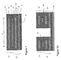
- Figure 1 shows an example of an encapsulated electronic device obtained with a method according to the invention
- the encapsulated electronic device comprises an electronic device 10 that is encapsulated between a first barrier structure 20 and a second barrier structure 30. More in particular the first barrier structure 20 comprises at least one inorganic 24 at least one organic layer 23. Likewise, the second barrier structure 30 comprises at least one inorganic layer 31 and at least one organic layer 32. The at least one inorganic layer 24 of the first barrier structure 20 and the at least one inorganic layer 31 of the second barrier structure 30 contact each other outside an area A occupied by the electronic device 10.
- the organic layer may comprise a moisture getter. Suitable organic materials for this purpose may include, but are not limited to
- Inorganic getter materials are preferably provided as particles in an organic layer.
- CaO or MgO particles are suitable for this purpose.
- the first barrier structure 20 comprises a firs inorganic layer 22, a first organic layer 23 forming the at least one organic layer and a second inorganic layer 24 forming the at least one inorganic layer.
- the first organic layer 23 is arranged between the first and the second inorganic layer 22, 24.
- the second barrier structure 30 comprises a third inorganic layer 31 forming the at least one inorganic layer, a second organic layer 32 forming the at least one organic layer and a fourth inorganic layer 33.
- the second organic layer 32 is arranged between the third and the fourth inorganic layer 31, 33.
- an additional organic layer 21 is applied at at least one of the barrier structures 20 at a side remote from the electronic device 10. Furthermore a release layer 51 is provided with which the stack 10, 20, 30 was released from a substrate.
- the electronic device is for example an organic light emitting diode (OLED) for lighting and displays, a thin film battery, a thin film organic solar cell, an electrochromic foil or an electrophoretic displays.
- OLED organic light emitting diode
- the inorganic layers have a water vapour transmission rate of at most 10 -4 g.m -2 .day -1 .
- the organic layers may be provided from a cross-linked (thermoset) material, an elastomer, a linear polymer, or a branched or hyper-branched polymer system or any combination of the aforementioned, optionally filled with inorganic particles of a size small enough to still guarantee light transmission.
- the material is processed either from solution or as a 100% solids material. Curing or drying may exemplary occur by irradiation of the wet material, pure, or suitably formulated with a photo- or heat-sensitive radical or super-acid initiator, with UV-light, visible light, infrared light or heat, E-beam, g-rays or any combination of the aforementioned.
- the material of the organic layer preferably has a low specific water vapour transmission rate and a high hydrophobicity.
- suitable cross-linking (thermoset) systems are any single one or any combination of aliphatic or aromatic epoxy acrylates, urethane acrylates, polyester acrylates, polyether acrylates, saturated hydrocarbon acrylates, epoxides, epoxide-amine systems, epoxide-carboxylic acid combinations, oxetanes, vinyl ethers, vinyl derivatives, and thiol-ene systems.
- Suitable examples of elastomeric materials are polysiloxanes.
- Suitable branched or linear polymeric systems are any single one or any copolymer or physical combination of polyacrylates, polyesters, polyethers, polypropylenes, polyethylenes, polybutadienes, polynorbornene, cyclic olefin copolymers, polyvinylidenefluoride, polyvinylidenechloride, polyvinylchloride, polytetrafluoroethylene, polychlorotrifluoroethylene, polyhexafluoropropylene.
- the organic layers may have a thickness between 0.1 - 100 ⁇ m, preferably between 5 and 50 ⁇ m.
- the inorganic layer(s) may be any ceramic including but not limited to metal oxide, such as indium oxide (In2O3), tin oxide (SnO2), indium tin oxide (ITO), a metal nitride, such as aluminium nitride (AIN), silicon nitride (SiN), a carbide, such as silicon carbide, a metal oxynitride, e.g. siliconoxynitride, or any other combination such as metal oxy carbides, metal carbonitrides, metal oxycarbonitrides.
- metal oxide such as indium oxide (In2O3), tin oxide (SnO2), indium tin oxide (ITO)
- a metal nitride such as aluminium nitride (AIN), silicon nitride (SiN)
- a carbide such as silicon carbide, a metal oxynitride, e.g. siliconoxynitride, or any other combination such as metal oxy carb
- Suitable materials therefore are for example silicon oxide (SiO2), aluminum oxide (Al2O3), titanium oxide (TiO2), indium oxide (In2O3) tin oxide (SnO2), indium tin oxide (ITO, In203+SnO2), (SiC), silicon oxynitride (SiON) and combinations thereof.
- the inorganic layer(s) are in practice substantially thinner than the organic layers.
- the inorganic layers should have a thickness in the range of 10 to 1000 nm, preferably in the range of 100 to 300 nm.
- the total thickness of the first and the second barrier layer is preferably at least 50 ⁇ m. At a thickness substantially smaller than 50 ⁇ m, e.g. 20 ⁇ m, the resulting encapsulated electronic device tends to damage to quickly. Preferably the total thickness is less than 500 ⁇ m. If the thickness is substantially more, e.g. 1 mm, the flexibility of the product is impaired.
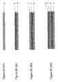
- a substrate 50 is provided.
- the substrate is made of an inorganic material.
- the inorganic material may comprise e.g. a ceramic material, a glass or a metal.
- step 2B a release layer 51 is applied on the substrate.
- the methods described above for applying an organic layer are suitable for this purpose.
- the release layer may comprise a silica organic based polymer such as polydimethylsiloxaan (PDMS), but may alternatively comprise another component that provides for a sufficient adhesion of the workpiece to the substrate 50 during manufacturing, but that allows an easy release of the workpiece once finished.
- PDMS polydimethylsiloxaan
- materials used in the active layers of OLED devices, like PEDOT and LEP turned out to be suitable for this purpose.
- the release layer 51 may stay with the product, or may stay with the substrate 50. If the release layer stays with the substrate it may be reused or removed.
- steps S3 to S5 a first barrier structure 20 is applied at the release layer.
- steps S3 to S5 a first barrier structure 20 is applied at the release layer.
- steps S3 to S5 a first barrier structure 20 is applied at the release layer.
- these steps comprise:
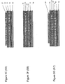
- step S7 an organic thin film electronic device is constructed.
- OLEDs e.g. OLEDs, OFETs, organic solar cells etc.
- steps S8 to S9 a second barrier structure 30 is applied on top of the organic thin film electronic device.
- Step S8 wherein a third inorganic layer 31 is applied
- Step S9 wherein a second organic layer 32 is applied at the third inorganic layer 31, and
- Step S10 wherein a fourth inorganic layer 33 is applied at the first organic layer 32.
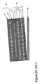
- a subsequent step S11 shown in Figure 2K , the product formed in the previous steps is released from the substrate 50. Therewith an encapsulated electronic device as shown in Figure 1 is obtained. As shown in Figure 1A more devices may be constructed on a single substrate 50.
- the electronic device 10 is electrically connected to external conductors.
- the electrical conductors to the electronic device are provided as an aluminium conductor with an molybdenum coating between subsequent inorganic layers 24, 21 for example.
- the molybdenum coating therein service as an adhesion layer.
- This step of applying the electrical conductors can be applied between step S7 and S8 according to the method described above.
- an electrical connection to outside conductors is provided later, e.g. after step 2K. This is possible by punching respective holes through at least one of the barrier layers towards electrical connectors of the electronic device and filling these holes with a conductive material.
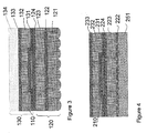
- FIG. 3 shows a preferred embodiment of the encapsulated electronic device according to the invention.
- the encapsulated electronic device i.e. an OLED shown therein comprises a patterned additional organic layer 121 that is applied at at least one of the barrier structures at a side remote from the electronic device.
- the pattern in the additional organic layer forms an array of microlenses that improve light outcoupling of the OLED.
- additional organic layer 121 is a release layer, and the pattern therein was obtained by using a substrate 50 with a complimentary pattern during the manufacturing steps illustrated in Figure 2A-2K .
- the second barrier structure 130 may include an additional organic layer 134. In this way it is achieved that the first and the second barrier structure 120, 130 have a substantially equal thickness.
- Figure 4 shows a second preferred embodiment. Parts therein corresponding to those in Figure 1 have a reference number that is 200 higher.
- the release layer 251 is provided with a patterned surface pointing away from the substrate 50, between step S2 and S3 as illustrated in Figures2B and 2C respectively.
- the first inorganic layer 222 follows this pattern. In this way a pattern of microlenses may be obtained between two organic layers 251, 223.
- the additional organic layer 351 comprises optically active particles 355, here, scattering particles.
- the scattering particles 351 have a relatively high refractive index (higher than 2 for example) with respect to the organic matrix that has low refractive index (1.5-1.6).
- the scattering particles are for example of titania (TiO 2 ) or zirconia (ZrO 2 ) particles.
- the function of the particles 355 is illustrated in Figure 5B .
- Light emerges from the active layers of the OLED with an angular distribution at position "a”.
- the ray impinges upon a particulate scatterer at "b”, and is back scattered to point "c", which is the surface of the active layers of the OLED, for example an indium tin oxide layer (ITO).
- ITO indium tin oxide layer
- the ray is reflected at point "c”, but also attenuated due to the finite reflectivity of the OLED.
- the ray then travels to point “d”, is scattered again, and reaches the top air-glass interface a point "e” with an angle of incidence that exceeds the critical angle and undergoes total internal reflection.
- the ray is reflected back to a scattering particle ("f"), is back-scattered toward the air substrate interface (point “g”). This time the angle of incidence is less than the critical angle and the ray is transmitted across the interface.
- the optically active particles 355 in the additional layer 351 may be microlenses. By selecting a distribution and shape of the optically active particles, the distribution of light emanating from the OLED may be controlled.
- the material to be selected for the micro lenses depends on the position where they are placed in the device. For example on the most outer substrate area they should have a refractive index lower than that of the layer that borders to the layer of micro lenses and close to the refractive index of air. If they are placed in a polymer matrix, e.g. in layer 323, or layer 332, they might have higher refractive index.
- shaped lenses In the case of shaped lenses, they can be either embedded into the organic matrix/or shaped by soft lithography,etc/but they can also be on top and the next inorganic layer will follow them. In this case they might have the same or different refractive index as the organic layer.
- the microlenses primarily widen the escape cone for total internally reflected light incident at the air-substrate boundary.
- the microlenses simply redirect the light without introducing microcavities or other undesirable parasitic optical effects.
- the extraction of light at angles higher than the critical angle of substrate is enhanced.
- the height of the microlenses may range from lum up to 100 um and the planar size is comparable or larger than the maximum wavelength of visible light emitted from the OLEDs and smaller than the OLED area (for example ranging from 1 um up to 50 um).
- the microlens density can vary from 5000 to about 1 000 000 lenses per square millimeter and will depend on their size.
- the shape of the microlenses is processed in such way that they do not introduce angular dependence or anisotropy.
- the microlenses may have a hemispheric shape, but may alternatively have the shape of a polyhedron, such as a trunked pyramid.
Landscapes
- Chemical & Material Sciences (AREA)
- Engineering & Computer Science (AREA)
- Physics & Mathematics (AREA)
- Nanotechnology (AREA)
- Optics & Photonics (AREA)
- Crystallography & Structural Chemistry (AREA)
- Manufacturing & Machinery (AREA)
- Inorganic Chemistry (AREA)
- Biophysics (AREA)
- Composite Materials (AREA)
- Condensed Matter Physics & Semiconductors (AREA)
- General Physics & Mathematics (AREA)
- Materials Engineering (AREA)
- Life Sciences & Earth Sciences (AREA)
- Electroluminescent Light Sources (AREA)
- Structures Or Materials For Encapsulating Or Coating Semiconductor Devices Or Solid State Devices (AREA)
- Hybrid Cells (AREA)
Priority Applications (8)
| Application Number | Priority Date | Filing Date | Title |
|---|---|---|---|
| EP08151524A EP2091096A1 (fr) | 2008-02-15 | 2008-02-15 | Dispositif électronique encapsulé et procédé de fabrication |
| EP09711180.1A EP2255399B1 (fr) | 2008-02-15 | 2009-02-13 | Procédé de fabrication d'un dispositif électronique encapsulé |
| PCT/NL2009/050061 WO2009102201A1 (fr) | 2008-02-15 | 2009-02-13 | Dispositif électronique encapsulé et son procédé de fabrication |
| JP2010546716A JP5723158B2 (ja) | 2008-02-15 | 2009-02-13 | 封入型電子装置および製造方法 |
| CN2009801130279A CN102007616A (zh) | 2008-02-15 | 2009-02-13 | 封装的电子设备及其制备方法 |
| US12/867,748 US20110171764A1 (en) | 2008-02-15 | 2009-02-13 | Encapsulated electronic device and method of manufacturing |
| KR1020107020586A KR20110008163A (ko) | 2008-02-15 | 2009-02-13 | 캡슐화된 전자 장치 및 이의 제조방법 |
| TW098104800A TWI533486B (zh) | 2008-02-15 | 2009-02-16 | 封裝電子元件及其製造方法 |
Applications Claiming Priority (1)
| Application Number | Priority Date | Filing Date | Title |
|---|---|---|---|
| EP08151524A EP2091096A1 (fr) | 2008-02-15 | 2008-02-15 | Dispositif électronique encapsulé et procédé de fabrication |
Publications (1)
| Publication Number | Publication Date |
|---|---|
| EP2091096A1 true EP2091096A1 (fr) | 2009-08-19 |
Family
ID=39591075
Family Applications (2)
| Application Number | Title | Priority Date | Filing Date |
|---|---|---|---|
| EP08151524A Withdrawn EP2091096A1 (fr) | 2008-02-15 | 2008-02-15 | Dispositif électronique encapsulé et procédé de fabrication |
| EP09711180.1A Not-in-force EP2255399B1 (fr) | 2008-02-15 | 2009-02-13 | Procédé de fabrication d'un dispositif électronique encapsulé |
Family Applications After (1)
| Application Number | Title | Priority Date | Filing Date |
|---|---|---|---|
| EP09711180.1A Not-in-force EP2255399B1 (fr) | 2008-02-15 | 2009-02-13 | Procédé de fabrication d'un dispositif électronique encapsulé |
Country Status (7)
| Country | Link |
|---|---|
| US (1) | US20110171764A1 (fr) |
| EP (2) | EP2091096A1 (fr) |
| JP (1) | JP5723158B2 (fr) |
| KR (1) | KR20110008163A (fr) |
| CN (1) | CN102007616A (fr) |
| TW (1) | TWI533486B (fr) |
| WO (1) | WO2009102201A1 (fr) |
Cited By (11)
| Publication number | Priority date | Publication date | Assignee | Title |
|---|---|---|---|---|
| WO2012009729A1 (fr) * | 2010-07-16 | 2012-01-19 | Sumitomo Chemical Co., Ltd. | Additifs organiques pour durées de vie allongées de dispositifs électroniques organiques et pouvant être traités par une solution |
| CN102509719A (zh) * | 2011-09-21 | 2012-06-20 | 友达光电股份有限公司 | 可挠式显示器的制作方法以及可挠式显示器 |
| EP2564444A1 (fr) * | 2010-04-29 | 2013-03-06 | Nederlandse Organisatie voor toegepast -natuurwetenschappelijk onderzoek TNO | Dispositif électroluminescent et son procédé de fabrication |
| CN103430345A (zh) * | 2010-10-25 | 2013-12-04 | 荷兰应用自然科学研究组织Tno | 多层保护层、有机光电器件及其制造方法 |
| KR20140007340A (ko) * | 2010-10-25 | 2014-01-17 | 네덜란제 오르가니자티에 포오르 토에게파스트-나투우르베텐샤펠리즈크 온데르조에크 테엔오 | 광전자 소자 및 광전자 소자의 제조 방법 |
| EP2806473A1 (fr) * | 2013-05-24 | 2014-11-26 | Samsung Display Co., Ltd. | Appareil d'affichage électroluminescent organique comprenant un substrat souple |
| EP2804231A3 (fr) * | 2013-05-16 | 2015-05-06 | Samsung Display Co., Ltd. | Affichage à diode électroluminescente organique, dispositif électronique comprenant celui-ci et procédé de fabrication dudit dispositif d'affichage |
| US9178178B2 (en) | 2013-05-16 | 2015-11-03 | Samsung Display Co., Ltd. | Organic light-emitting diode display having improved adhesion and damage resistance characteristics, an electronic device including the same, and method of manufacturing the organic light-emitting diode display |
| EP2765623A3 (fr) * | 2013-02-07 | 2016-09-28 | Samsung Display Co., Ltd. | Dispositif d'affichage flexible et procédé de fabrication de dispositif d'affichage flexible |
| EP3183725A4 (fr) * | 2014-08-24 | 2018-04-11 | Royole Corporation | Affichage flexible sans substrat et son procédé de fabrication |
| CN112017539A (zh) * | 2020-08-07 | 2020-12-01 | 武汉华星光电半导体显示技术有限公司 | 封装膜及其制作方法、显示面板以及电子设备 |
Families Citing this family (50)
| Publication number | Priority date | Publication date | Assignee | Title |
|---|---|---|---|---|
| KR101290941B1 (ko) * | 2008-10-29 | 2013-07-29 | 제이엑스 닛코 닛세키 킨조쿠 가부시키가이샤 | 희토류 금속 또는 이들의 산화물로 이루어지는 타깃의 보관 방법 |
| JP5197666B2 (ja) * | 2010-03-23 | 2013-05-15 | 株式会社東芝 | 有機発光装置、照明装置、表示装置及び有機発光装置の製造方法 |
| KR101430173B1 (ko) * | 2010-10-19 | 2014-08-13 | 삼성디스플레이 주식회사 | 유기 발광 표시 장치 |
| US9757109B2 (en) | 2010-12-10 | 2017-09-12 | Illumix Surgical Canada Inc. | Organic light emitting diode illuminated surgical retractor |
| KR101842586B1 (ko) | 2011-04-05 | 2018-03-28 | 삼성디스플레이 주식회사 | 유기 발광 표시 장치 및 이의 제조 방법 |
| KR20120115841A (ko) * | 2011-04-11 | 2012-10-19 | 삼성디스플레이 주식회사 | 유기 발광 표시 장치 |
| KR101873476B1 (ko) * | 2011-04-11 | 2018-07-03 | 삼성디스플레이 주식회사 | 유기 발광 표시 장치 및 이의 제조 방법 |
| GB2494109B (en) * | 2011-08-23 | 2014-05-28 | Meirion Gribble | Methods and apparatus for moulding articles |
| TWI528608B (zh) | 2011-11-21 | 2016-04-01 | 財團法人工業技術研究院 | 環境敏感電子元件之封裝體 |
| EP2597697A1 (fr) | 2011-11-28 | 2013-05-29 | Nederlandse Organisatie voor toegepast -natuurwetenschappelijk onderzoek TNO | Dispositif à couche mince étanche et procédé de réparation, système de réparation et produit de programme informatique |
| KR101892711B1 (ko) * | 2011-12-28 | 2018-08-29 | 삼성디스플레이 주식회사 | 유기 발광 표시 장치 및 유기 발광 표시 장치의 제조 방법 |
| KR20140018548A (ko) * | 2012-08-02 | 2014-02-13 | 삼성디스플레이 주식회사 | 광효율이 향상된 유기발광 표시장치 및 그 제조방법 |
| DE102012109143B4 (de) | 2012-09-27 | 2025-02-06 | Pictiva Displays International Limited | Optoelektronisches Bauelement und Verfahren zum Herstellen eines optoelektronischen Bauelementes |
| US9956752B2 (en) | 2012-10-04 | 2018-05-01 | Guardian Glass, LLC | Methods of making laminated LED array and/or products including the same |
| US9696012B2 (en) | 2012-10-04 | 2017-07-04 | Guardian Industries Corp. | Embedded LED assembly with optional beam steering optical element, and associated products, and/or methods |
| US9651231B2 (en) * | 2012-10-04 | 2017-05-16 | Guardian Industries Corp. | Laminated LED array and/or products including the same |
| KR102048926B1 (ko) * | 2012-11-19 | 2019-11-27 | 삼성디스플레이 주식회사 | 유기 발광 표시 장치 및 이의 제조 방법 |
| JPWO2014141330A1 (ja) | 2013-03-13 | 2017-02-16 | パナソニック株式会社 | 電子デバイス |
| CN104051648A (zh) * | 2013-03-15 | 2014-09-17 | 海洋王照明科技股份有限公司 | 有机电致发光器件及其封装方法 |
| CN104051646A (zh) * | 2013-03-15 | 2014-09-17 | 海洋王照明科技股份有限公司 | 有机电致发光器件及其封装方法 |
| CN104377165B (zh) * | 2013-08-12 | 2017-11-17 | 上海和辉光电有限公司 | 平板显示器及其柔性基板和制作方法 |
| KR102212764B1 (ko) * | 2013-10-15 | 2021-02-08 | 삼성디스플레이 주식회사 | 유기 발광 표시 장치 및 이의 제조 방법 |
| WO2015132824A1 (fr) * | 2014-03-07 | 2015-09-11 | パナソニック株式会社 | Film absorbant l'humidité, film étanche à l'eau et dispositif électroluminescent organique |
| EP3125328B1 (fr) | 2014-03-27 | 2022-12-14 | LG Chem, Ltd. | Film d'étanchéification et dispositif électronique organique comprenant ledit film |
| WO2015198991A1 (fr) * | 2014-06-27 | 2015-12-30 | 富士フイルム株式会社 | Procédé de production de dispositif électronique et film composite |
| JP2016119231A (ja) * | 2014-12-22 | 2016-06-30 | 日東電工株式会社 | 有機エレクトロルミネッセンス装置及び照明装置 |
| CN104900812A (zh) * | 2015-04-23 | 2015-09-09 | 京东方科技集团股份有限公司 | 薄膜封装结构及其制作方法和显示装置 |
| CN104821376A (zh) * | 2015-04-24 | 2015-08-05 | 京东方科技集团股份有限公司 | 一种oled面板及其制造方法、显示装置 |
| CN105098091A (zh) * | 2015-06-15 | 2015-11-25 | 深圳市华星光电技术有限公司 | Oled器件的封装结构及其封装方法 |
| KR101943689B1 (ko) | 2015-06-19 | 2019-01-30 | 삼성에스디아이 주식회사 | 유기발광표시장치 |
| KR101943688B1 (ko) * | 2015-06-19 | 2019-01-30 | 삼성에스디아이 주식회사 | 유기발광표시장치 |
| US10978489B2 (en) * | 2015-07-24 | 2021-04-13 | Semiconductor Energy Laboratory Co., Ltd. | Semiconductor device, display panel, method for manufacturing semiconductor device, method for manufacturing display panel, and information processing device |
| CN105206763B (zh) * | 2015-10-21 | 2018-01-23 | 京东方科技集团股份有限公司 | 柔性显示器及其制造方法 |
| CN105552247B (zh) * | 2015-12-08 | 2018-10-26 | 上海天马微电子有限公司 | 复合基板、柔性显示装置及其制备方法 |
| CN105938873A (zh) | 2016-07-01 | 2016-09-14 | 武汉华星光电技术有限公司 | 一种柔性显示装置及其制造方法 |
| CN106129267B (zh) * | 2016-08-02 | 2018-01-12 | 武汉华星光电技术有限公司 | Oled薄膜封装结构及其制作方法 |
| CN106206986A (zh) * | 2016-08-24 | 2016-12-07 | 深圳市华星光电技术有限公司 | 顶发射oled结构及其制作方法 |
| TWI630742B (zh) * | 2016-09-14 | 2018-07-21 | 財團法人工業技術研究院 | 可撓性有機發光二極體的結構及其製造方法 |
| CN106935726A (zh) | 2017-02-28 | 2017-07-07 | 深圳市华星光电技术有限公司 | 有机电致发光显示装置及其制作方法 |
| JP7079606B2 (ja) * | 2017-04-17 | 2022-06-02 | 天馬微電子有限公司 | 剥離膜、表示装置の製造方法及びデバイス |
| JP2019049608A (ja) * | 2017-09-08 | 2019-03-28 | 株式会社ジャパンディスプレイ | 表示装置 |
| JP7293190B2 (ja) | 2018-03-16 | 2023-06-19 | 株式会社半導体エネルギー研究所 | 半導体装置 |
| CN109285966B (zh) * | 2018-11-22 | 2021-03-02 | 京东方科技集团股份有限公司 | 一种可弯曲的有机发光显示装置及其制作方法 |
| CN110429189B (zh) * | 2019-07-19 | 2020-12-08 | 武汉华星光电半导体显示技术有限公司 | 封装薄膜及其制备方法、有机发光显示面板及其制备方法 |
| CN110534661A (zh) * | 2019-08-29 | 2019-12-03 | 京东方科技集团股份有限公司 | Oled封装结构、显示器件和电子设备 |
| CN113764598A (zh) * | 2020-06-03 | 2021-12-07 | 咸阳彩虹光电科技有限公司 | 一种薄膜封装结构、oled显示面板及显示器 |
| CN112768615B (zh) * | 2020-12-30 | 2022-10-21 | 厦门天马微电子有限公司 | 薄膜封装结构及其制作方法和显示装置 |
| JP2023101351A (ja) * | 2022-01-07 | 2023-07-20 | パナソニックホールディングス株式会社 | 太陽電池 |
| KR20260102796A (ko) * | 2023-11-08 | 2026-07-01 | 쓰리엠 이노베이티브 프로퍼티즈 캄파니 | 초분지형 폴리티오에테르, 경화성 고굴절률 조성물 및 이의 물품 및 그러한 화합물 및 물품의 제조 방법 |
| TWI887062B (zh) * | 2024-07-29 | 2025-06-11 | 凌巨科技股份有限公司 | 具有太陽能電池之膽固醇液晶顯示面板 |
Citations (7)
| Publication number | Priority date | Publication date | Assignee | Title |
|---|---|---|---|---|
| US5757126A (en) * | 1995-11-30 | 1998-05-26 | Motorola, Inc. | Passivated organic device having alternating layers of polymer and dielectric |
| US20010015620A1 (en) | 1998-12-16 | 2001-08-23 | Affinito John D. | Environmental barrier material for organic light emitting device and method of making |
| US20030127973A1 (en) * | 2002-01-10 | 2003-07-10 | Weaver Michael Stuart | OLEDs having increased external electroluminescence quantum efficiencies |
| US20050023974A1 (en) * | 2003-08-01 | 2005-02-03 | Universal Display Corporation | Protected organic electronic devices and methods for making the same |
| US20050202646A1 (en) * | 1999-10-25 | 2005-09-15 | Burrows Paul E. | Method for edge sealing barrier films |
| EP1589584A2 (fr) * | 2004-04-19 | 2005-10-26 | Samsung SDI Co., Ltd. | Panneau d'affichage plat |
| US20050282307A1 (en) * | 2004-06-21 | 2005-12-22 | Daniels John J | Particulate for organic and inorganic light active devices and methods for fabricating the same |
Family Cites Families (17)
| Publication number | Priority date | Publication date | Assignee | Title |
|---|---|---|---|---|
| US6624568B2 (en) * | 2001-03-28 | 2003-09-23 | Universal Display Corporation | Multilayer barrier region containing moisture- and oxygen-absorbing material for optoelectronic devices |
| CN1317421C (zh) * | 2001-08-20 | 2007-05-23 | 诺华等离子公司 | 气体和蒸气低渗透性的涂层 |
| US6949389B2 (en) * | 2002-05-02 | 2005-09-27 | Osram Opto Semiconductors Gmbh | Encapsulation for organic light emitting diodes devices |
| JP2004127560A (ja) * | 2002-09-30 | 2004-04-22 | Hitachi Ltd | 有機el表示装置 |
| JP2005085705A (ja) * | 2003-09-10 | 2005-03-31 | Seiko Epson Corp | 電気デバイス及びその製造方法、電子機器 |
| US8547011B2 (en) * | 2004-04-28 | 2013-10-01 | Zeon Corporation | Layered product, luminescence device and use thereof |
| US20050269943A1 (en) * | 2004-06-04 | 2005-12-08 | Michael Hack | Protected organic electronic devices and methods for making the same |
| US7414313B2 (en) * | 2004-12-22 | 2008-08-19 | Eastman Kodak Company | Polymeric conductor donor and transfer method |
| GB2439231B (en) * | 2005-03-10 | 2011-03-02 | Konica Minolta Holdings Inc | Resin film substrate for organic electroluminescence and organic electroluminescence device |
| JP2007042616A (ja) * | 2005-06-29 | 2007-02-15 | Asahi Kasei Corp | 発光素子及び表示デバイス並びにそれらの製造方法 |
| US7621794B2 (en) * | 2005-11-09 | 2009-11-24 | International Display Systems, Inc. | Method of encapsulating an organic light-emitting device |
| TWI331885B (en) * | 2006-01-12 | 2010-10-11 | Ind Tech Res Inst | Fabricating method of organic electronic device |
| KR100814461B1 (ko) * | 2006-04-18 | 2008-03-17 | 삼성전기주식회사 | 전극 패턴의 제조방법 |
| KR20080013068A (ko) * | 2006-08-07 | 2008-02-13 | 학교법인 포항공과대학교 | 레이저를 이용한 플렉서블 소자의 제조방법 및 플렉서블소자 |
| KR100890250B1 (ko) * | 2007-01-08 | 2009-03-24 | 포항공과대학교 산학협력단 | 플렉서블 소자의 제조 방법 및 플렉서블 표시 장치의 제조방법 |
| JP4656074B2 (ja) * | 2007-03-12 | 2011-03-23 | セイコーエプソン株式会社 | 電気光学装置及び電気光学装置の製造方法 |
| WO2008139370A1 (fr) * | 2007-05-10 | 2008-11-20 | Koninklijke Philips Electronics N.V. | Procédé pour la fabrication d'un dispositif optoélectronique |
-
2008
- 2008-02-15 EP EP08151524A patent/EP2091096A1/fr not_active Withdrawn
-
2009
- 2009-02-13 KR KR1020107020586A patent/KR20110008163A/ko not_active Ceased
- 2009-02-13 EP EP09711180.1A patent/EP2255399B1/fr not_active Not-in-force
- 2009-02-13 US US12/867,748 patent/US20110171764A1/en not_active Abandoned
- 2009-02-13 JP JP2010546716A patent/JP5723158B2/ja active Active
- 2009-02-13 CN CN2009801130279A patent/CN102007616A/zh active Pending
- 2009-02-13 WO PCT/NL2009/050061 patent/WO2009102201A1/fr not_active Ceased
- 2009-02-16 TW TW098104800A patent/TWI533486B/zh not_active IP Right Cessation
Patent Citations (7)
| Publication number | Priority date | Publication date | Assignee | Title |
|---|---|---|---|---|
| US5757126A (en) * | 1995-11-30 | 1998-05-26 | Motorola, Inc. | Passivated organic device having alternating layers of polymer and dielectric |
| US20010015620A1 (en) | 1998-12-16 | 2001-08-23 | Affinito John D. | Environmental barrier material for organic light emitting device and method of making |
| US20050202646A1 (en) * | 1999-10-25 | 2005-09-15 | Burrows Paul E. | Method for edge sealing barrier films |
| US20030127973A1 (en) * | 2002-01-10 | 2003-07-10 | Weaver Michael Stuart | OLEDs having increased external electroluminescence quantum efficiencies |
| US20050023974A1 (en) * | 2003-08-01 | 2005-02-03 | Universal Display Corporation | Protected organic electronic devices and methods for making the same |
| EP1589584A2 (fr) * | 2004-04-19 | 2005-10-26 | Samsung SDI Co., Ltd. | Panneau d'affichage plat |
| US20050282307A1 (en) * | 2004-06-21 | 2005-12-22 | Daniels John J | Particulate for organic and inorganic light active devices and methods for fabricating the same |
Cited By (20)
| Publication number | Priority date | Publication date | Assignee | Title |
|---|---|---|---|---|
| EP2564444A1 (fr) * | 2010-04-29 | 2013-03-06 | Nederlandse Organisatie voor toegepast -natuurwetenschappelijk onderzoek TNO | Dispositif électroluminescent et son procédé de fabrication |
| JP2013527570A (ja) * | 2010-04-29 | 2013-06-27 | ネーデルランドセ・オルガニサティ・フォール・トゥーヘパスト−ナトゥールウェテンスハッペライク・オンデルズーク・テーエヌオー | 発光デバイス及びその製造方法 |
| KR101843481B1 (ko) | 2010-04-29 | 2018-05-14 | 네덜란제 오르가니자티에 포오르 토에게파스트-나투우르베텐샤펠리즈크 온데르조에크 테엔오 | 발광 장치 및 그 제조방법 |
| US9093666B2 (en) | 2010-04-29 | 2015-07-28 | Nederlandse Organisatie Voor Toegepast-Natuurwetenschappelijk Onderzoek Tno | Light-emitting device and method for manufacturing the same |
| TWI556472B (zh) * | 2010-04-29 | 2016-11-01 | 荷蘭Tno自然科學組織公司 | 發光裝置及用於製造其之方法 |
| WO2012009729A1 (fr) * | 2010-07-16 | 2012-01-19 | Sumitomo Chemical Co., Ltd. | Additifs organiques pour durées de vie allongées de dispositifs électroniques organiques et pouvant être traités par une solution |
| CN103430345A (zh) * | 2010-10-25 | 2013-12-04 | 荷兰应用自然科学研究组织Tno | 多层保护层、有机光电器件及其制造方法 |
| KR20140007340A (ko) * | 2010-10-25 | 2014-01-17 | 네덜란제 오르가니자티에 포오르 토에게파스트-나투우르베텐샤펠리즈크 온데르조에크 테엔오 | 광전자 소자 및 광전자 소자의 제조 방법 |
| KR102027012B1 (ko) | 2010-10-25 | 2019-09-30 | 네덜란제 오르가니자티에 포오르 토에게파스트-나투우르베텐샤펠리즈크 온데르조에크 테엔오 | 광전자 소자 및 광전자 소자의 제조 방법 |
| CN102509719A (zh) * | 2011-09-21 | 2012-06-20 | 友达光电股份有限公司 | 可挠式显示器的制作方法以及可挠式显示器 |
| CN102509719B (zh) * | 2011-09-21 | 2014-05-14 | 友达光电股份有限公司 | 可挠式显示器的制作方法以及可挠式显示器 |
| EP2765623A3 (fr) * | 2013-02-07 | 2016-09-28 | Samsung Display Co., Ltd. | Dispositif d'affichage flexible et procédé de fabrication de dispositif d'affichage flexible |
| US9178178B2 (en) | 2013-05-16 | 2015-11-03 | Samsung Display Co., Ltd. | Organic light-emitting diode display having improved adhesion and damage resistance characteristics, an electronic device including the same, and method of manufacturing the organic light-emitting diode display |
| US9419243B2 (en) | 2013-05-16 | 2016-08-16 | Samsung Display Co., Ltd. | Organic light-emitting diode display, an electronic device including the same, and method of manufacturing said organic light-emitting diode display |
| EP2804231A3 (fr) * | 2013-05-16 | 2015-05-06 | Samsung Display Co., Ltd. | Affichage à diode électroluminescente organique, dispositif électronique comprenant celui-ci et procédé de fabrication dudit dispositif d'affichage |
| US9406905B2 (en) | 2013-05-24 | 2016-08-02 | Samsung Display Co., Ltd. | Organic light-emitting display apparatus having a flexible substrate |
| EP2806473A1 (fr) * | 2013-05-24 | 2014-11-26 | Samsung Display Co., Ltd. | Appareil d'affichage électroluminescent organique comprenant un substrat souple |
| EP3183725A4 (fr) * | 2014-08-24 | 2018-04-11 | Royole Corporation | Affichage flexible sans substrat et son procédé de fabrication |
| CN112017539A (zh) * | 2020-08-07 | 2020-12-01 | 武汉华星光电半导体显示技术有限公司 | 封装膜及其制作方法、显示面板以及电子设备 |
| CN112017539B (zh) * | 2020-08-07 | 2022-11-08 | 武汉华星光电半导体显示技术有限公司 | 封装膜及其制作方法、显示面板以及电子设备 |
Also Published As
| Publication number | Publication date |
|---|---|
| EP2255399A1 (fr) | 2010-12-01 |
| TWI533486B (zh) | 2016-05-11 |
| KR20110008163A (ko) | 2011-01-26 |
| EP2255399B1 (fr) | 2018-08-22 |
| JP5723158B2 (ja) | 2015-05-27 |
| TW201001780A (en) | 2010-01-01 |
| CN102007616A (zh) | 2011-04-06 |
| WO2009102201A1 (fr) | 2009-08-20 |
| JP2011517011A (ja) | 2011-05-26 |
| US20110171764A1 (en) | 2011-07-14 |
Similar Documents
| Publication | Publication Date | Title |
|---|---|---|
| EP2255399B1 (fr) | Procédé de fabrication d'un dispositif électronique encapsulé | |
| EP2543089B1 (fr) | Procédés de fabrication d'un dispositif optoélectrique | |
| US8236424B2 (en) | Multilayer coating package on flexible substrates for electro-optical devices | |
| CN102148336B (zh) | 阻挡膜复合材料及包括其的显示装置 | |
| US9093666B2 (en) | Light-emitting device and method for manufacturing the same | |
| CN1678409A (zh) | 边缘密封阻隔膜的方法 | |
| KR101942092B1 (ko) | 유기발광소자 제조방법 | |
| EP2394316B1 (fr) | Dispositif électroluminescent encapsulé | |
| CN107405893B (zh) | 包括亚微米吸收颗粒的阻挡薄膜层压件和包括这种层压件的电子器件 | |
| KR20140077624A (ko) | 롤투롤 공정용 플렉서블 기판 및 이의 제조 방법 | |
| JP2013247021A (ja) | 表示装置及びその製造方法 | |
| CN102106018A (zh) | 发射辐射的装置和用于制造发射辐射的装置的方法 | |
| EP3089234B1 (fr) | Dispositif d'affichage de diode électroluminescente organique flexible et son procédé de fabrication | |
| KR20140017109A (ko) | 유기발광소자 및 그 제조방법 | |
| WO2009007919A2 (fr) | Diodes électroluminescentes organiques ayant un meilleur découplage optique | |
| KR101554847B1 (ko) | 적층 필름 및 그 필름 롤, 그리고 그것으로부터 얻어질 수 있는 광투과성 도전성 필름 및 그것을 이용한 터치 패널 | |
| WO2015009059A1 (fr) | Procédé de fabrication d'un dispositif électroluminescent organique ultramince | |
| EP3104668A1 (fr) | Plaque avant pour un élément électroluminescent et dispositif d'éclairage | |
| EP2190043A1 (fr) | Dispositif électronique et procédé pour fabriquer un dispositif électronique | |
| CN114023789B (zh) | 一种oled显示面板及其制备方法 | |
| KR20160070673A (ko) | 유기발광 다이오드 및 그 제조방법 | |
| KR20190001347A (ko) | 유기전자소자용 기판 | |
| CN112490384A (zh) | 封装结构 |
Legal Events
| Date | Code | Title | Description |
|---|---|---|---|
| PUAI | Public reference made under article 153(3) epc to a published international application that has entered the european phase |
Free format text: ORIGINAL CODE: 0009012 |
|
| AK | Designated contracting states |
Kind code of ref document: A1 Designated state(s): AT BE BG CH CY CZ DE DK EE ES FI FR GB GR HR HU IE IS IT LI LT LU LV MC MT NL NO PL PT RO SE SI SK TR |
|
| AX | Request for extension of the european patent |
Extension state: AL BA MK RS |
|
| AKX | Designation fees paid | ||
| REG | Reference to a national code |
Ref country code: DE Ref legal event code: 8566 |
|
| STAA | Information on the status of an ep patent application or granted ep patent |
Free format text: STATUS: THE APPLICATION IS DEEMED TO BE WITHDRAWN |
|
| 18D | Application deemed to be withdrawn |
Effective date: 20100220 |