EP2091149A1 - Verfahren und Vorrichtung zur Abwärtsumwandlung der Abtastfrequenz eines digitalen Signals. - Google Patents
Verfahren und Vorrichtung zur Abwärtsumwandlung der Abtastfrequenz eines digitalen Signals. Download PDFInfo
- Publication number
- EP2091149A1 EP2091149A1 EP08151565A EP08151565A EP2091149A1 EP 2091149 A1 EP2091149 A1 EP 2091149A1 EP 08151565 A EP08151565 A EP 08151565A EP 08151565 A EP08151565 A EP 08151565A EP 2091149 A1 EP2091149 A1 EP 2091149A1
- Authority
- EP
- European Patent Office
- Prior art keywords
- output
- input
- value
- sample
- samples
- Prior art date
- Legal status (The legal status is an assumption and is not a legal conclusion. Google has not performed a legal analysis and makes no representation as to the accuracy of the status listed.)
- Withdrawn
Links
- 238000005070 sampling Methods 0.000 title claims abstract description 102
- 238000000034 method Methods 0.000 title claims abstract description 32
- 238000006243 chemical reaction Methods 0.000 claims abstract description 70
- 238000004891 communication Methods 0.000 claims abstract description 6
- 238000012545 processing Methods 0.000 claims description 31
- 230000004044 response Effects 0.000 claims description 31
- 238000004364 calculation method Methods 0.000 claims description 19
- 230000002123 temporal effect Effects 0.000 claims description 15
- 230000005540 biological transmission Effects 0.000 claims description 7
- 238000004519 manufacturing process Methods 0.000 claims description 6
- 238000003860 storage Methods 0.000 claims description 6
- 230000033764 rhythmic process Effects 0.000 claims description 4
- 239000000523 sample Substances 0.000 description 107
- 230000006870 function Effects 0.000 description 28
- 235000021183 entrée Nutrition 0.000 description 23
- 238000013139 quantization Methods 0.000 description 8
- 230000000630 rising effect Effects 0.000 description 8
- 238000001914 filtration Methods 0.000 description 5
- 238000011161 development Methods 0.000 description 3
- 101100457838 Caenorhabditis elegans mod-1 gene Proteins 0.000 description 2
- 101150110972 ME1 gene Proteins 0.000 description 2
- 101100276454 Saccharomyces cerevisiae (strain ATCC 204508 / S288c) CYC7 gene Proteins 0.000 description 2
- 101100385969 Saccharomyces cerevisiae (strain ATCC 204508 / S288c) CYC8 gene Proteins 0.000 description 2
- 101100538885 Saccharomyces cerevisiae (strain ATCC 204508 / S288c) TUP1 gene Proteins 0.000 description 2
- 239000008186 active pharmaceutical agent Substances 0.000 description 2
- 230000009467 reduction Effects 0.000 description 2
- 238000004088 simulation Methods 0.000 description 2
- YBJHBAHKTGYVGT-ZKWXMUAHSA-N (+)-Biotin Chemical compound N1C(=O)N[C@@H]2[C@H](CCCCC(=O)O)SC[C@@H]21 YBJHBAHKTGYVGT-ZKWXMUAHSA-N 0.000 description 1
- 102100034033 Alpha-adducin Human genes 0.000 description 1
- 102100024348 Beta-adducin Human genes 0.000 description 1
- 102100034004 Gamma-adducin Human genes 0.000 description 1
- 102100023823 Homeobox protein EMX1 Human genes 0.000 description 1
- 102100023830 Homeobox protein EMX2 Human genes 0.000 description 1
- 101000799076 Homo sapiens Alpha-adducin Proteins 0.000 description 1
- 101000689619 Homo sapiens Beta-adducin Proteins 0.000 description 1
- 101000799011 Homo sapiens Gamma-adducin Proteins 0.000 description 1
- 101001048956 Homo sapiens Homeobox protein EMX1 Proteins 0.000 description 1
- 101001048970 Homo sapiens Homeobox protein EMX2 Proteins 0.000 description 1
- 101000629598 Rattus norvegicus Sterol regulatory element-binding protein 1 Proteins 0.000 description 1
- 238000013459 approach Methods 0.000 description 1
- 230000015572 biosynthetic process Effects 0.000 description 1
- 238000004422 calculation algorithm Methods 0.000 description 1
- 230000008859 change Effects 0.000 description 1
- 238000005352 clarification Methods 0.000 description 1
- 230000000694 effects Effects 0.000 description 1
- 238000005516 engineering process Methods 0.000 description 1
- 230000014509 gene expression Effects 0.000 description 1
- 238000012886 linear function Methods 0.000 description 1
- 230000000737 periodic effect Effects 0.000 description 1
- 238000002360 preparation method Methods 0.000 description 1
- 230000008569 process Effects 0.000 description 1
- 239000010453 quartz Substances 0.000 description 1
- VYPSYNLAJGMNEJ-UHFFFAOYSA-N silicon dioxide Inorganic materials O=[Si]=O VYPSYNLAJGMNEJ-UHFFFAOYSA-N 0.000 description 1
- 238000001228 spectrum Methods 0.000 description 1
- 238000003786 synthesis reaction Methods 0.000 description 1
- 230000017105 transposition Effects 0.000 description 1
- 238000011144 upstream manufacturing Methods 0.000 description 1
- FEPMHVLSLDOMQC-UHFFFAOYSA-N virginiamycin-S1 Natural products CC1OC(=O)C(C=2C=CC=CC=2)NC(=O)C2CC(=O)CCN2C(=O)C(CC=2C=CC=CC=2)N(C)C(=O)C2CCCN2C(=O)C(CC)NC(=O)C1NC(=O)C1=NC=CC=C1O FEPMHVLSLDOMQC-UHFFFAOYSA-N 0.000 description 1
Images



Classifications
-
- H—ELECTRICITY
- H03—ELECTRONIC CIRCUITRY
- H03H—IMPEDANCE NETWORKS, e.g. RESONANT CIRCUITS; RESONATORS
- H03H17/00—Networks using digital techniques
- H03H17/02—Frequency selective networks
- H03H17/06—Non-recursive filters
- H03H17/0621—Non-recursive filters with input-sampling frequency and output-delivery frequency which differ, e.g. extrapolation; Anti-aliasing
- H03H17/0635—Non-recursive filters with input-sampling frequency and output-delivery frequency which differ, e.g. extrapolation; Anti-aliasing characterized by the ratio between the input-sampling and output-delivery frequencies
- H03H17/0642—Non-recursive filters with input-sampling frequency and output-delivery frequency which differ, e.g. extrapolation; Anti-aliasing characterized by the ratio between the input-sampling and output-delivery frequencies the ratio being arbitrary or irrational
-
- H—ELECTRICITY
- H03—ELECTRONIC CIRCUITRY
- H03H—IMPEDANCE NETWORKS, e.g. RESONANT CIRCUITS; RESONATORS
- H03H2218/00—Indexing scheme relating to details of digital filters
- H03H2218/10—Multiplier and or accumulator units
Definitions
- the invention relates to down-converting sampling frequency of a digital signal, also called “downsampling” or “decimation”, in a frequency conversion ratio, for example a non-integer ratio, between the sampling frequency. input (which is the highest) and the output sample rate (which is lower).
- the invention applies advantageously but not exclusively to wireless communication systems and, more particularly, to multi-standard reception platforms which require multiple different sampling frequencies.
- WiMAX IEEE 802.16
- WiFi wireless local area network
- Achieving a receiver capable of being compatible with several transmission standards requires the ability to process multiple sampling frequencies of the digital signal.
- the sampling frequency of the signal at the level of the analog / digital conversion stage is not necessarily flexible.
- low-power, low-power analog / digital converters are increasingly using over-sampling to reduce the number of required quantization level while maintaining a good quantization signal-to-noise ratio.
- This type of analog / digital converter thus requires filtering the quantization noise outside the useful band of the signal and reducing the sampling frequency to a value lower than that at which the digital signal is processed.
- the conventional sampling frequency conversion devices require a certain number of high frequency multiplications, which leads to a high complexity of the device and consequently to a high power consumption.
- a first solution is to convert the digital signal into an analog signal, using a digital-to-analog converter, then to filter the analog signal and then convert it back to a digital signal with the desired sampling frequency.
- a digital-to-analog converter uses a digital-to-analog converter to filter the analog signal and then convert it back to a digital signal with the desired sampling frequency.
- Another solution consists in oversampling the digital signal by a factor S, filtering both the signal folding components and the quantization noise, and then performing a decimation (down-conversion of the sampling frequency), by a factor M.
- a decimation down-conversion of the sampling frequency
- interpolation i.e. in a calculation of new samples (interpolated samples) from the input samples using an interpolation filter.
- interpolation filter i.e. in a calculation of new samples (interpolated samples) from the input samples using an interpolation filter.
- interpolation filter Unfortunately, such solutions are currently complicated and require significant memory resources as well as high speed buses to store all the filter coefficients according to the time difference between an interpolated sample and the input samples used to calculate this. interpolated sample.
- stages of the delta-sigma type for the analog / digital conversion stages generating the digital signal whose sampling frequency is to be converted.
- Such analog / digital converters of delta-sigma type are particularly interesting because they make it possible to code the digital signal on a small number of bits while rejecting the quantization noise outside the useful band of the signal.
- current solutions for down-converting (decimation) sampling rate are not suitable for oversampled signals from delta-sigma type converters because the current solutions perform only a filtering of signal folding components but no quantization noise.
- a method and a device for converting the sampling frequency of a digital signal to perform a downlink frequency conversion in a report are proposed in particular.
- integer or non integer, rational or irrational which is adjustable, which makes it very easy to adapt to multi-standard transmission reception platforms.
- a method and a sampling frequency conversion device that allow filtering not only the replicas of the signal, but also any component of the signal that would be folded into the useful band of the signal after the sampling rate conversion, which in particular makes it possible to filter the quantization noise resulting for example from an analog / digital conversion stage.
- said elaboration of the output samples comprises for each current input sample the update of the current values of N successive output samples with N contributions, calculated respectively from the value of this output. current input sample, weighted by the values of N filter coefficients associated with this current input sample, this number N being fixed and identical for the input samples, regardless of the value of the conversion ratio between the two frequencies, which can be any, for example integer or non integer.
- the interpolation filter is based here on the second time period corresponding to the second sampling frequency, which means that an input sample contributes to the determination of the values. a fixed number of output samples. And this fixed number is independent of the conversion ratio, which is not the case for existing solutions which therefore imply storage of filter coefficients for each conversion ratio envisaged.
- an output sample may receive a number of contributions different from the number of contributions for another output sample.
- coefficients of the filter can be for example advantageously calculated “online”, that is to say as and when they are necessary for the calculation of contributions.
- an output sample whose value has been updated with a contribution from a current input sample is provided, if this output sample is not to receive a contribution from the input sample. following sample input. The actual value of this output sample delivered is then said updated value with the contribution from the current input sample.
- the width of the impulse response of the interpolation filter sets the value of the number N.
- an interpolation filter whose width of the impulse response is equal to the product of a multiplying coefficient by the second time period corresponding to the second sampling frequency, and setting the value of N to a value equal to the upper integer part of the multiplier coefficient.
- these N output samples N are assigned storage means of ranks r 1 to r N in each of which the different contributions resulting from the different input samples are accumulated, for the output sample in question, and the output of the output sample of rank n with its effective value comprises the delivery of the value contained in the storage means of rank r 1 , assigning rank registers r 1 to r N-1 to output samples of ranks n + 1 to n + N-1, assigning the rank register r N to the output sample of rank n + N, and the initialization of the rank register r N to a chosen initialization value, for example the null value.
- a chosen initialization value for example the null value.
- the input samples are received at the rhythm of the edges of a clock signal having a frequency equal to the first sampling frequency, and the output samples are produced at the rate of the fronts of the clock. this clock signal.
- the output samples are delivered on only some of the edges of the clock signal. This depends in particular on the number of contributions needed to develop the actual value of an output sample.
- the output frequency of the output samples may be different from the second sampling frequency. That being so, these output samples delivered actually correspond to a sampling of the digital signal at said second sampling frequency.
- the value of the sampling rate conversion ratio is advantageously selected from among a set of values corresponding to values of second sampling frequency that are compatible with several different standards, for example the WiMAX or WiFi standards.
- interpolation filter whose amplitude / frequency response curve has a shape of the type sinc2.cos (sinc2 denotes the cardinal sine squared function). This achieves an attenuation of at least 60 dB in the bands mentioned above.
- the determination of the time position of a current input sample with respect to said N interpolation time instants comprises the determination of a time interval between the first time instant associated with this current input sample and one of the N interpolation time instants, and the determination of the other time intervals between said first instants and the N-1 other interpolation time instants from said time interval, and the values of the N filter coefficients respectively correspond to the values of the impulse response of the filter at these N time intervals.
- This function may comprise for example at least one linear zone, which is the case when the filter has an amplitude / frequency response curve having a shape of the type sinc2.cos.
- the value of said time interval varies between 0 and 1 and an auxiliary time interval is defined from this time interval whose value is equal to that of said reported time interval in the range [0; 0,25 [, and calculating a contribution of a current input sample has a single multiplication of the value of that input sample with the value of said auxiliary time interval.
- a method for processing an analog signal comprising an analog / digital conversion of the analog signal and a sampling frequency conversion method as defined above, of a digital signal derived from said analog / digital conversion.
- Said analog / digital conversion may be of the delta-sigma type.
- the analog signal may be a signal chosen from among several signals respectively compatible with several transmission standards, for example the WiMAX or WiFi standard.
- a device for converting the sampling frequency of a digital signal sampled at a first sampling frequency in another aspect, there is also provided a device for converting the sampling frequency of a digital signal sampled at a first sampling frequency.
- the production means further comprise control means able to authorize the delivery of an output sample whose value has been updated with a contribution from a current input sample if this output sample shall not receive a contribution from the next input sample, the actual value of that output sample delivered being that value updated with the contribution from the current input sample.
- the reception means are able to receive the input samples at the rate of the fronts of a a clock signal having a frequency equal to the first sampling frequency and the manufacturing means are able to produce the output samples at the rate of the edges of said clock signal and the output means are able to deliver the samples of output on only some of the fronts of the clock signal.
- the device may further comprise selection means able to select the value of said ratio from a set of values corresponding to values of second sampling frequencies compatible with several different standards, for example the WiMax standards or Wireless.
- said calculating means comprise first means capable of determining the time position of a current input sample with respect to the N second instants, called interpolation time instants, respectively associated with the N output samples intended to to be updated, and second means able to determine the values of the N filter coefficients from said time position.
- the first means are capable of determining a time interval between the first instant associated with a current input sample and one of the N times interpolation times, and to determine the other time intervals between said first instants and the N-1 other time instants of interpolation from said time interval, and the values of the N filter coefficients respectively correspond to the values of the impulse response of the filter at these N time intervals.
- the second means may be able to determine each of the N filter coefficients from a function of said time interval, this function being for example a linear function.
- the first means are able to determine an auxiliary time interval from this time interval whose value is equal to that of said time interval reported in the range [0; , 25 [, and the calculation means comprise a single multiplier having an input coupled to the input means and a second input coupled to the first means for receiving said auxiliary time interval.
- the calculation means further comprise block comprising at least one adder, at least one subtractor and at least one individually selectable bit shift means according to the value of the time interval.
- an analog signal processing device having an input for receiving the analog signal, an analog / digital converter coupled to said input, and a sampling frequency conversion device as defined. above, whose input means are coupled to the output of the analog / digital converter.
- the analog / digital converter can be of the delta-sigma type.
- a receiver belonging to at least one wireless communication system comprising an antenna for receiving an incident signal and a processing device as defined above.
- the receiver can thus form a multi-standard reception platform capable, for example, of processing signals compatible with the WiMAX or WiFi standard.
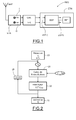
- the reference REC designates a multi-standard receiver capable of processing signals compatible with different transmission standards, such as the WiMAX and WiFi standards.
- this reception platform REC comprises an antenna ANT capable of receiving an incident signal compatible with one of the transmission standards.
- An ETA analog processing stage is connected to the antenna ANT and comprises, in particular, mixers capable of performing a frequency transposition for bringing back, for example, the analog baseband signal according to two quadrature processing channels, namely the channel. "I" (in phase) and the "Q” channel (in phase quadrature) according to a conventional name and known to those skilled in the art.
- analog processing stage is coupled an analog / digital conversion stage CAN, preferably of the delta-sigma type.
- analog / digital conversion stage CAN preferably of the delta-sigma type.
- the structure of such a delta-sigma analog / digital conversion stage is conventional and well known to those skilled in the art.
- a digital processing stage ETN is coupled to the output of the analog / digital conversion stage CAN and comprises in particular a DCF sampling frequency conversion device followed by other processing modules, for example an FFT Fourier transform module, produced for example in a processor, commonly called by the skilled person "processor baseband processing ".
- the sampling frequency of the digital analog converter is not necessarily a multiple of the sampling frequency required for the FFT block and specified by the standards.
- the sampling frequency conversion device DCF may be capable of performing a frequency decimation, that is to say a down-conversion of sampling frequency, in a non-integer ratio. , and not necessarily a rational relationship.
- This conversion ratio can therefore be a non-integer real number greater than 1 although integers greater than 1 are also possible.
- the device DCF comprises selection means capable of selecting the conversion ratio F s / F i in a set of predetermined values, for example the set of values mentioned below. above.
- the frequency F s denotes the sampling frequency of the signal upstream of the DCF device, and is also hereinafter referred to as the "first sampling frequency", whereas F i designates the sampling frequency of the digital signal. delivered by the DCF device, also called “second sampling frequency”.
- This sampling frequency F s is very much greater than B / 2, for example of the order of ten to fifteen times B / 2.
- y i (nT i ) denotes the digital signal sampled at frequency F i after conversion of the sampling frequency.
- this sampling rate conversion is effected from, in particular, an interpolation filter.
- h I (t) the impulse response of the interpolation filter in the time domain.
- the frequency spectrum X (f) of the input signal is periodic with a period F s , which means that there are replicas of the signal at frequencies spaced from F s .
- the filtering operation is equivalent to a discrete sum.
- the samples of the input signal will be designated by x k and the output samples will be designated y n .
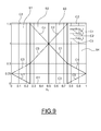
- the input samples are received (step 20) at the first sampling frequency F s .
- Output samples y n corresponding to the second sampling frequency F i are generated from the input samples and an interpolation filter whose time domain impulse response is equal to h I.
- the ratio F s / F i is strictly greater than 1 and is for example a non-integer, rational or irrational number.
- the elaboration of the output samples comprises, for each current input sample x k , the update (step 22) of the current values of N successive output samples with N contributions respectively calculated (step 21) from the value of the current input sample x k weighted by the values of N coefficients of the filter h1, ... hN, associated with this current input sample. It should be noted here that the number N is fixed and identical for all the input samples x k , whatever the value of the ratio F s / F i .
- delivery 23 of an output sample y n whose value has been updated with a contribution from a current input sample x k is carried out if output sample shall not receive a contribution from the following input sample x k + 1 .
- the actual value of this output sample delivered is the value updated with the contribution from the current input sample x k .
- steps 21 and 22 are repeated for the sample x k + 1 (step 24).
- n produces 30 of the value of the current input sample x k by the value h j of the corresponding coefficient of the filter.
- step 32 After updating the sample y n with this contribution, it is determined (step 32) whether or not the next input sample x k + 1 should contribute to the value of the output sample y n .
- the output sample y n is delivered with its effective value equal to its last updated value. If the answer is yes, the new input will be calculated for the next input sample x k + 1 (step 34) in a manner similar to that just described for the current input sample x k .
- the width of the impulse response of the interpolation filter sets the value of the number N.
- cm denotes a multiplier coefficient, not necessarily integer
- T i the second time period corresponding to the second sampling frequency F i
- the interpolation filter has a bandwidth equal to 2.5.T i .
- the number N is therefore equal to 3, that is to say that each input sample will contribute to the update of three output samples.
- h I (t) is an even function (i.e., h I (t) is equal to h I (-t) and h I (t) is equal to zero if t does not belong to the interval [-3 T i / 2; 3 T i / 2]).
- the determination of the time position of a current input sample x k with respect to the N interpolation time instants t n , ..., t n + N-1 comprises the determination of a time interval ⁇ k between the first time instant associated with the current input sample x k and one of the N interpolation time instants, for example the previous interpolation time instant.
- the temporal moment of previous interpolation is the instant t n + 1 , while it is the moment t n in the configuration illustrated on the figure 5 .
- the values of the N coefficients of the filter h1, ... hN with which the N contributions of the current input sample x k are calculated will be determined (step 61).
- the calculation of the coefficients h1, h2 and h3 depends on the position of ⁇ k with respect to the value 0.5.
- (1 + ⁇ k ) and (1- ⁇ k ) represent two other time intervals respectively between the instant of arrival of the current sample x k , and the other time instants of interpolation t n and t n + 2 .
- ⁇ k h I (1 + ⁇ k )
- h2 h I ( ⁇ k )
- h2 h I (1- ⁇ k )
- h3 h I (2- ⁇ k )
- step d It is then checked (step d) if the output sample y n is ready to be delivered with its effective value, that is to say whether or not it should receive a contribution from the next input sample x k + 1 .
- the output sample y n is outputted and, as will be seen in more detail, the registers to which the output samples are assigned and in which the sample is accumulated are shifted. output considered the different contributions from different input samples.
- condition CD1 ie if the output sample is not ready to be issued because it will receive a contribution from the following input sample x k +1 , we repeat steps a) to d) which have just been described, for the next sample x k + 1 .
- analog / digital converter CAN is a delta-sigma type converter
- a cardinal sinus function for the amplitude / frequency response curve of the filter.
- sinc cardinal sinus function
- Several solutions are possible depending on the level of attenuation desired.
- One can in this respect use either a simple function sinc, the product of a function sinc by a function cosine, a function sinc2 (cardinal sinus squared) or the product of a function sinc2 by a function cosine, or else a function sinc3 (cardinal sinus raised to the cube) or the product of this function sinc3 by a cosine function or else other functions combining or not the cardinal sinus function.
- H I (f) sin vs ⁇ f F i 2 . cos 2 ⁇ ⁇ ⁇ f 4 ⁇ F i
- this function may comprise at least one linear zone.
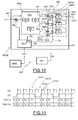
- the curve C1 represents the evolution of the coefficient h1 as a function of ⁇ k .
- Curve C2 represents the evolution of h2 coefficient ⁇ as a function of k and curve C3 represents the evolution of coefficient h3 according to ⁇ k. We see that these curves are formed of linear zones, in this case segments of straight lines.
- the logical value R k designates, according to its value, the four sectors corresponding to the ranges of values of ⁇ k .
- the only multiplication performed is on a small number of bits.
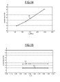
- the DCF device comprises a reception input MR adapted to receive the samples x k of the digital signal, MELB production means able to produce the output samples y n , and output means SO1 able to deliver these output samples y n .
- the device DCF further comprises selection means MSEL able to select the value of the ratio F s / F i from a set of predetermined values corresponding to sampling rate values compatible with several different standards, for example the WiMAX standards or Wireless. It should be noted here that the selection means MSEL actually select the opposite of this ratio.
- the MELB production means comprise calculating means MCL able to calculate the N contributions of each input sample x k , and processing means able to update the values of the output samples.
- the calculation means MCL comprise first means able to determine the temporal position of a current input sample with respect to the N interpolation time instants respectively associated with the N output samples to be updated, and second means able to determine the values of the N filter coefficients from of this temporal position.
- the temporal position is determined via the parameter ⁇ ' k .
- the first means comprise a numerically controlled oscillator NCO capable, from the periods T s and T i , and a a clock signal CK of period T s , delivered by a quartz QZT for example, to determine the parameter ⁇ ' k for a current input sample x k .
- the calculation means MCL furthermore comprise a multiplier ML receiving on the one hand the current sample x k and on the other hand, the parameter ⁇ ' k .
- the output of the multiplier and the sample x k are connected to two inputs of a BLC block comprising adders ADD, subtracters SB, and bit shift means SH, all of these means being individually selectable according to the value the time interval ⁇ k , that is to say according to the logic parameter R k delivered by the NCO oscillator.
- the calculation of the values of the filter coefficients and the calculation of the contributions are done globally within the BLC block.
- the processing means may also be three adders ADD1, ADD2, ADD3, each having a first input EA1 coupled to the corresponding input of the processing means (IN1, IN2 or IN3) and a second input EA2.
- the processing means also comprise three multiplexers MUX1, MUX2, MUX3 capable of being controlled by control means MC functionally incorporated within the NCO oscillator, and each having a first input EMX1 connected to the output SA of the corresponding adder , and a second EMX2 input.
- the processing means also comprise a chain of three registers R1, R2, R3 each having an input ER1 coupled to the output of the corresponding multiplexer and an output SR1 coupled to the second input EA2 of the corresponding adder.
- the output of the last register of the chain in this case the register R1, is coupled to the output SO1, while the output of each of the other registers R2, R3 is coupled to the second input of the multiplexer associated with the next register in said chain of registers. More specifically, the output of the register R3 is coupled to the second input of the multiplexer MUX2 while the output of the register R2 is coupled to the second input of the register MUX1.
- the processing means also comprise an auxiliary register RGA containing a datum of zero value and whose output is coupled to the second input of the multiplexer MUX 3 associated with the first register R3 of the string.
- the device DCF is clocked at the rhythm of the clock signal CK, an input sample x k arriving for example at each rising edge of the clock signal CK.
- the control signal DS which controls the multiplexers of the processing means takes the value 1, which connects the first input of the multiplexers to their output, and thus loops the output of each of the registers to the second input of the corresponding adder. This makes it possible to accumulate in each of the registers the corresponding contribution and to update the corresponding value of the output sample ( figure 12 ).
- the NCO oscillator determines by applying the condition CD1 mentioned above, if the sample y n must or not be output. If this is not the case, a logic signal DV takes the value "0", indicating that the output of the register R1 is not valid data.
- output samples of rank n to n + 2 are updated and, in this respect, the three output samples are respectively assigned the three registers R1, R2 and R3 in each of which we accumulate for the sample of output considered, the different contributions from the different input samples.
- the value contained in the register R1 is delivered and the registers R1 and R2 are assigned to the samples y n + 1 and y n + 2 , while the register R3 is assigned the sample output y n + 3 .
- the register R3 is initialized to a chosen initialization value, in this case the value "0".
- This register shift is effected by means of the control signal DS which takes the value "0" for example, and which makes it possible to connect the second inputs of the multiplexers to their corresponding outputs ( figure 13 ).
- edges of the DV signal are slightly shifted with respect to the rising edge of the clock signal CK.
- sample y 4 (on channel I and on channel Q) is ready to be delivered on the first rising edge of clock signal CK, which results in the rise to "1" of the DV signal.
- the sample y 5 is updated and is ready to be issued. Accordingly, the DV signal remains "1" and the sample 5 there will be issued on the next rising edge of clock signal CK.
- the sample y 6 is further updated and is also ready to be delivered on the next rising edge of the clock signal CK.
- the DV signal is always at "1".
- next output sample y 7 is still in development.
- the sample y 7 is not ready to be issued because its preparation requires the input of a subsequent input sample.
- the signal DV thus falls back to "0" and remains at this value during the next cycle CYC8, during which the development of the output sample y 7 is continued by updating its value with two other contributions coming respectively from the two following input samples. It is only at the end of cycle CYC8 that the sample y 7 is ready to be delivered, which will occur on the rising edge FM8 of the clock signal CK.
- the DV signal then resumes the value "1".
- the sample y 8 will be delivered.
- the sample y 9 will also be updated during the cycle CYC9 But this sample will still require two clock cycles of the CK signal to be updated before being issued. Then the sample is 10 and the sample 11 there will require still respectively one and two signal CK of clock cycles to be updated before being issued.
- the output samples y n are delivered at the rate of the rising edges of the clock signal CK, but on only some of these rising edges as a function of the number of contributions required for each of the output samples y n .
- the number of contributions is different for the output samples. Each contribution number depends on N, the conversion ratio and also on ⁇ k (see condition CD1 above). In general the number of contributions is greater than or equal to N, and in practice much greater than N.
- the output frequency of the output samples is therefore different from the sampling frequency F i .
- the output samples y n are effectively representative of a sampling of the digital signal at a frequency F i .
- Simulations show that the power consumption of a frequency conversion device according to aspects of the invention varies substantially linearly with the first sampling frequency F s .
- this consumed power is substantially constant whatever the value of the conversion ratio F s / F i , whereas in the solutions of the prior art providing for a storage of filter coefficients for each conversion ratio envisaged, the power consumed increases as the value of the conversion ratio increases.
- the curve C4 illustrates the substantially linear progression of the power as a function of F s .
- the curve C5 illustrates the substantially constant nature of the power as a function of the conversion ratio, for a frequency F s equal to 60 MHz, while the curve C6 is plotted for a frequency F s equal to 120 MHz.
- a substantially constant power of the order of 8 mW would be obtained.
Landscapes
- Physics & Mathematics (AREA)
- Engineering & Computer Science (AREA)
- Computer Hardware Design (AREA)
- Mathematical Physics (AREA)
- Compression, Expansion, Code Conversion, And Decoders (AREA)
Priority Applications (2)
| Application Number | Priority Date | Filing Date | Title |
|---|---|---|---|
| EP08151565A EP2091149A1 (de) | 2008-02-18 | 2008-02-18 | Verfahren und Vorrichtung zur Abwärtsumwandlung der Abtastfrequenz eines digitalen Signals. |
| US12/372,258 US8249208B2 (en) | 2008-02-18 | 2009-02-17 | Method and device for downconverting the sampling frequency of a digital signal, for example in a non-integer frequency ratio |
Applications Claiming Priority (1)
| Application Number | Priority Date | Filing Date | Title |
|---|---|---|---|
| EP08151565A EP2091149A1 (de) | 2008-02-18 | 2008-02-18 | Verfahren und Vorrichtung zur Abwärtsumwandlung der Abtastfrequenz eines digitalen Signals. |
Publications (1)
| Publication Number | Publication Date |
|---|---|
| EP2091149A1 true EP2091149A1 (de) | 2009-08-19 |
Family
ID=39769445
Family Applications (1)
| Application Number | Title | Priority Date | Filing Date |
|---|---|---|---|
| EP08151565A Withdrawn EP2091149A1 (de) | 2008-02-18 | 2008-02-18 | Verfahren und Vorrichtung zur Abwärtsumwandlung der Abtastfrequenz eines digitalen Signals. |
Country Status (2)
| Country | Link |
|---|---|
| US (1) | US8249208B2 (de) |
| EP (1) | EP2091149A1 (de) |
Families Citing this family (3)
| Publication number | Priority date | Publication date | Assignee | Title |
|---|---|---|---|---|
| US8693897B2 (en) | 2011-01-22 | 2014-04-08 | Viasat, Inc. | Digital demodulator architecture |
| US8705664B2 (en) * | 2011-01-22 | 2014-04-22 | Viasat, Inc. | Soft-input generation for soft-decision FEC decoding |
| JP6219117B2 (ja) * | 2013-10-09 | 2017-10-25 | 株式会社Nttドコモ | ユーザ端末、無線基地局及び無線通信方法 |
Citations (2)
| Publication number | Priority date | Publication date | Assignee | Title |
|---|---|---|---|---|
| EP0881764A2 (de) * | 1997-05-30 | 1998-12-02 | Commquest Technologies, Inc. | Verfahren und Gerät für unterabstastende Filter mit veränderlicher Datenrate für zeitdiskrete Abtastsysteme mit fester Abtastrate |
| DE10015700A1 (de) * | 2000-03-27 | 2001-10-11 | Univ Dresden Tech | Verfahren und Schaltungsanordnung zur Abtastratenwandlung digitaler Signale |
Family Cites Families (6)
| Publication number | Priority date | Publication date | Assignee | Title |
|---|---|---|---|---|
| JP3707148B2 (ja) * | 1996-08-21 | 2005-10-19 | ヤマハ株式会社 | サンプリング周波数変換方法およびサンプリング周波数変換装置 |
| US5892694A (en) * | 1997-05-01 | 1999-04-06 | Vlsi Technology, Inc. | Sample rate conversion between asynchronous digital systems |
| US6259389B1 (en) * | 1998-11-20 | 2001-07-10 | General Electric Company | System for designing and testing a sigma-delta modulator using response surface techniques |
| DE10257666A1 (de) * | 2002-12-10 | 2004-08-05 | Infineon Technologies Ag | Empfangsanordnung eines schnurlosen Kommunikationssystems |
| SG126799A1 (en) * | 2005-04-29 | 2006-11-29 | Oki Techno Ct Singapore Pte Ltd | A modified transposed farrow structure |
| FR2886076B1 (fr) * | 2005-05-23 | 2007-10-19 | Anagram Technologies Sa | Procede et dispositif de conversion de frequence d'echantillonnage d'un signal numerique |
-
2008
- 2008-02-18 EP EP08151565A patent/EP2091149A1/de not_active Withdrawn
-
2009
- 2009-02-17 US US12/372,258 patent/US8249208B2/en not_active Expired - Fee Related
Patent Citations (2)
| Publication number | Priority date | Publication date | Assignee | Title |
|---|---|---|---|---|
| EP0881764A2 (de) * | 1997-05-30 | 1998-12-02 | Commquest Technologies, Inc. | Verfahren und Gerät für unterabstastende Filter mit veränderlicher Datenrate für zeitdiskrete Abtastsysteme mit fester Abtastrate |
| DE10015700A1 (de) * | 2000-03-27 | 2001-10-11 | Univ Dresden Tech | Verfahren und Schaltungsanordnung zur Abtastratenwandlung digitaler Signale |
Non-Patent Citations (1)
| Title |
|---|
| RAMSTAD T A: "DIGITAL METHODS FOR CONVERSION BETWEEN ARBITRARY SAMPLING FREQUENCIES", IEEE TRANSACTIONS ON ACOUSTICS, SPEECH AND SIGNAL PROCESSING, IEEE INC. NEW YORK, USA, vol. ASSP-32, no. 3, 1 June 1984 (1984-06-01), pages 577 - 591, XP002025612, ISSN: 0096-3518 * |
Also Published As
| Publication number | Publication date |
|---|---|
| US8249208B2 (en) | 2012-08-21 |
| US20090207959A1 (en) | 2009-08-20 |
Similar Documents
| Publication | Publication Date | Title |
|---|---|---|
| EP3161659B1 (de) | Wiederabtastung eines tonsignals durch interpolation zur codierung/decodierung mit geringer verzögerung | |
| CH674435A5 (de) | ||
| EP2460275B1 (de) | Korrektur von analogdefekten bei parallelen analog-digital-wandlern, insbesondere zur anwendung in multistandard-, softwaredefiniertem und/oder kognitivem funk | |
| FR2702902A1 (fr) | Récepteur numérique à fréquence intermédiaire et procédé de filtrage en bande de base mis en Óoeuvre dans ce récepteur. | |
| FR2644022A1 (fr) | Dispositif de telemetrie avec un poste emetteur utilisant un filtre recurrent pour limitation de la largeur de bande | |
| FR3002391A1 (fr) | Procede et dispositif pour notamment compenser le desappariement des decalages d'horloges de plusieurs convertisseurs analogiques/numeriques temporellement entrelaces | |
| WO2013007613A1 (fr) | Procédé et module d'estimation de bias fréquentiel dans un système télécommunications numériques | |
| EP2091149A1 (de) | Verfahren und Vorrichtung zur Abwärtsumwandlung der Abtastfrequenz eines digitalen Signals. | |
| EP3729299B1 (de) | Digitaler interpolationsfilter, entsprechende rhythmuswechselvorrichtung und empfangsvorrichtung | |
| EP0970562B1 (de) | Digitalfilter für fraktionale verzögerungen | |
| US20020190886A1 (en) | New method and a system of acquiring local signal behavior parameters for representing and processing a signal | |
| EP1940023A2 (de) | Kaskadierbare, digitale Filterbank und darin enthaltene Empfangsschaltung | |
| CN102209057A (zh) | 信号接收器与估计残余多普勒频率的方法 | |
| FR2485304A1 (fr) | Dispositif de traitement audiofrequence de ligne d'abonne | |
| WO2002015406A1 (en) | Acquiring local signal behavior parameters | |
| FR2817100A1 (fr) | Procede pour optimiser les performances d'un emetteur pour systeme de radiocommunications mobiles | |
| EP1101283B1 (de) | Verfahren zur herstellung von digitalen nyquist filtern ohne störungen zwischen symbolen und entsprechende filteranordnung | |
| FR2911453A1 (fr) | Procede et dispsitif de traitement d'un signal incident, en particulier de transposition de frequence. | |
| FR3142638A1 (fr) | Récepteur fréquence radio | |
| EP1315346B1 (de) | Verfahren und Vorrichtung für Blockentzerrung mit verbesserter Interpolation | |
| FR2911462A1 (fr) | Procede et dispositif de filtrage et de conversion analogique/numerique d'un signal analogique. | |
| FR3152934A1 (fr) | Procédé de calcul de coefficients de compensation d'une chaine de réception analogique, dispositif et programme correspondant | |
| FR2911461A1 (fr) | Procede et dispositif de filtrage et de conversion analogique/numerique d'un signal analogique | |
| FR2911452A1 (fr) | Procede et dispositif de traitement d'un signal incident, en particulier de transposition de frequence | |
| BE890775A (fr) | Convertisseur analogique-numerique a interpolation |
Legal Events
| Date | Code | Title | Description |
|---|---|---|---|
| PUAI | Public reference made under article 153(3) epc to a published international application that has entered the european phase |
Free format text: ORIGINAL CODE: 0009012 |
|
| AK | Designated contracting states |
Kind code of ref document: A1 Designated state(s): AT BE BG CH CY CZ DE DK EE ES FI FR GB GR HR HU IE IS IT LI LT LU LV MC MT NL NO PL PT RO SE SI SK TR |
|
| AX | Request for extension of the european patent |
Extension state: AL BA MK RS |
|
| 17P | Request for examination filed |
Effective date: 20100114 |
|
| 17Q | First examination report despatched |
Effective date: 20100209 |
|
| AKX | Designation fees paid |
Designated state(s): DE FR GB |
|
| STAA | Information on the status of an ep patent application or granted ep patent |
Free format text: STATUS: THE APPLICATION IS DEEMED TO BE WITHDRAWN |
|
| 18D | Application deemed to be withdrawn |
Effective date: 20130903 |