EP2092429B1 - Konfigurierbarer cache für einen mikroprozessor - Google Patents
Konfigurierbarer cache für einen mikroprozessor Download PDFInfo
- Publication number
- EP2092429B1 EP2092429B1 EP07855101A EP07855101A EP2092429B1 EP 2092429 B1 EP2092429 B1 EP 2092429B1 EP 07855101 A EP07855101 A EP 07855101A EP 07855101 A EP07855101 A EP 07855101A EP 2092429 B1 EP2092429 B1 EP 2092429B1
- Authority
- EP
- European Patent Office
- Prior art keywords
- cache
- cache line
- instruction
- line
- address
- Prior art date
- Legal status (The legal status is an assumption and is not a legal conclusion. Google has not performed a legal analysis and makes no representation as to the accuracy of the status listed.)
- Active
Links
Images


Classifications
-
- G—PHYSICS
- G06—COMPUTING OR CALCULATING; COUNTING
- G06F—ELECTRIC DIGITAL DATA PROCESSING
- G06F12/00—Accessing, addressing or allocating within memory systems or architectures
- G06F12/02—Addressing or allocation; Relocation
- G06F12/08—Addressing or allocation; Relocation in hierarchically structured memory systems, e.g. virtual memory systems
- G06F12/0802—Addressing of a memory level in which the access to the desired data or data block requires associative addressing means, e.g. caches
- G06F12/0893—Caches characterised by their organisation or structure
- G06F12/0895—Caches characterised by their organisation or structure of parts of caches, e.g. directory or tag array
-
- G—PHYSICS
- G06—COMPUTING OR CALCULATING; COUNTING
- G06F—ELECTRIC DIGITAL DATA PROCESSING
- G06F12/00—Accessing, addressing or allocating within memory systems or architectures
- G06F12/02—Addressing or allocation; Relocation
- G06F12/08—Addressing or allocation; Relocation in hierarchically structured memory systems, e.g. virtual memory systems
- G06F12/0802—Addressing of a memory level in which the access to the desired data or data block requires associative addressing means, e.g. caches
- G06F12/0875—Addressing of a memory level in which the access to the desired data or data block requires associative addressing means, e.g. caches with dedicated cache, e.g. instruction or stack
-
- G—PHYSICS
- G06—COMPUTING OR CALCULATING; COUNTING
- G06F—ELECTRIC DIGITAL DATA PROCESSING
- G06F13/00—Interconnection of, or transfer of information or other signals between, memories, input/output devices or central processing units
-
- G—PHYSICS
- G06—COMPUTING OR CALCULATING; COUNTING
- G06F—ELECTRIC DIGITAL DATA PROCESSING
- G06F9/00—Arrangements for program control, e.g. control units
- G06F9/06—Arrangements for program control, e.g. control units using stored programs, i.e. using an internal store of processing equipment to receive or retain programs
Definitions
- the present invention concerns a configurable cache for a microprocessor or microcontroller.
- US 2002/116567 discloses a cache module for a central processing unit comprising a cache control unit coupled with a memory, a cache memory coupled with said control unit and said memory, wherein said cache memory comprises a plurality of cache lines, at least one cache line of said plurality of cache lines comprises an address tag bit field and an associated storage area for storing instructions to be issued sequentially.
- Small microcontroller designs are limited in the amount of cache that can be on chip and they cannot support the large sizes of high latency but high throughput narrow memory. Thus, a need for a configurable cache for a microcontroller or microprocessor exists.
- a cache module for a central processing unit may comprise a cache control unit coupled with a memory, and a cache memory coupled with the control unit and the memory, wherein the cache memory comprises a plurality of cache lines, at least one cache line of the plurality of cache lines comprises an address tag bit field and an associated storage area for storing instructions to be issued sequentially and at least one control bit field, wherein the control bit field is coupled with the address tag bit field to mask a predefined number of bits in the address tag bit field.
- a microcontroller may comprise a central processing unit; a cache module coupled with the central processing unit comprising: a cache control unit coupled with a memory, and a cache memory coupled with the control unit and the memory, wherein the cache memory comprises a plurality of cache lines, at least one cache line of the plurality of cache lines comprises an address tag bit field and an associated storage area for storing instructions to be issued sequentially and at least one control bit field, wherein the control bit field is coupled with the address tag bit field to mask a predefined number of bits in the address tag bit field.
- the at least one cache line further may comprise at least one locking bit for locking of the associated cache line.
- each cache line may comprise at least one locking bit for locking of the associated cache line.
- each cache line further may comprise at least one branch trail bit for automatic locking of the associated cache line, wherein in case the branch trail bit is set the locking bit is automatically set in case a predefined branch instruction in the associated storage area has been issued.
- each cache line further may comprise a validity control bit for indicating the validity of the associated cache line.
- each cache line further may comprise a type control bit for indicating whether the cache line is used as an instruction cache line or a data cache line.
- the cache module may further comprise a prefetch unit coupled with the memory and the cache memory, wherein the prefetch unit is operable to load instructions from the memory into another cache line wherein the instructions are sequential to instructions which are currently issued from the cache line.
- a least recently used algorithm may be used to determine which cache line is to be overwritten.
- a method of operating a cache having a plurality of cache lines for a central processing unit may comprise the steps of storing a plurality of sequential instructions within a cache line of the cache and an associated start address of the sequential instructions in an associated address tag bit field of the cache line; storing a mask in a mask bit field of the cache line; receiving an instruction address request; comparing the instruction address request to generate a hit or miss signal with a partial address generated by masking the associated address tag bit field with the mask bit field; accessing an instruction from the cache line if a hit signal has been generated.
- the instruction address request may be generated by an interrupt or by a trap instruction.
- the interrupt or trap instruction may generate an address that consists of a base address and an offset address, wherein the offset is generated by an interrupt priority or by a trap number, respectively.
- the method may further comprise the step of locking the cache line.
- the method may further comprise the steps of storing a plurality of sequential instructions within another cache line of the cache; setting a branch trail function for the another cache line; executing instructions fetched from the another cache line; automatically locking the another cache line upon calling a subroutine.
- the method may further comprise the step of resetting the branch trail function for the another cache line upon a return from the subroutine.
- the subroutine may be called upon execution of an instruction contained in the another cache line.
- Standard microcontroller units usually comprise an 8-bit or 16-bit microprocessor core. Only recently have 32-bit core entered into the MCU arena. All these cores usually do not have Caches. Only complex high end 32-bit microcontrollers may have caches. This is because caches are large and costly for MCU.
- the disclosed embodiments provide for a middle ground of a small configurable cache that is configurable on the fly and may act as a prefetch and branch trail buffer while providing the optimal cache depth for MCU applications.
- a cache can be designed to be configurable to operate very flexible. For example, it can be programmed to operate strictly as a cache, which is useful for small loop optimization. To this end, respective cache lines comprising the loop can be manually locked. It can also dedicate a certain number of cache lines, for example, up to half the lines for Linked Branch History storage, which can accelerate function call returns. Finally, it can be configured to prefetch sequential program information into the least recently used cache line when a first instruction is issued from a cache line. By prefetching program instructions at twice the rate the microprocessor can use them, the memory system provides available bandwidth to fetch program data without stalling program instruction flow. In practice, not all program data fetches are transparent.
- the cache design approach according to different embodiments provides a mechanism to improve performance by giving a balance of feature of a low latency cache combined with a high latency but high throughput wide memory.
- a cache can be designed to be a runtime and on-the-fly configurable fully associative cache.
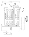
- Fig. 1 shows a block diagram of an embodiment of such a configurable cache 100.
- Coupling busses 110a and 110b couple the cache to a central processing unit (CPU) of a microcontroller or microprocessor.
- the cache 100 comprises a cache controller 120 which is coupled to the instruction cache section 130 and the data cache section 140.
- Each instruction cache section comprises the instruction memory proper and associated control bits and tags, for example, in form of lines wherein a line may include a storage area for storing a plurality of words. For example, a word can be 16 bits long and a line within the instruction cache 130 may have 4 double words resulting in 4 x 32 bits.
- an small instruction cache 130 may include 4 such lines. According to other embodiments, other configuration depending on the design of the respective processor might be more advantageous.
- a data cache section 140 can be designed similar to the instruction cache design 130. Depending on the design model, separate data and instruction cache sections 130 and 140 may be desirable as for example useful in a processor having a Harvard architecture. However, in a conventional von Neumann type microprocessor, a mixed cache capable of caching instructions and data from the same memory may be used.
- Fig. 1 only shows a program flash memory 160 (PFM) connected to the instruction and data cache 130, 140 according to a processor with a Harvard architecture.
- PFM program flash memory 160
- a data memory can be coupled separately in a Harvard architecture or memory 160 may be a unified instruction/data memory as used in a von Neumann architecture.
- a multiplexer 150 is controlled, for example, by the cache controller 120 and provides the data/instruction stored in the cache memory 130, 140 to the CPU via bus 110b.
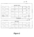
- Fig. 2 shows the structure of an instruction cache 130 and data cache according to an embodiment in more detail.
- the arrangement again shows separate caches for instruction and data.
- Each line of a cache comprises a data/instruction Storage Area and a plurality of an associated control and tag bits, for example, IFM, TAG, and BT.
- IFM designates a particular mask which can be used, for example, to mask certain bits of the address tag field TAG which contains the start address of the data/instruction cache DATA as will be explained in more detail below.
- Each line can, for example, comprises 4 x 32 bits of instruction/data cache as shown in Fig. 2 .
- the tag field may comprise the actual address as well as additional bits indicating validity of the respective cache line, locking, type, etc.
- a branch tail bit BT is provided for each cache line.
- the CPU can automatically lock the associated cache line whenever a subroutine call instruction is executed within the respective cache line and that instruction is not the last instruction in the line. In such a case, the respective cache line is automatically locked and the instructions following the respective call instruction will be present in the cache when the program returns from the respective subroutine as will be explained in more detail below.
- Fig. 3 shows another embodiment of a configurable cache.
- Cache controller 120 provides control signals and information for all functions of the cache.
- cache controller 120 controls a TAG logic 310 which is coupled with a Hit logic 320 that also processes data from cache controller 120 and from a pre-fetch tag 330 that is provided by the cache controller.
- the hit logic generates a signal that controls the cache line address encoder 340 which addresses the cache memory 350 which in this embodiment comprises, for example, 16 lines of data/instruction memory each line comprising, for example, 4 x 32 bit double words for instruction/data storage.
- the program flash memory 160 is coupled with the cache controller 120 and with the cache via a pre-fetch unit 360 that is also connected to the cache line address encoder 340.
- the pre-fetch unit 360 transfers instructions into each cache line of cache memory 350 as addressed by the cache line address encoder 340 either directly or through a buffer.
- pre-fetch unit 360 may comprise one or more buffers capable of storing the instruction to be transferred into the storage area of a respective cache line.
- Multiplexer 150 is controlled to select the respective byte/word/double word within cache memory 350 or from the prefetch buffer of unit 360 and provide it to the CPU bus 110b.
- Fig. 4 shows the cache memory 350 in more detail.
- 16 cache lines are provided.
- Each line comprises a plurality of control bits, and a 4 x 32 Bit instruction/data storage area (Word0 - Word3).
- the control bits comprise a mask MASK, an address tag TAG, a validity bit V, a lock bit L, a type bit T, and a branch trail bit BT.
- the mask MASK provides for masking selected bits of the address tag TAG during a comparison by the hit logic 320 as will be explained in more detail below.
- the address tag TAG thereby indicates the beginning of the cache line in memory 160.
- the address tag TAG is readable and writeable and when written by a user will force a pre-fetch function.
- Validity bit V indicates that the entries in the associated cache line are valid. This bit cannot be altered by a user and is set or reset automatically.
- Lock bit L indicates whether the cache line is locked and, thus, cannot be overwritten. This bit can be altered by a user or can be set automatically with respect to the branch trail function as explained below.
- Bit T indicates the type of cache line, i.e. whether the cache line is used as an instruction cache line or as a data cache line. This bit may be designed to be altered by a user which allows for a very flexible assignment and configuration of a cache.
- a general configuration register can be used, to define a certain number of lines that will be used to cache data whereas the remaining cache lines will be used for instruction caching.
- Bits T may still be provided to indicate which cache lines are set to be designated data cache lines and therefore cannot be altered in such an embodiment.
- the cache according to one embodiment can be, for example, configured to dedicate no cache lines, 1, 2, or 4 cache lines for data cache purposes. Such an assignment can thus split the cache into two parts, for example, data cache lines can be assigned from the bottom of the cache upwards depending on the number of assigned lines. Other configurations with more data cache lines are of course possible and dependent on the respective design of the cache. Hence, when set, bit T indicates that this line is used for data caching.
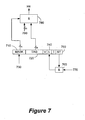
- Fig. 7 shows an embodiment of some logic circuitry that can be used to implement the branch trail function.
- the branch trail bit 750 is, as explained above, used to automatically lock the associated cache line in case a subroutine instruction, trap, interrupt, or other instruction that will branch away to a subroutine and will return is executed within the cache line and is not the last instruction in the line.
- the CPU can automatically lock the associated line by setting bit 740 through logic gate 760 when a call subroutine type instruction has been executed and the program branches away from its linear execution sequence.
- the execution of such a subroutine type instruction can be detected in the execution unit and signaled to logic gate 760 by signal 770.
- This functionality is enabled when at least one instruction is remaining in the cache line that has not been executed yet but will be executed when the program returns from the respective subroutine. In case such an instruction is placed in the last memory space of a cache line there would be no point in keeping the cache line automatically locked because the following instruction will be in a different cache line or may not even be in the cache yet.
- the CPU sets and resets the lock bit 740 automatically when bit 750 is set depending on the execution of the respective subroutine or interrupt call which is signaled to logic gate 760 by detection signal 770.
- Fig. 5 and 6 show examples of a general cache control register 510 and other control registers 610-660 implemented within a microprocessor or microcontroller to control the behavior and functionality of the configurable cache.
- All registers can be designed as 32 bit register for use in a 32 bit environment. However, these registers can be easily adapted to work in a 16 or 8 bit environment.
- register CHECON comprises bit 31 to enable or disable the entire cache and bit 16 CHECOH can be used to provide for a cache coherency setting on a PFM program cycle bit.
- this bit CHECOH can invalidate all data and instruction lines when set or can invalidate all data lines and only instruction lines that are not locked.
- Bit 24 can be used to enable a forced data cache function as will be explained in more detail below.
- Bits 11-12 BTSZ can be used to enable/disable branch trail tagging. For example, in one embodiment, if enabled the branch trail tagging can be set to a size of 1, 2, or 4 lines. Thus, 1, 2, or 4 cache lines will have this functionality. According to other embodiments, all cache lines may be enabled for such a functionality. Bits 8-9 DCSZ are used to define the number of data cache lines as explained above. In one embodiment, the number can be set to enable zero, 1, 2, or 4 data cache lines.
- Bits 4-5 PREFEN can be used to enable predictive prefetch selectively for cacheable and non-cacheable regions of the memory.
- a cacheable region of a memory can be a region within the memory such as memory or program regions that can be actually cached meaning a memory region that is actually coupled with the cache.
- Non-cacheable regions generally refer, for example, to memory-mapped peripheral space which usually cannot be cached. The distinction between cacheable and non-cacheable regions depends on the system design. Some embodiments might require such a distinction and respective microprocessor/microcontroller will supports cached and non-cached methodologies whereas other embodiments of processor may be able to cache any type of memory whether they are actual memory regions or memory mapped regions.
- the prefetch unit will always fetch the instructions following a cache line from which an instruction is currently issued.
- Using two bits allows, for example, for four different settings, such as, enable predictive prefetch for both cacheable and non-cacheable regions, enable predictive prefetch for non-cacheable regions only, enable predictive prefetch for cacheable regions only, and disable predictive prefetch.
- a cache line comprises 16 bytes or four double words. If the central processing unit, for example, requests instruction x1 from address 0x001000, the cache control logic compares all address tags with 0x00100X (wherein bits X are ignored). If the controller generates a hit, the respective line is selected. The selected line comprises all instructions starting with address 0x001000.
- the prefetch unit will be triggered to prefetch the next line of instructions.
- the prefetch unit will calculate the following address tag as 0x001010 and start loading the respective instructions in the next available cache line.
- the central processing unit further executes instructions from addresses 0x001004, 0x001008, and 0x00100C
- the prefetch unit fills up the next available cache line with instructions from addresses 0x001010, 0x001014, 0x001018, and 0x00101C.
- the prefetch unit will be done with loading up the next instructions. Thus, central processing unit will not be stalled.
- Bits 0-2 are used to define the number of wait states of a program flash memory.
- a wide variety of different flash memories can be used with the microcontroller.
- Each line within a cache as shown in Fig. 4 may be mapped under control to registers as shown in Fig. 6 .
- a cache line can be designed to fully accessible through read and write operations and can be fully altered by a user.
- some bits of a cache line may be designed not to be altered by a user or may require an unlocking of the respective line before a user can alter the respective line.
- an index register 600 can be provided for selecting one of the 16 cache lines. Once a cache line has been selected through the index register 600, the cache line is accessible through the following registers 610-660.
- a mask register may comprise, for example, in bits 5-15 the mask MASK of the selected cache line.
- a second register for the tag may have the address tag in bits 4-23 and also may comprise the bits V, L, T, and BT indicating the validity, lock status, type and branch trail function of the selected register.
- four 32 bit registers may be provided for the selected line comprising the cached data or instructions in registers Word0, Word 1, Word2, and Word3.
- Other control register may be implemented to control general functions of a cache. Thus, each cache line can be accessed and manipulated by a user or software as will be explained in more detail below.
- a cache 100, 300 is designed to respond to an initial CPU instruction fetch by fetching, for example, a 128-bit aligned set of instruction words called a line form the PFM 160.
- the actual instruction requested can exist anywhere in the line.
- the line is stored in the cache 130, 350 (a fill) and the instruction is returned to the CPU.
- This access can take multiple clock cycles and stall the CPU. For example, for a 40 nanosecond access Flash, an access may cause 3 wait states at 80 MHz. However, once a line is cached, subsequent accesses to instruction addresses that exist in that line occur in zero wait states.
- the embodiment in Fig, 1 comprises a two line data cache to take advantage of spatial proximity of constants and table data which may be stored in the PFM 160. However, in other embodiments, this cache may be larger and connected to the data memory.
- a cache as shown in Figs. 1 and 3 may also provide for prefetching, as explained above, to allow for avoiding the certain number of wait states required for fetching a 128-bit wide instruction stream. If prefetching is enabled, the cache 100, 300 uses the least recently used line for predicted address fills. The predicted address is just the next sequential 128-bit aligned address as explained above in detail with the example using actual addresses. Thus, during execution of instructions within a cache line, if the predicted address is not already in the cache, the cache generates a flash memory access. When the CPU is running at a frequency that requires, for example, 3 wait state access to the flash memory system, the predicted address fetch completes in the cycle in which the CPU requires the predicted instruction. In this way the CPU instruction fetches can run at zero wait state for linear code.
- the Branch Trail feature looks at linked-branch and linked-jump instructions as they execute in the CPU to save a cache line for future use. This feature increases performance of function call returns by saving any instructions in the line trailing the branch or jump instruction.
- the Program Flash Memory Cache 160 and Prefetch module 120, 360 provide increased performance for applications executing out of the cacheable program flash memory region. Performance increases are realized in three different ways.
- the first is the modules caching ability.
- the 4 or 16 line instruction cache 130, 350 as shown in Figs. 1 and 3 have the ability to supply instructions once per clock for loops up to 16/64 instruction for 32-bit opcodes and up to 32/128 instructions for 16-bit opcodes. Other configuration of cache size and organization may apply.
- the embodiment shown in Fig. 1 also provides the ability to cache two lines of data providing improved access for data item within the line.
- the embodiment shown in Fig. 3 provides for a more flexible assignable data cache line size by setting a split point or individually assigning the respective cache type as explained above.
- the module when prefetching is allowed the module provides instructions once per clock for linear code, hiding the access time of the flash memory.
- the module can allocate one or two instruction cache lines to linked-branch history instructions. When a jump or branch with link instruction occurs in the CPU, the last line is marked as a branch history line and saved for the return from the call.
- the module may be enabled by setting a bit, for example, bit 31 ON/OFF in the CHECON register (See Fig. 5 ). Clearing this bit will do the following:
- the clock control block stops the clock to the cache module 100, 300.
- the Cache and Prefetch clock source remains functional and the CPU stops executing code. Any outstanding prefetch completes before the module 100, 300 stops its clock via automatic clock gating.
- the default mode of operation is bypass.
- bypass mode the module accesses the PFM for every instruction, incurring the flash access time as defined by the PFMWS bits in register CHECON (See Fig. 5 ).
- the Cache and Prefetch module may implement a fully associative 4 line instruction cache. Depending on the design, more or less cache lines can be provided.
- the instruction/data storage area within a cache line may be designed to be not writeable and is cleared together with the associated control bits during a flash programming sequence or when a respective bit in the general control register CHECON is set to logic 0. It uses a register or bit field per line that contains the flash address tag.
- Each line may consists of 128 bits (16 bytes) of instruction regardless of the instruction size.
- the Cache and Prefetch module according to Figs. 1 and 3 may only request 16-byte aligned instruction data from the Flash 160. According to an embodiment, if the CPU requested address is not aligned to a 16-byte boundary, the module will align the address by dropping address bits [3.0].
- the module When configured only as a cache, the module behaves as any cache does by loading multiple instruction into a line on a miss.
- the module may use a simple least recently used (LRU) algorithm to select which line receives the new set of instructions.
- LRU simple least recently used
- the cache controller uses the wait state values of register CHECON to determine how long it must wait for a flash access when it detects a miss. On a hit, the cache returns data in zero wait states.
- the instruction cache behaves in different ways depending on prefetch and branch trail selection. If the code is 100% linear, the cache only mode will provide instructions back to the CPU with a respective PFMWS cycle timing, where PFMWS is the number of wait states.
- FIG. 7 shows a possible logic circuitry used to implement the masking function.
- Bit field 710 of a cache line contains for example 11 bits which can be used to mask certain bits of the address tag 720.
- the 11 bits of mask bit field 710 are used to mask the lower bits 0-10 of address tag 720. Any bit set to "1" in the mask bit field 710 will cause the respective bit in the address tag to be ignored when comparator 780 compares the address tag 720 with the requested address 790. If an instruction/data storage area comprises 16 bytes, the address tag does not comprise the lower 4 bits of an actual address.
- a priority 0 interrupt will branch to address 0x000100, a priority 1 interrupt to address 0x000110, a priority 2 interrupt to address 0x000120, etc.
- Trap instructions can be organized similarly and may cause a similar branch pattern. Assuming a certain number of interrupt service routines are at least for the a predefined number of instructions identical, then by using the masking function, these addresses can cause a branch to the same cache line containing the start of the service routine.
- mask bit field of the cache line that comprises the instructions starting at address 0x000010 can be set to "11111111100" which will cause a hit for all addresses starting from 0x000100 to 0x0001300.
- interrupts with priority 0 will cause a hit but also interrupts with priority 1, 2, and 3. They all will jump to the same instruction sequence which is already loaded in the cache. Thus, no penalties for accessing the flash memory will occur.
- Bitfield PREFEN or a respective single bit of control register CHECON can be used to enable a prefetch function.
- the module 100, 300 predicts the next line address and returns it into the LRU line of the cache 130, 350.
- the prefetch function starts predicting based on the first CPU instruction fetch.
- the module simply increments the address to the next 16-byte aligned address and starts a flash access.
- the flash memory 160 returns the next set of instructions on or before all instructions can be executed from the previous line.
- the instructions are placed in the LRU line along with its address tag.
- the LRU indication is not updated until the CPU address hits a line. If it is the line just prefetched, that line is marked as the most recently used line and other lines are updated accordingly. If it is another line in the cache, then the algorithm adjusts accordingly, but the just prefetched line is still the LRU line. If it misses the cache 130, 350, access passes to the flash and the returning instructions are placed in the LRU line (which was the most recently updated, but never used, prefmüd line).
- data prefetching can be selectively turned on or off.
- a data access in the middle of an instruction prefetch may cause the instruction prefetch to abort, if a dedicated bit in a control register such as CHECON is set to a logic 1. If such a bit is set to logic 0, the data access completes after the instruction prefetch completes.
- the cache can be split to dedicate one or more lines of the instruction cache to branch trail instructions, for example, by programming bit field BTSZ in register CHECON (See Fig. 5 ).
- a branch trail line is the most recently used cache line when the CPU requests a new address as calculated from a branch and link or jump and link instruction.
- the module 100, 300 marks the MRU cache line as a branch trail line, it may also de-allocates the LRU branch trail line, returning it to general cache use.
- the module does not deallocate either of existing lines from the branch trail portion of the cache.
- Application code can direct the module 100, 300 to preload and lock one cache line with instructions from the flash memory 160.
- the Preload function uses the LRU from the lines marked as cache (i.e. not Branch Trail).
- the address tag bit field in a cache line can be directly accessed and a user can write any value into such a bit field.
- Such a write causes a forced preload caching of the respectively line addressed in the flash memory. Therefore, the preload works by writing the address into the address tag bit field of a cache line to preload to the respective line from the memory. According to an embodiment, this action invalidates the line before accessing the flash to retrieve the instructions. After preloading, the line is accessible for the central processing unit for execution of respective instruction.
- this functionality can be used to implement very flexible debug functionality without the need to alter the code in the program memory.
- a respective line including the instructions which during a debug sequence require a break point is identified, the line can be tagged an preloaded with a particular address. Then the contents of that cache line can be modified to include a debug instruction.
- the system software can automatically replace an instruction within that cache line to generate a break point or to execute any other type of subroutine.
- the instruction can be replaced with the original instruction and the stack can be altered to return to the same address from which the debug routine has been executed.
- the preload functionality allows for a very flexible alteration of code within the system.
- a cache line is locked either by the lock bit or potentially locked by the branch trail bit, a write access to such a cache line can be prohibited.
- a cache line is locked either by the lock bit or potentially locked by the branch trail bit, a write access to such a cache line can be prohibited.
- only cache lines that are unlocked may be writable. If such a functionality is implemented, a user must first unlock a cache line before he can write a new address tag into the cache line to force the cache controller the load the respective instructions or data from the memory. The same counts for write accesses to the instruction/data storage area.
- the feature of actively loading the cache with designated instructions can be very useful in particular with respect to the masking function as explained above. For example, if a number of interrupt service routines start with the same instruction sequence, this instruction sequence can be forced into the cache by writing the respective service routine address into the address tag causing a preloading of the respective cache line with the respective interrupt service routine instructions.
- the cache By setting the respective mask as explained above and locking the respective cache line, the cache can be pre-configured for a program to react to certain interrupts without flash access penalties. Certain routines can, thus, always be accessible through the cache.
- the module 100, 300 forces the cache to its reset values. Any access by the CPU is stalled until the program cycle is over. Once, the program cycle completes, the pending CPU access continues via bypass to the flash. The returning instructions complete per the values defined in the configuration registers.
- the Flash prefetch buffer design (See Fig. 3 )can be a simple buffer such as a latch or a register 365. It can be designed in one embodiment to allow for prefetching of CPU core instructions of up to 8 total instructions when operating in 16-bit instruction mode or 4 instructions operating in 32-bit instruction mode utilizing 4 panels of x32-bit FLASH memory.
- the FPB implemented in the cache controller 120 prefetches in linear fashion to ensure instructions fed into the Core will not stall the Core instruction.
- the FPB may contain 2 buffers of 16 bytes each. Each buffer keeps track of the instruction address fetch. If branches occur beyond the buffer instruction boundary, the alternate buffer is utilized (an initial stall is incurred but then linear code fetches are cached). Each instruction fetch forces the FPB to grab the next linear possible 16 bytes to fill the buffer.
- a programmable forced data cache operation can be implemented through the prefetch buffer.
- the instructions may be executed sequentially without the need of fetching further instruction lines for a certain period of time. This is particularly true because the execution time of instructions within a single cache line may be twice as long or even longer as the time to load a cache line into the cache.
- this time could be used to cache data, for example a relatively large amount of data to be used in a table, etc.
- the cache can be programmable by a register, for example bit 23 DATAPREFEN in register CHECON (See Fig. 5 ), to perform additional data cache functions while the cache bandwidth is not used for fetching instructions. This can be useful if a table of data is used by a program that needs to be loaded into the cache. The data fetch can occur after the first initial fill and still allow the core to continue using the prefetched instructions from the cache line.
- a line of data can be automatically fetched after each instruction fetch.
- data caching can be forced as long as the respective bit DATAPREFEN is set.
- a forced data caching could be started and stopped by setting the respective bit.
- the forced data caching could be performed automatically whenever the cache is inactive with loading instructions for a time period. If multiple control bits are provided, a programmable combination of the different data caching modes could be implemented.
- Fig. 8 shows a simplified flash memory request using the cache and prefetch function according to an embodiment.
- a flash memory request starts at step 800. First, it is determined whether the request is cacheable or not in step 805. If the request is cacheable, then in step 810 it is determined whether the provided address generated a cache hit or not. If yes, according to an embodiment, the process may branch into two parallel processes. However, other embodiments may execute these processes sequential. The first branch starts with step 812 in which it is determined whether a call to a subroutine has been requested. If not, then the first parallel process ends. If yes, then it is determined whether the branch trail bit has been set in the respective cache line in step 815. If yes, then it is determined whether the call was the last instruction in the cached line in step 820.
- step 835 the instruction is returned from the cache and in step 835, the last recently used algorithm is executed to update the status of the cache lines. If no cache hit has been generated in step 810 or if the request is not cacheable then it is determined whether the prefetch buffer produces a hit in step 840. If the prefetch buffer contains the requested instructions, then in step 845 the requested instruction is returned. Otherwise, a flash access is performed in step 850 which will stall the CPU. In step 855 following step 850 the flash request may fill a cache line in case a cache line is available for performing the cache function. The routine ends with step 860.
Landscapes
- Engineering & Computer Science (AREA)
- Theoretical Computer Science (AREA)
- Physics & Mathematics (AREA)
- General Engineering & Computer Science (AREA)
- General Physics & Mathematics (AREA)
- Software Systems (AREA)
- Memory System Of A Hierarchy Structure (AREA)
- Microcomputers (AREA)
Claims (15)
- Cachemodul für eine zentrale Recheneinheit, das aufweist:eine mit einem Speicher (160) gekoppelte Cachesteuereinheit (120),einen mit der Steuereinheit (120) und dem Speicher (160) gekoppelten Cachespeicher (130; 140; 350), wobei der Cachespeicher (130; 140; 350) eine Vielzahl von Cacheleitungen aufweist, zumindest eine Cacheleitung der Vielzahl von Cacheleitungen ein Adress-Tag-Bit-Feld und einen zugehörigen Speicherbereich zum Speichern von nacheinander auszugebenden Anweisungen und zumindest ein Steuer-Bit-Feld aufweist, wobei das Steuer-Bit-Feld mit dem Adress-Tag-Bit-Feld gekoppelt ist, um eine vorgegebene Anzahl von Bits in dem Adress-Tag-Bit-Feld zu maskieren.
- Cachemodul gemäß Anspruch 1, wobei die zumindest eine Cacheleitung
weiterhin zumindest ein Sperr-Bit zum Sperren der zugehörigen Cacheleitung aufweist. - Cachemodul gemäß Anspruch 1, wobei jede Cacheleitung zumindest ein Sperr-Bit zum Sperren der zugehörigen Cacheleitung aufweist.
- Cachemodul gemäß Anspruch 3, wobei jede Cacheleitung weiterhin zumindest ein Verzweigungspfad-Bit zum automatischen Sperren der zugehörigen Cacheleitung aufweist, wobei in dem Fall in dem das Verzweigungspfad-Bit gesetzt ist das Sperr-Bit automatisch gesetzt wird, wenn eine vorgegebene Verzweigungsanweisung in dem zugehörigen Speicherbereich ausgegeben worden ist.
- Cachemodul gemäß einem der vorherigen Ansprüche, wobei jede Cacheleitung weiterhin ein Gültigkeitssteuer-Bit zum Anzeigen der Gültigkeit der zugehörigen Cacheleitung aufweist und/oder jede Cacheleitung weiterhin ein Typsteuer-Bit aufweist zum Anzeigen, ob die Cacheleitung als eine Anweisungs-Cacheleitung oder eine Daten-Cacheleitung verwendet wird.
- Cachemodul gemäß einem der vorherigen Ansprüche, das weiterhin eine mit dem Speicher (160) und dem Cachespeicher (350) gekoppelte Prefetcheinheit (360) aufweist, wobei die Prefetcheinheit (360) betriebsfähig ist Anweisungen aus dem Speicher (160) in eine andere Cacheleitung zu laden, wobei die Anweisungen sequentiell sind zu Anweisungen, die gegenwärtig von der Cacheleitung ausgegeben werden.
- Cachemodul gemäß einem der vorherigen Ansprüche, wobei ein Least Recently Used Algorithmus verwendet wird um zu ermitteln, welche Cacheleitung überschrieben werden soll.
- Verfahren zum Betreiben eines eine Vielzahl von Cacheleitungen für eine zentrale Recheneinheit aufweisenden Cache, das die Schritte aufweist:Speichern einer Vielzahl von sequentiellen Anweisungen in einer Cacheleitung des Cache (130; 140; 350) und einer zugehörigen Startadresse der sequentiellen Anweisungen in einem zugehörigen Adress-Tag-Bit-Feld der Cacheleitung;Speichern einer Maske in einem Maskierungs-Bit-Feld der Cacheleitung;Empfangen einer Anweisungsadressanfrage;Vergleichen der Anweisungsadressanfrage um ein Treffer- oder Fehlschlagsignal mit einer teilweisen durch Maskieren des zugehörigen Adress-Tag-Bit-Felds mit dem Maskierungs-Bit-Feld erzeugten Adresse zu erzeugen;Zugreifen auf eine Anweisung der Cacheleitung wenn ein Treffersignal erzeugt worden ist.
- Verfahren gemäß Anspruch 8, wobei die Anweisungsadressanfrage durch einen Interrupt oder durch eine Trap-Anweisung erzeugt wird.
- Verfahren gemäß Anspruch 9, wobei der Interrupt oder die Trap-Anweisung eine Adresse erzeugen, die aus einer Basisadresse und einer Offsetadresse besteht, wobei der Offset durch eine Interruptpriorität beziehungsweise durch eine Trap-Nummer erzeugt wird.
- Verfahren gemäß einem der vorherigen Ansprüche 8 bis 10, das weiterhin den Schritt des Sperrens der Cacheleitung aufweist.
- Verfahren gemäß einem der vorherigen Ansprüche 8 bis 11, das weiterhin aufweist:Speichern einer Vielzahl von sequentiellen Anweisungen in einer anderen Cacheleitung des Cache (130; 140; 350);Setzen einer Verzweigungspfadfunktion für die andere Cacheleitung;Ausführen von Anweisungen, die von der anderen Cacheleitung abgerufenen werden;automatisches Sperren der anderen Cacheleitung beim Aufruf eines Unterprogramms.
- Verfahren gemäß einem der vorherigen Ansprüche 8 bis 12, das weiterhin den Schritt des Zurücksetzens der Verzweigungspfadfunktion für die andere Cacheleitung bei einer Rückkehr aus dem Unterprogramm aufweist.
- Verfahren gemäß einem der vorherigen Ansprüche 8 bis 13, wobei das Unterprogramm beim Ausführen einer in der anderen Cacheleitung enthaltenen Anweisung aufgerufen wird.
- Mikrocontroller, der aufweist:eine zentrale Recheneinheit; undein Cachemodul gemäß einem der vorherigen Ansprüche 1 bis 8.
Applications Claiming Priority (4)
| Application Number | Priority Date | Filing Date | Title |
|---|---|---|---|
| US87018806P | 2006-12-15 | 2006-12-15 | |
| US87062206P | 2006-12-19 | 2006-12-19 | |
| US11/928,479 US7877537B2 (en) | 2006-12-15 | 2007-10-30 | Configurable cache for a microprocessor |
| PCT/US2007/087249 WO2008073974A1 (en) | 2006-12-15 | 2007-12-12 | Configurable cache for a microprocessor |
Publications (2)
| Publication Number | Publication Date |
|---|---|
| EP2092429A1 EP2092429A1 (de) | 2009-08-26 |
| EP2092429B1 true EP2092429B1 (de) | 2010-12-08 |
Family
ID=39145114
Family Applications (1)
| Application Number | Title | Priority Date | Filing Date |
|---|---|---|---|
| EP07855101A Active EP2092429B1 (de) | 2006-12-15 | 2007-12-12 | Konfigurierbarer cache für einen mikroprozessor |
Country Status (7)
| Country | Link |
|---|---|
| US (1) | US7877537B2 (de) |
| EP (1) | EP2092429B1 (de) |
| KR (1) | KR101441019B1 (de) |
| AT (1) | ATE491181T1 (de) |
| DE (1) | DE602007011105D1 (de) |
| TW (1) | TWI431472B (de) |
| WO (1) | WO2008073974A1 (de) |
Families Citing this family (16)
| Publication number | Priority date | Publication date | Assignee | Title |
|---|---|---|---|---|
| US7966457B2 (en) * | 2006-12-15 | 2011-06-21 | Microchip Technology Incorporated | Configurable cache for a microprocessor |
| US9208095B2 (en) * | 2006-12-15 | 2015-12-08 | Microchip Technology Incorporated | Configurable cache for a microprocessor |
| US8543769B2 (en) * | 2009-07-27 | 2013-09-24 | International Business Machines Corporation | Fine grained cache allocation |
| US8745618B2 (en) * | 2009-08-25 | 2014-06-03 | International Business Machines Corporation | Cache partitioning with a partition table to effect allocation of ways and rows of the cache to virtual machine in virtualized environments |
| US20120324195A1 (en) * | 2011-06-14 | 2012-12-20 | Alexander Rabinovitch | Allocation of preset cache lines |
| US8700864B2 (en) | 2011-11-11 | 2014-04-15 | Microsoft Corporation | Self-disabling working set cache |
| US8966185B2 (en) * | 2012-06-14 | 2015-02-24 | International Business Machines Corporation | Cache memory prefetching |
| CN103019959B (zh) * | 2012-11-21 | 2016-05-04 | 中国科学院声学研究所 | 一种指令高速缓冲存储器 |
| US20150006815A1 (en) * | 2013-06-28 | 2015-01-01 | Lsi Corporation | Backup of cached dirty data during power outages |
| US9405690B2 (en) * | 2013-08-07 | 2016-08-02 | Oracle International Corporation | Method for storing modified instruction data in a shared cache |
| KR102074329B1 (ko) * | 2013-09-06 | 2020-02-06 | 삼성전자주식회사 | 데이터 저장 장치 및 그것의 데이터 처리 방법 |
| US9507527B2 (en) | 2014-02-21 | 2016-11-29 | International Business Machines Corporation | Efficient cache management of multi-target peer-to-peer remote copy (PPRC) modified sectors bitmap |
| KR102701812B1 (ko) | 2016-07-27 | 2024-09-03 | 에스케이하이닉스 주식회사 | 휘발성 메모리를 캐쉬로 사용하는 비휘발성 메모리 시스템 |
| US10613860B2 (en) * | 2016-11-09 | 2020-04-07 | Arm Limited | Computer architecture |
| CN112685335B (zh) * | 2020-12-28 | 2022-07-15 | 湖南博匠信息科技有限公司 | 数据存储系统 |
| US11861190B2 (en) * | 2021-04-08 | 2024-01-02 | Marvell Asia Pte, Ltd. | Memory allocation and reallocation for memory access instructions and data using intermediate processor |
Family Cites Families (28)
| Publication number | Priority date | Publication date | Assignee | Title |
|---|---|---|---|---|
| US52499A (en) * | 1866-02-06 | Improved heel-polishing machine | ||
| US5197139A (en) * | 1990-04-05 | 1993-03-23 | International Business Machines Corporation | Cache management for multi-processor systems utilizing bulk cross-invalidate |
| US5655096A (en) * | 1990-10-12 | 1997-08-05 | Branigin; Michael H. | Method and apparatus for dynamic scheduling of instructions to ensure sequentially coherent data in a processor employing out-of-order execution |
| US5353425A (en) * | 1992-04-29 | 1994-10-04 | Sun Microsystems, Inc. | Methods and apparatus for implementing a pseudo-LRU cache memory replacement scheme with a locking feature |
| DE69327981T2 (de) | 1993-01-21 | 2000-10-05 | Advanced Micro Devices, Inc. | Kombinierte Speicheranordnung mit einem Vorausholungspuffer und einem Cachespeicher und Verfahren zur Befehlenversorgung für eine Prozessoreinheit, das diese Anordnung benutzt. |
| US5887152A (en) * | 1995-04-12 | 1999-03-23 | Advanced Micro Devices, Inc. | Load/store unit with multiple oldest outstanding instruction pointers for completing store and load/store miss instructions |
| US5848433A (en) * | 1995-04-12 | 1998-12-08 | Advanced Micro Devices | Way prediction unit and a method for operating the same |
| US5761712A (en) * | 1995-06-07 | 1998-06-02 | Advanced Micro Devices | Data memory unit and method for storing data into a lockable cache in one clock cycle by previewing the tag array |
| US5913228A (en) * | 1997-03-12 | 1999-06-15 | Vlsi Technology, Inc. | Method and apparatus for caching discontiguous address spaces with short cache tags |
| US6341347B1 (en) * | 1999-05-11 | 2002-01-22 | Sun Microsystems, Inc. | Thread switch logic in a multiple-thread processor |
| US6532520B1 (en) * | 1999-09-10 | 2003-03-11 | International Business Machines Corporation | Method and apparatus for allocating data and instructions within a shared cache |
| US6598128B1 (en) * | 1999-10-01 | 2003-07-22 | Hitachi, Ltd. | Microprocessor having improved memory management unit and cache memory |
| US6412043B1 (en) * | 1999-10-01 | 2002-06-25 | Hitachi, Ltd. | Microprocessor having improved memory management unit and cache memory |
| US6629207B1 (en) * | 1999-10-01 | 2003-09-30 | Hitachi, Ltd. | Method for loading instructions or data into a locked way of a cache memory |
| WO2001057675A1 (en) | 2000-02-02 | 2001-08-09 | Sony Electronics Inc. | System and method for effectively utilizing a cache memory in an electronic device |
| US6480938B2 (en) * | 2000-12-15 | 2002-11-12 | Hewlett-Packard Company | Efficient I-cache structure to support instructions crossing line boundaries |
| US8261022B2 (en) * | 2001-10-09 | 2012-09-04 | Agere Systems Inc. | Method and apparatus for adaptive cache frame locking and unlocking |
| US7167954B2 (en) * | 2002-09-09 | 2007-01-23 | Broadcom Corporation | System and method for caching |
| US6957317B2 (en) * | 2002-10-10 | 2005-10-18 | Intel Corporation | Apparatus and method for facilitating memory data access with generic read/write patterns |
| WO2005010760A1 (ja) * | 2003-07-29 | 2005-02-03 | Fujitsu Limited | Cam装置およびcam制御方法 |
| US20050182903A1 (en) * | 2004-02-12 | 2005-08-18 | Mips Technologies, Inc. | Apparatus and method for preventing duplicate matching entries in a translation lookaside buffer |
| US20070186048A1 (en) | 2004-03-24 | 2007-08-09 | Matsushita Electric Industrial Co., Ltd. | Cache memory and control method thereof |
| US7386679B2 (en) * | 2004-04-15 | 2008-06-10 | International Business Machines Corporation | System, method and storage medium for memory management |
| US20060179174A1 (en) * | 2005-02-02 | 2006-08-10 | Bockhaus John W | Method and system for preventing cache lines from being flushed until data stored therein is used |
| US7549026B2 (en) * | 2005-03-30 | 2009-06-16 | Intel Corporation | Method and apparatus to provide dynamic hardware signal allocation in a processor |
| GB2433613B (en) * | 2005-12-22 | 2010-10-20 | Advanced Risc Mach Ltd | Variable size cache memory support within an integrated circuit |
| US8090934B2 (en) | 2006-07-11 | 2012-01-03 | Cetin Kaya Koc | Systems and methods for providing security for computer systems |
| US7966457B2 (en) * | 2006-12-15 | 2011-06-21 | Microchip Technology Incorporated | Configurable cache for a microprocessor |
-
2007
- 2007-10-30 US US11/928,479 patent/US7877537B2/en active Active
- 2007-12-12 WO PCT/US2007/087249 patent/WO2008073974A1/en not_active Ceased
- 2007-12-12 DE DE602007011105T patent/DE602007011105D1/de active Active
- 2007-12-12 EP EP07855101A patent/EP2092429B1/de active Active
- 2007-12-12 KR KR1020097014784A patent/KR101441019B1/ko active Active
- 2007-12-12 AT AT07855101T patent/ATE491181T1/de not_active IP Right Cessation
- 2007-12-13 TW TW096147723A patent/TWI431472B/zh active
Also Published As
| Publication number | Publication date |
|---|---|
| KR101441019B1 (ko) | 2014-09-17 |
| US20080147990A1 (en) | 2008-06-19 |
| TWI431472B (zh) | 2014-03-21 |
| TW200834306A (en) | 2008-08-16 |
| DE602007011105D1 (de) | 2011-01-20 |
| WO2008073974A1 (en) | 2008-06-19 |
| US7877537B2 (en) | 2011-01-25 |
| EP2092429A1 (de) | 2009-08-26 |
| KR20090096722A (ko) | 2009-09-14 |
| ATE491181T1 (de) | 2010-12-15 |
Similar Documents
| Publication | Publication Date | Title |
|---|---|---|
| EP2095243B1 (de) | Konfigurierbarer cache für einen mikroprozessor | |
| EP2092429B1 (de) | Konfigurierbarer cache für einen mikroprozessor | |
| EP2095242B1 (de) | Konfigurierbarer cache für einen mikroprozessor | |
| CN101558391B (zh) | 用于微处理器的可配置高速缓冲存储器 | |
| US6212603B1 (en) | Processor with apparatus for tracking prefetch and demand fetch instructions serviced by cache memory | |
| KR100257518B1 (ko) | 캐쉬 슬라이스로서 리사이즈 및 재배치가능한 메모리 스크래치패드 | |
| US6012134A (en) | High-performance processor with streaming buffer that facilitates prefetching of instructions | |
| US20020156962A1 (en) | Microprocessor having improved memory management unit and cache memory | |
| US12511240B2 (en) | Translation lookaside buffer prewarming | |
| EP1107123A1 (de) | Intelligenter Puffer-Speicher | |
| EP1304619A1 (de) | Cache-Speicherbetrieb | |
| KR100814982B1 (ko) | 다수의 채움 모드를 구비한 캐시 | |
| US6553460B1 (en) | Microprocessor having improved memory management unit and cache memory | |
| US5926841A (en) | Segment descriptor cache for a processor | |
| WO1997034229A9 (en) | Segment descriptor cache for a processor | |
| US20260093635A1 (en) | Translation lookaside buffer prewarming | |
| JP3735373B2 (ja) | マイクロコンピュータ |
Legal Events
| Date | Code | Title | Description |
|---|---|---|---|
| PUAI | Public reference made under article 153(3) epc to a published international application that has entered the european phase |
Free format text: ORIGINAL CODE: 0009012 |
|
| 17P | Request for examination filed |
Effective date: 20090618 |
|
| AK | Designated contracting states |
Kind code of ref document: A1 Designated state(s): AT BE BG CH CY CZ DE DK EE ES FI FR GB GR HU IE IS IT LI LT LU LV MC MT NL PL PT RO SE SI SK TR |
|
| DAX | Request for extension of the european patent (deleted) | ||
| GRAP | Despatch of communication of intention to grant a patent |
Free format text: ORIGINAL CODE: EPIDOSNIGR1 |
|
| GRAS | Grant fee paid |
Free format text: ORIGINAL CODE: EPIDOSNIGR3 |
|
| GRAA | (expected) grant |
Free format text: ORIGINAL CODE: 0009210 |
|
| AK | Designated contracting states |
Kind code of ref document: B1 Designated state(s): AT BE BG CH CY CZ DE DK EE ES FI FR GB GR HU IE IS IT LI LT LU LV MC MT NL PL PT RO SE SI SK TR |
|
| REG | Reference to a national code |
Ref country code: GB Ref legal event code: FG4D |
|
| REG | Reference to a national code |
Ref country code: CH Ref legal event code: EP |
|
| REG | Reference to a national code |
Ref country code: IE Ref legal event code: FG4D |
|
| REF | Corresponds to: |
Ref document number: 602007011105 Country of ref document: DE Date of ref document: 20110120 Kind code of ref document: P |
|
| REG | Reference to a national code |
Ref country code: NL Ref legal event code: T3 |
|
| PG25 | Lapsed in a contracting state [announced via postgrant information from national office to epo] |
Ref country code: LT Free format text: LAPSE BECAUSE OF FAILURE TO SUBMIT A TRANSLATION OF THE DESCRIPTION OR TO PAY THE FEE WITHIN THE PRESCRIBED TIME-LIMIT Effective date: 20101208 |
|
| LTIE | Lt: invalidation of european patent or patent extension |
Effective date: 20101208 |
|
| PG25 | Lapsed in a contracting state [announced via postgrant information from national office to epo] |
Ref country code: LV Free format text: LAPSE BECAUSE OF FAILURE TO SUBMIT A TRANSLATION OF THE DESCRIPTION OR TO PAY THE FEE WITHIN THE PRESCRIBED TIME-LIMIT Effective date: 20101208 Ref country code: FI Free format text: LAPSE BECAUSE OF FAILURE TO SUBMIT A TRANSLATION OF THE DESCRIPTION OR TO PAY THE FEE WITHIN THE PRESCRIBED TIME-LIMIT Effective date: 20101208 Ref country code: AT Free format text: LAPSE BECAUSE OF FAILURE TO SUBMIT A TRANSLATION OF THE DESCRIPTION OR TO PAY THE FEE WITHIN THE PRESCRIBED TIME-LIMIT Effective date: 20101208 Ref country code: CY Free format text: LAPSE BECAUSE OF FAILURE TO SUBMIT A TRANSLATION OF THE DESCRIPTION OR TO PAY THE FEE WITHIN THE PRESCRIBED TIME-LIMIT Effective date: 20101208 Ref country code: BG Free format text: LAPSE BECAUSE OF FAILURE TO SUBMIT A TRANSLATION OF THE DESCRIPTION OR TO PAY THE FEE WITHIN THE PRESCRIBED TIME-LIMIT Effective date: 20110308 Ref country code: SE Free format text: LAPSE BECAUSE OF FAILURE TO SUBMIT A TRANSLATION OF THE DESCRIPTION OR TO PAY THE FEE WITHIN THE PRESCRIBED TIME-LIMIT Effective date: 20101208 Ref country code: SI Free format text: LAPSE BECAUSE OF FAILURE TO SUBMIT A TRANSLATION OF THE DESCRIPTION OR TO PAY THE FEE WITHIN THE PRESCRIBED TIME-LIMIT Effective date: 20101208 |
|
| PG25 | Lapsed in a contracting state [announced via postgrant information from national office to epo] |
Ref country code: EE Free format text: LAPSE BECAUSE OF FAILURE TO SUBMIT A TRANSLATION OF THE DESCRIPTION OR TO PAY THE FEE WITHIN THE PRESCRIBED TIME-LIMIT Effective date: 20101208 Ref country code: MC Free format text: LAPSE BECAUSE OF NON-PAYMENT OF DUE FEES Effective date: 20101231 Ref country code: GR Free format text: LAPSE BECAUSE OF FAILURE TO SUBMIT A TRANSLATION OF THE DESCRIPTION OR TO PAY THE FEE WITHIN THE PRESCRIBED TIME-LIMIT Effective date: 20110309 Ref country code: PT Free format text: LAPSE BECAUSE OF FAILURE TO SUBMIT A TRANSLATION OF THE DESCRIPTION OR TO PAY THE FEE WITHIN THE PRESCRIBED TIME-LIMIT Effective date: 20110408 Ref country code: IS Free format text: LAPSE BECAUSE OF FAILURE TO SUBMIT A TRANSLATION OF THE DESCRIPTION OR TO PAY THE FEE WITHIN THE PRESCRIBED TIME-LIMIT Effective date: 20110408 Ref country code: ES Free format text: LAPSE BECAUSE OF FAILURE TO SUBMIT A TRANSLATION OF THE DESCRIPTION OR TO PAY THE FEE WITHIN THE PRESCRIBED TIME-LIMIT Effective date: 20110319 Ref country code: CZ Free format text: LAPSE BECAUSE OF FAILURE TO SUBMIT A TRANSLATION OF THE DESCRIPTION OR TO PAY THE FEE WITHIN THE PRESCRIBED TIME-LIMIT Effective date: 20101208 Ref country code: BE Free format text: LAPSE BECAUSE OF FAILURE TO SUBMIT A TRANSLATION OF THE DESCRIPTION OR TO PAY THE FEE WITHIN THE PRESCRIBED TIME-LIMIT Effective date: 20101208 |
|
| PG25 | Lapsed in a contracting state [announced via postgrant information from national office to epo] |
Ref country code: PL Free format text: LAPSE BECAUSE OF FAILURE TO SUBMIT A TRANSLATION OF THE DESCRIPTION OR TO PAY THE FEE WITHIN THE PRESCRIBED TIME-LIMIT Effective date: 20101208 Ref country code: SK Free format text: LAPSE BECAUSE OF FAILURE TO SUBMIT A TRANSLATION OF THE DESCRIPTION OR TO PAY THE FEE WITHIN THE PRESCRIBED TIME-LIMIT Effective date: 20101208 Ref country code: RO Free format text: LAPSE BECAUSE OF FAILURE TO SUBMIT A TRANSLATION OF THE DESCRIPTION OR TO PAY THE FEE WITHIN THE PRESCRIBED TIME-LIMIT Effective date: 20101208 |
|
| PLBE | No opposition filed within time limit |
Free format text: ORIGINAL CODE: 0009261 |
|
| STAA | Information on the status of an ep patent application or granted ep patent |
Free format text: STATUS: NO OPPOSITION FILED WITHIN TIME LIMIT |
|
| PG25 | Lapsed in a contracting state [announced via postgrant information from national office to epo] |
Ref country code: DK Free format text: LAPSE BECAUSE OF FAILURE TO SUBMIT A TRANSLATION OF THE DESCRIPTION OR TO PAY THE FEE WITHIN THE PRESCRIBED TIME-LIMIT Effective date: 20101208 Ref country code: IE Free format text: LAPSE BECAUSE OF NON-PAYMENT OF DUE FEES Effective date: 20101212 |
|
| 26N | No opposition filed |
Effective date: 20110909 |
|
| PG25 | Lapsed in a contracting state [announced via postgrant information from national office to epo] |
Ref country code: MT Free format text: LAPSE BECAUSE OF FAILURE TO SUBMIT A TRANSLATION OF THE DESCRIPTION OR TO PAY THE FEE WITHIN THE PRESCRIBED TIME-LIMIT Effective date: 20101208 Ref country code: IT Free format text: LAPSE BECAUSE OF FAILURE TO SUBMIT A TRANSLATION OF THE DESCRIPTION OR TO PAY THE FEE WITHIN THE PRESCRIBED TIME-LIMIT Effective date: 20101208 |
|
| REG | Reference to a national code |
Ref country code: DE Ref legal event code: R097 Ref document number: 602007011105 Country of ref document: DE Effective date: 20110909 |
|
| REG | Reference to a national code |
Ref country code: CH Ref legal event code: PL |
|
| GBPC | Gb: european patent ceased through non-payment of renewal fee |
Effective date: 20111212 |
|
| PG25 | Lapsed in a contracting state [announced via postgrant information from national office to epo] |
Ref country code: LU Free format text: LAPSE BECAUSE OF NON-PAYMENT OF DUE FEES Effective date: 20101212 Ref country code: HU Free format text: LAPSE BECAUSE OF FAILURE TO SUBMIT A TRANSLATION OF THE DESCRIPTION OR TO PAY THE FEE WITHIN THE PRESCRIBED TIME-LIMIT Effective date: 20110609 |
|
| PG25 | Lapsed in a contracting state [announced via postgrant information from national office to epo] |
Ref country code: LI Free format text: LAPSE BECAUSE OF NON-PAYMENT OF DUE FEES Effective date: 20111231 Ref country code: TR Free format text: LAPSE BECAUSE OF FAILURE TO SUBMIT A TRANSLATION OF THE DESCRIPTION OR TO PAY THE FEE WITHIN THE PRESCRIBED TIME-LIMIT Effective date: 20101208 Ref country code: CH Free format text: LAPSE BECAUSE OF NON-PAYMENT OF DUE FEES Effective date: 20111231 Ref country code: GB Free format text: LAPSE BECAUSE OF NON-PAYMENT OF DUE FEES Effective date: 20111212 |
|
| REG | Reference to a national code |
Ref country code: FR Ref legal event code: PLFP Year of fee payment: 9 |
|
| REG | Reference to a national code |
Ref country code: FR Ref legal event code: PLFP Year of fee payment: 10 |
|
| REG | Reference to a national code |
Ref country code: FR Ref legal event code: PLFP Year of fee payment: 11 |
|
| P01 | Opt-out of the competence of the unified patent court (upc) registered |
Effective date: 20230528 |
|
| PGFP | Annual fee paid to national office [announced via postgrant information from national office to epo] |
Ref country code: NL Payment date: 20251119 Year of fee payment: 19 |
|
| PGFP | Annual fee paid to national office [announced via postgrant information from national office to epo] |
Ref country code: DE Payment date: 20251126 Year of fee payment: 19 |
|
| PGFP | Annual fee paid to national office [announced via postgrant information from national office to epo] |
Ref country code: FR Payment date: 20251120 Year of fee payment: 19 |