EP2092639B1 - Wahre Strombegrenzung - Google Patents
Wahre Strombegrenzung Download PDFInfo
- Publication number
- EP2092639B1 EP2092639B1 EP07859471A EP07859471A EP2092639B1 EP 2092639 B1 EP2092639 B1 EP 2092639B1 EP 07859471 A EP07859471 A EP 07859471A EP 07859471 A EP07859471 A EP 07859471A EP 2092639 B1 EP2092639 B1 EP 2092639B1
- Authority
- EP
- European Patent Office
- Prior art keywords
- current
- voltage
- limiting
- self
- current limiting
- Prior art date
- Legal status (The legal status is an assumption and is not a legal conclusion. Google has not performed a legal analysis and makes no representation as to the accuracy of the status listed.)
- Not-in-force
Links
- 230000000670 limiting effect Effects 0.000 claims abstract description 39
- 238000000034 method Methods 0.000 claims abstract description 23
- 238000001514 detection method Methods 0.000 claims abstract description 21
- 239000004065 semiconductor Substances 0.000 claims description 8
- 238000004891 communication Methods 0.000 claims description 6
- 230000010354 integration Effects 0.000 claims description 3
- 238000005259 measurement Methods 0.000 abstract description 2
- 239000003990 capacitor Substances 0.000 description 5
- 238000013459 approach Methods 0.000 description 3
- 230000008901 benefit Effects 0.000 description 2
- 229920006395 saturated elastomer Polymers 0.000 description 2
- 239000010752 BS 2869 Class D Substances 0.000 description 1
- 230000003321 amplification Effects 0.000 description 1
- 238000006243 chemical reaction Methods 0.000 description 1
- 238000013461 design Methods 0.000 description 1
- 230000001066 destructive effect Effects 0.000 description 1
- 239000000463 material Substances 0.000 description 1
- 238000012544 monitoring process Methods 0.000 description 1
- 238000003199 nucleic acid amplification method Methods 0.000 description 1
- 238000011084 recovery Methods 0.000 description 1
- 239000000523 sample Substances 0.000 description 1
- 230000005236 sound signal Effects 0.000 description 1
- 238000010561 standard procedure Methods 0.000 description 1
Images

Classifications
-
- H—ELECTRICITY
- H03—ELECTRONIC CIRCUITRY
- H03F—AMPLIFIERS
- H03F3/00—Amplifiers with only discharge tubes or only semiconductor devices as amplifying elements
- H03F3/20—Power amplifiers, e.g. Class B amplifiers, Class C amplifiers
- H03F3/21—Power amplifiers, e.g. Class B amplifiers, Class C amplifiers with semiconductor devices only
- H03F3/217—Class D power amplifiers; Switching amplifiers
-
- H—ELECTRICITY
- H03—ELECTRONIC CIRCUITRY
- H03F—AMPLIFIERS
- H03F1/00—Details of amplifiers with only discharge tubes, only semiconductor devices or only unspecified devices as amplifying elements
- H03F1/52—Circuit arrangements for protecting such amplifiers
Definitions
- This invention relates to current detection, current monitoring and current limiting in Audio Power Conversion systems using Switch Mode Techniques also known as Class D audio amplifiers.
- the invention is especially useful in self-oscillating Class D amplifiers.
- the current protection/clipping is somewhat more difficult to implement because of the switching nature of these amplifiers. It becomes increasingly difficult if cycle-by-cycle current limiting without shutdown is needed.
- the over-current and clipping feature can be implemented using well-known current-limiting methods known from switched mode power supply design. Using this method, also known as Current Programmed Control (CPC), the cycle-by-cycle current-limiting feature enables current clipping as known from Class AB audio amplifiers.
- CPC Current Programmed Control
- the standard current programmed control scheme can only be used as latched shutdown or restart after over-current detection.
- the cycle-by-cycle current limiting is not possible using the standard methods. Therefore, in voltage-controlled self-oscillating Class D amplifiers, the current clipping feature is not an option.
- the voltage loop during an over-current event will saturate and all switching action will stop. This results in holes in the audio signal and noisy restart phenomena caused by recovery from saturation.
- the current detection method can also give rise to certain problems.
- the most popular and inexpensive way to measure the current is by adding a sense resistor in the power path. The current limit is then reached when the voltage across the sense resistor reaches a predetermined value.
- the most significant drawback of this method is the power loss associated with this method. Adding a sense resistor in the power path will contribute to a larger switching loop with the associated drawbacks of larger EMI pollution. For small power amplifiers, the losses and the added power path loop are usually manageable but for higher power levels, the power dissipation and the increased switching loop become a severe problem
- a hall-sensor can also be used to measure the current and this approach will solve the saturation problem of the current transformer.
- the disadvantage of this method is the cost, particularly because of the high demand on the hall-sensor in terms of bandwidth.
- Prior art current detecting and limiting circuits for class D amplifiers are known from US6108182 , US 6469575 , US4415863 , from the IEEE article 'Integrated Overcurrent Protection System for Class-D Audio Power Amplifiers', by M. Berkhout, IEEE journal of solid-state circuits, vol. 40, no. 11, Nov. 2005 , and from the International Rectifier datasheet PD60303, 'Protected Digital Audio Driver IRS20955(S)PbF', put online 12/11/2006 .
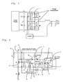
- the proposed current detection method according to the invention is implemented locally around each controlled switching device (MOSFET).
- the current limit is set by a predetermined reference that corresponds to the application and to the applied switching device.
- the current limiting is implemented as a self-oscillating circuit, provided locally around the switching device.
- the power stage is independent of all other control loops and acts only according to the current limit setting.
- the current limiting detection is done directly across the switching device by sensing the voltage drop across the device by an arrangement of diodes, current-sources and additional circuitry to measure and detect the voltage.
- the self-oscillating current limiting loop is implemented by assuring a fixed transistor off time.
- the current limit is detected by using a comparator circuit After a detection of an over-current situation, the output of the comparator changes to a new state which is held for a predetermined time period, e.g. 1.25 microseconds.
- the transistor driver circuit turns off the switching device according to the output state of the comparator circuit.
- the current limiting and sensing scheme does not need to communicate with the global control system.
- the means to measure and detect the current is integrated with the driver stage and the current limit control into the same chip (IC - Integrated Circuit).
- the current limiting scheme and method provide a self-oscillating controlled current limiting mode.
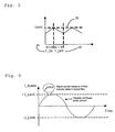
- the driver 16 to the output switching stage 17 is forced to turn OFF the output stage. If the over-current is detected, the control circuitry according to the invention will force a predetermined OFF time. This OFF time could be implemented in the comparator 6 used in the detection circuit. After the forced shutdown, the output stage is able to turn ON again according to the PWM signal 13 to the driver stage. If the over-current situation is still present, the current in the switching device 17 will ramp up to the current limit 22 and the output stage will be turned OFF again for the duration of the forced OFF time 23. Thereby, the output stage will enter the self-oscillating controlled current limiting mode with a switching frequency given by (T_ON(24) + T_OFF(23)) -1 .
- the self-oscillating controlled current limiting mode results in a self-oscillating current loop that cycle-by-cycle limits the current level and keeps the audio output intact but clipped. During this current-limit action, the amplifier control-loops will be saturated, which in the prior art stopped all switching action and caused unwanted audio artefacts.
- the current detection method according to the invention eliminates the need for an external sense device. Instead, the voltage across the FET transistor is used as a measure of the current through it.
- the FET transistors are either fully turned ON or fully turned OFF, and ON characteristics arc predominantly resistive.
- the invention takes advantage of this resistive nature of the FET transistors when turned ON and can by means of the invention sense the voltage across the MOSFET and thereby the current.
- the invention presents a new-to-the-art way of sensing the voltage across the switching device by using a special network and a sense current (3+10) to give information about the voltage across the device and thereby the current flowing through it.
- the sense current is divided into two equal parts taking two different paths.
- the first path goes through a diode 20 connected to the switching device 17, and the second path goes through a similar diode 4 to a capacitor 8. Since the two diodes are essentially equal, the voltage across the capacitor 8 will track the voltage across the switching device.
- the sense-current is bypassed by a switch 11 to avoid wrongful charging of the sense capacitor 8.
- the sense voltage across capacitor 8 is the input to a comparator 6.
- the input to the positive terminal of the comparator 6 is a voltage-reference 7.
- This voltage reference 7 can be a fixed voltage or an adjustable voltage. By implementing an adjustable voltage reference, the current limit level can be changed by adjusting the voltage 7.
- Another way of controlling the current limit setting is by adding a resistor 21 in series with the diode D1 20. Instead of having the detection voltage drop solely across the switching device, part of the drop will now be across the resistor 21. This will effectively reduce the current limit setting.
- the output of the comparator will change state which indicates an oven-current situation.
- the comparator output state 6 will force the driver stage 16 to shut down the switching device.
- the comparator will have a built-in forced hold time, e.g. 1.25 microseconds, in case of an over-current situation. After the forced hold time, the switching device can be turned ON again. If the over-current situation is still present, the switching device is turned OFF again for the duration of the forced hold time. By doing this, the current protection scheme transform the output stage to a self-oscillating controlled current limiting loop.
Landscapes
- Engineering & Computer Science (AREA)
- Power Engineering (AREA)
- Amplifiers (AREA)
- Tone Control, Compression And Expansion, Limiting Amplitude (AREA)
Claims (11)
- Verfahren zur Strommessung und Strombegrenzung in einem selbstoszillierenden Klasse D Verstärker, welcher einen Pulsweitenmodulator, eine Treiberschaltung, einen oder mehrere Leistungsschalthalbleiter (17) und ein globales Steuerungssystem umfasst, welches Verfahren folgendes umfasst:(i) Strommessung direkt an den Anschlusspunkten des besagten Leistungsschalthalbleiters (17), und(ii) Strombegrenzung mit Hilfe einer lokalen, autonom gesteuerten, selbstoszillierenden Schleife, die eine Komparatorschaltung mit Eingängen und Ausgängen umfasst, einen Bezugspegel und einen Detektionspegel für den besagten Komparator, der die besagte Treiberschaltung steuert,wo das besagte Verfahren durch eine Anordnung von Stromquellen, (3, 10), Dioden (4, 20) und Detektionsschaltkreisen gekennzeichnet ist zur Schaffung eines in zwei einander entsprechende Stromwege aufgeteilten Stromweg, wovon der erste Stromweg die Spannung an der Schalteinrichtung detektiert, und die Spannung an dem zweiten Stromweg folglich die hierdurch detektierte Spannung widerspiegelt und der Spannung an der Schalteinrichtung entspricht
- Verfahren zur Strombegrenzung gemäss Anspruch 1, wo die strombegrenzende Aktivität dadurch gekennzeichnet ist, dass die besagte Treiberschaltung im Falle einer Überstromdetektion die besagten Leistungsschalthalbleiter abschaltet.
- Verfahren zur Strombegrenzung gemäss Anspruch 1 und 2, wo die strombegrenzende Aktivität durch eine festgelegte Ausfallzeit für die besagten Leistungsschalthalbleiter gekennzeichnet ist
- Verfahren zur Strombegrenzung gemäss Anspruch 1, 2 und 3, wo die strombegrenzende Aktivität durch eine asynchron bestimmte Abschaltzeit für die besagten Leistungsschalthalbleiter gekennzeichnet ist
- Verfahren zur Strombegrenzung gemäss Anspruch 1, 2 und 3, dadurch gekennzeichnet, dass der besagte Komparator den Zustand des Ausgangs entsprechend dem Bezugspegel und dem Detektionspegel ändert
- Verfahren zur Strombegrenzung gemäss Aspruch 1, dadurch gekennzeichnet, dass der besagte Komparator eine gezwungene Haltezeit hat.
- Verfahren zur Strommessung und -begrenzung gemäss Anspruch 1 bis 6, dadurch gekennzeichnet, dass die Messungs- und Begrenzungsaktivität keine Verbindung mit dem besagten globalen Steuerungssystem hat
- Verfahren zur Strommessung und -begrenzung gemäss Anspruch 1 bis 7, gekennzeichnet durch die Integration in einen Chip (IC, integrierte Schaltung).
- Selbst-oszillierender Klasse D Verstärker, welcher einen Pulsweitenmodulator, eine Treiberschaltung, einen oder mehrere Leistungsschalthalbleiter und ein globales Steuerungssystem umfasst, wo der besagte selbst-oszillierende Klasse D Verstärker folgendes umfasst:(i) Mittel zur Strommessung direkt an den Anschlusspunkten des besagten Leistungsschalthalbleiters,(ii) eine Anordnung von Stromquellen, Dioden und Detektionsschaltkreisen zur Schaffung eines in zwei einander entsprechende Stromwege aufgeteilten Stromwegs, wovon der erste Stromweg die Spannung an der Schalteinrichtung detektiert, und die Spannung an dem zweiten Stromweg folglich die hierdurch detektierte Spannung widerspiegelt und der Spannung an der Schalteinrichtung entspricht,(iii) eine lokale, autonom gesteuerte, selbst-oszillierende Schleife, die eine Komparatorschaltung mit Eingängen und Ausgängen umfasst, einen Bezugspegel und einen Detektionspegel für den besagten Komparator, der die besagte Treiberschaltung steuert,(iv) Mittel zur Strombegrenzung, wo die besagte Komparatorschaltung die besagte Treiberschaltung mit einer festgelegten Ausfallzeit asynchron steuert
- Selbst-oszillierender Klasse D Verstärker gemäss Anspruch 9, umfassend.
ein Strommessung- und begrenzungssystem, das keine Verbindung mit dem besagten globalen Steuerungssystem hat - Selbst-oszillierender Klasse D Verstärker gemäss Anspruch 10, umfassend.
ein in einen Chip (IC, integrierte Schaltung) integriertes Strommessungs- und begrenzungssystem
Applications Claiming Priority (2)
| Application Number | Priority Date | Filing Date | Title |
|---|---|---|---|
| DKPA200601680 | 2006-12-20 | ||
| PCT/IB2007/055247 WO2008075306A1 (en) | 2006-12-20 | 2007-12-20 | True current limiting (tcl) |
Publications (2)
| Publication Number | Publication Date |
|---|---|
| EP2092639A1 EP2092639A1 (de) | 2009-08-26 |
| EP2092639B1 true EP2092639B1 (de) | 2011-09-21 |
Family
ID=39323002
Family Applications (1)
| Application Number | Title | Priority Date | Filing Date |
|---|---|---|---|
| EP07859471A Not-in-force EP2092639B1 (de) | 2006-12-20 | 2007-12-20 | Wahre Strombegrenzung |
Country Status (6)
| Country | Link |
|---|---|
| US (1) | US7936216B2 (de) |
| EP (1) | EP2092639B1 (de) |
| CN (1) | CN101563842B (de) |
| AT (1) | ATE525804T1 (de) |
| ES (1) | ES2370867T3 (de) |
| WO (1) | WO2008075306A1 (de) |
Families Citing this family (3)
| Publication number | Priority date | Publication date | Assignee | Title |
|---|---|---|---|---|
| US10824986B2 (en) * | 2010-12-23 | 2020-11-03 | Bladelogic, Inc. | Auto-suggesting IT asset groups using clustering techniques |
| US9756185B1 (en) | 2014-11-10 | 2017-09-05 | Teton1, Llc | System for automated call analysis using context specific lexicon |
| DE102019210566B4 (de) | 2019-07-17 | 2022-03-17 | Conti Temic Microelectronic Gmbh | Vorrichtung und Verfahren zum Messen eines durch eine PWM-angesteuerte induktive Last fließenden Stromes |
Family Cites Families (6)
| Publication number | Priority date | Publication date | Assignee | Title |
|---|---|---|---|---|
| US4415863A (en) * | 1981-03-24 | 1983-11-15 | Pioneer Electronic Corporation | Pulse width modulation amplifier |
| US5973569A (en) * | 1998-02-25 | 1999-10-26 | National Semiconductor Corporation | Short-circuit protection and over-current modulation to maximize audio amplifier output power |
| US6108182A (en) * | 1998-10-30 | 2000-08-22 | Intersil Corporation | Overcurrent sensing circuit and self adjusting blanking |
| JP2002171140A (ja) * | 2000-12-01 | 2002-06-14 | Mitsubishi Electric Corp | オーディオ信号増幅出力回路 |
| US7595615B2 (en) * | 2005-04-05 | 2009-09-29 | Texas Instruments Incorporated | Systems and methods for providing over-current protection in a switching power supply |
| US7317355B2 (en) * | 2005-05-10 | 2008-01-08 | Texas Instruments Incorporated | Over-current detection for a power field-effect transistor (FET) |
-
2007
- 2007-12-20 WO PCT/IB2007/055247 patent/WO2008075306A1/en not_active Ceased
- 2007-12-20 CN CN200780047379XA patent/CN101563842B/zh not_active Expired - Fee Related
- 2007-12-20 US US12/519,472 patent/US7936216B2/en active Active
- 2007-12-20 AT AT07859471T patent/ATE525804T1/de not_active IP Right Cessation
- 2007-12-20 ES ES07859471T patent/ES2370867T3/es active Active
- 2007-12-20 EP EP07859471A patent/EP2092639B1/de not_active Not-in-force
Also Published As
| Publication number | Publication date |
|---|---|
| EP2092639A1 (de) | 2009-08-26 |
| WO2008075306A1 (en) | 2008-06-26 |
| CN101563842B (zh) | 2012-03-28 |
| CN101563842A (zh) | 2009-10-21 |
| US20100033247A1 (en) | 2010-02-11 |
| ATE525804T1 (de) | 2011-10-15 |
| US7936216B2 (en) | 2011-05-03 |
| ES2370867T3 (es) | 2011-12-23 |
Similar Documents
| Publication | Publication Date | Title |
|---|---|---|
| US7554399B1 (en) | Protection circuit and method for protecting switching power amplifier circuits during reset | |
| JP5135214B2 (ja) | ソフトスタート回路を備えた突入電流制御システムおよび方法 | |
| US9772639B2 (en) | Dynamic current-limit circuit | |
| US7570118B1 (en) | Thermal overload protection circuit and method for protecting switching power amplifier circuits | |
| Morrow et al. | A 20-W stereo class-D audio output power stage in 0.6-/spl mu/m BCDMOS technology | |
| US7106031B2 (en) | Electric power supply apparatus having input switching circuit | |
| CN112803901B (zh) | 一种基于自适应过流保护的功率放大器 | |
| US20090273874A1 (en) | Power switch circuit exhibiting over current and short circuit protection and method for limiting the output current thereof | |
| CN107834985B (zh) | D级放大电路、其控制方法、音频输出装置、电子设备 | |
| US20060091961A1 (en) | Overcurrent protection circuit with fast current limiting control | |
| US8749303B2 (en) | Over-current protection for a switch mode class D audio amplifier | |
| US8427804B2 (en) | Power amplifier | |
| TW201320517A (zh) | 保護開路和/或短路狀況下電源變換系統的系統和方法 | |
| US20120014025A1 (en) | Overcurrent protection circuit and semiconductor device | |
| US20080043391A1 (en) | Timer reset circuit for overcurrent protection of switching power amplifier | |
| US20160233666A1 (en) | Current limiter circuit system | |
| JP2005249519A (ja) | 電流検出回路、負荷駆動回路、及び記憶装置 | |
| CN112534668A (zh) | 升压转换器短路保护 | |
| EP2092639B1 (de) | Wahre Strombegrenzung | |
| JPH03256407A (ja) | 制御回路 | |
| US7477502B1 (en) | Method and system for providing fault protection in a power supply system | |
| JP2008141612A (ja) | 負荷駆動装置の故障検出装置および負荷駆動用ic | |
| JP4517579B2 (ja) | 電流制御回路 | |
| JP2004282959A (ja) | 電圧制御型駆動素子の駆動装置 | |
| US6624995B2 (en) | Semiconductor device and method of activating a protection circuit with a sampling pulse |
Legal Events
| Date | Code | Title | Description |
|---|---|---|---|
| PUAI | Public reference made under article 153(3) epc to a published international application that has entered the european phase |
Free format text: ORIGINAL CODE: 0009012 |
|
| 17P | Request for examination filed |
Effective date: 20090720 |
|
| AK | Designated contracting states |
Kind code of ref document: A1 Designated state(s): AT BE BG CH CY CZ DE DK EE ES FI FR GB GR HU IE IS IT LI LT LU LV MC MT NL PL PT RO SE SI SK TR |
|
| DAX | Request for extension of the european patent (deleted) | ||
| 17Q | First examination report despatched |
Effective date: 20101123 |
|
| GRAP | Despatch of communication of intention to grant a patent |
Free format text: ORIGINAL CODE: EPIDOSNIGR1 |
|
| RTI1 | Title (correction) |
Free format text: TRUE CURRENT LIMIT |
|
| GRAS | Grant fee paid |
Free format text: ORIGINAL CODE: EPIDOSNIGR3 |
|
| GRAA | (expected) grant |
Free format text: ORIGINAL CODE: 0009210 |
|
| AK | Designated contracting states |
Kind code of ref document: B1 Designated state(s): AT BE BG CH CY CZ DE DK EE ES FI FR GB GR HU IE IS IT LI LT LU LV MC MT NL PL PT RO SE SI SK TR |
|
| REG | Reference to a national code |
Ref country code: GB Ref legal event code: FG4D |
|
| REG | Reference to a national code |
Ref country code: CH Ref legal event code: EP |
|
| REG | Reference to a national code |
Ref country code: IE Ref legal event code: FG4D |
|
| REG | Reference to a national code |
Ref country code: DE Ref legal event code: R096 Ref document number: 602007017431 Country of ref document: DE Effective date: 20111117 |
|
| REG | Reference to a national code |
Ref country code: ES Ref legal event code: FG2A Ref document number: 2370867 Country of ref document: ES Kind code of ref document: T3 Effective date: 20111223 |
|
| REG | Reference to a national code |
Ref country code: NL Ref legal event code: VDEP Effective date: 20110921 |
|
| PG25 | Lapsed in a contracting state [announced via postgrant information from national office to epo] |
Ref country code: FI Free format text: LAPSE BECAUSE OF FAILURE TO SUBMIT A TRANSLATION OF THE DESCRIPTION OR TO PAY THE FEE WITHIN THE PRESCRIBED TIME-LIMIT Effective date: 20110921 Ref country code: SE Free format text: LAPSE BECAUSE OF FAILURE TO SUBMIT A TRANSLATION OF THE DESCRIPTION OR TO PAY THE FEE WITHIN THE PRESCRIBED TIME-LIMIT Effective date: 20110921 Ref country code: LT Free format text: LAPSE BECAUSE OF FAILURE TO SUBMIT A TRANSLATION OF THE DESCRIPTION OR TO PAY THE FEE WITHIN THE PRESCRIBED TIME-LIMIT Effective date: 20110921 |
|
| LTIE | Lt: invalidation of european patent or patent extension |
Effective date: 20110921 |
|
| PG25 | Lapsed in a contracting state [announced via postgrant information from national office to epo] |
Ref country code: SI Free format text: LAPSE BECAUSE OF FAILURE TO SUBMIT A TRANSLATION OF THE DESCRIPTION OR TO PAY THE FEE WITHIN THE PRESCRIBED TIME-LIMIT Effective date: 20110921 Ref country code: CY Free format text: LAPSE BECAUSE OF FAILURE TO SUBMIT A TRANSLATION OF THE DESCRIPTION OR TO PAY THE FEE WITHIN THE PRESCRIBED TIME-LIMIT Effective date: 20110921 Ref country code: AT Free format text: LAPSE BECAUSE OF FAILURE TO SUBMIT A TRANSLATION OF THE DESCRIPTION OR TO PAY THE FEE WITHIN THE PRESCRIBED TIME-LIMIT Effective date: 20110921 Ref country code: LV Free format text: LAPSE BECAUSE OF FAILURE TO SUBMIT A TRANSLATION OF THE DESCRIPTION OR TO PAY THE FEE WITHIN THE PRESCRIBED TIME-LIMIT Effective date: 20110921 Ref country code: GR Free format text: LAPSE BECAUSE OF FAILURE TO SUBMIT A TRANSLATION OF THE DESCRIPTION OR TO PAY THE FEE WITHIN THE PRESCRIBED TIME-LIMIT Effective date: 20111222 |
|
| REG | Reference to a national code |
Ref country code: AT Ref legal event code: MK05 Ref document number: 525804 Country of ref document: AT Kind code of ref document: T Effective date: 20110921 |
|
| PG25 | Lapsed in a contracting state [announced via postgrant information from national office to epo] |
Ref country code: BE Free format text: LAPSE BECAUSE OF FAILURE TO SUBMIT A TRANSLATION OF THE DESCRIPTION OR TO PAY THE FEE WITHIN THE PRESCRIBED TIME-LIMIT Effective date: 20110921 |
|
| PG25 | Lapsed in a contracting state [announced via postgrant information from national office to epo] |
Ref country code: IS Free format text: LAPSE BECAUSE OF FAILURE TO SUBMIT A TRANSLATION OF THE DESCRIPTION OR TO PAY THE FEE WITHIN THE PRESCRIBED TIME-LIMIT Effective date: 20120121 Ref country code: CZ Free format text: LAPSE BECAUSE OF FAILURE TO SUBMIT A TRANSLATION OF THE DESCRIPTION OR TO PAY THE FEE WITHIN THE PRESCRIBED TIME-LIMIT Effective date: 20110921 Ref country code: SK Free format text: LAPSE BECAUSE OF FAILURE TO SUBMIT A TRANSLATION OF THE DESCRIPTION OR TO PAY THE FEE WITHIN THE PRESCRIBED TIME-LIMIT Effective date: 20110921 |
|
| PG25 | Lapsed in a contracting state [announced via postgrant information from national office to epo] |
Ref country code: EE Free format text: LAPSE BECAUSE OF FAILURE TO SUBMIT A TRANSLATION OF THE DESCRIPTION OR TO PAY THE FEE WITHIN THE PRESCRIBED TIME-LIMIT Effective date: 20110921 Ref country code: PT Free format text: LAPSE BECAUSE OF FAILURE TO SUBMIT A TRANSLATION OF THE DESCRIPTION OR TO PAY THE FEE WITHIN THE PRESCRIBED TIME-LIMIT Effective date: 20120123 Ref country code: PL Free format text: LAPSE BECAUSE OF FAILURE TO SUBMIT A TRANSLATION OF THE DESCRIPTION OR TO PAY THE FEE WITHIN THE PRESCRIBED TIME-LIMIT Effective date: 20110921 Ref country code: NL Free format text: LAPSE BECAUSE OF FAILURE TO SUBMIT A TRANSLATION OF THE DESCRIPTION OR TO PAY THE FEE WITHIN THE PRESCRIBED TIME-LIMIT Effective date: 20110921 Ref country code: RO Free format text: LAPSE BECAUSE OF FAILURE TO SUBMIT A TRANSLATION OF THE DESCRIPTION OR TO PAY THE FEE WITHIN THE PRESCRIBED TIME-LIMIT Effective date: 20110921 |
|
| PLBE | No opposition filed within time limit |
Free format text: ORIGINAL CODE: 0009261 |
|
| STAA | Information on the status of an ep patent application or granted ep patent |
Free format text: STATUS: NO OPPOSITION FILED WITHIN TIME LIMIT |
|
| PG25 | Lapsed in a contracting state [announced via postgrant information from national office to epo] |
Ref country code: MC Free format text: LAPSE BECAUSE OF NON-PAYMENT OF DUE FEES Effective date: 20111231 Ref country code: DK Free format text: LAPSE BECAUSE OF FAILURE TO SUBMIT A TRANSLATION OF THE DESCRIPTION OR TO PAY THE FEE WITHIN THE PRESCRIBED TIME-LIMIT Effective date: 20110921 |
|
| REG | Reference to a national code |
Ref country code: CH Ref legal event code: PL |
|
| 26N | No opposition filed |
Effective date: 20120622 |
|
| REG | Reference to a national code |
Ref country code: IE Ref legal event code: MM4A |
|
| REG | Reference to a national code |
Ref country code: DE Ref legal event code: R097 Ref document number: 602007017431 Country of ref document: DE Effective date: 20120622 |
|
| PG25 | Lapsed in a contracting state [announced via postgrant information from national office to epo] |
Ref country code: IE Free format text: LAPSE BECAUSE OF NON-PAYMENT OF DUE FEES Effective date: 20111220 Ref country code: CH Free format text: LAPSE BECAUSE OF NON-PAYMENT OF DUE FEES Effective date: 20111231 Ref country code: LI Free format text: LAPSE BECAUSE OF NON-PAYMENT OF DUE FEES Effective date: 20111231 |
|
| PG25 | Lapsed in a contracting state [announced via postgrant information from national office to epo] |
Ref country code: MT Free format text: LAPSE BECAUSE OF FAILURE TO SUBMIT A TRANSLATION OF THE DESCRIPTION OR TO PAY THE FEE WITHIN THE PRESCRIBED TIME-LIMIT Effective date: 20110921 |
|
| PG25 | Lapsed in a contracting state [announced via postgrant information from national office to epo] |
Ref country code: LU Free format text: LAPSE BECAUSE OF NON-PAYMENT OF DUE FEES Effective date: 20111220 |
|
| PG25 | Lapsed in a contracting state [announced via postgrant information from national office to epo] |
Ref country code: BG Free format text: LAPSE BECAUSE OF FAILURE TO SUBMIT A TRANSLATION OF THE DESCRIPTION OR TO PAY THE FEE WITHIN THE PRESCRIBED TIME-LIMIT Effective date: 20111221 |
|
| PG25 | Lapsed in a contracting state [announced via postgrant information from national office to epo] |
Ref country code: TR Free format text: LAPSE BECAUSE OF FAILURE TO SUBMIT A TRANSLATION OF THE DESCRIPTION OR TO PAY THE FEE WITHIN THE PRESCRIBED TIME-LIMIT Effective date: 20110921 |
|
| PG25 | Lapsed in a contracting state [announced via postgrant information from national office to epo] |
Ref country code: HU Free format text: LAPSE BECAUSE OF FAILURE TO SUBMIT A TRANSLATION OF THE DESCRIPTION OR TO PAY THE FEE WITHIN THE PRESCRIBED TIME-LIMIT Effective date: 20110921 |
|
| PGFP | Annual fee paid to national office [announced via postgrant information from national office to epo] |
Ref country code: ES Payment date: 20141215 Year of fee payment: 8 Ref country code: GB Payment date: 20141205 Year of fee payment: 8 |
|
| PGFP | Annual fee paid to national office [announced via postgrant information from national office to epo] |
Ref country code: IT Payment date: 20141216 Year of fee payment: 8 |
|
| PGFP | Annual fee paid to national office [announced via postgrant information from national office to epo] |
Ref country code: DE Payment date: 20141203 Year of fee payment: 8 |
|
| PGFP | Annual fee paid to national office [announced via postgrant information from national office to epo] |
Ref country code: FR Payment date: 20141212 Year of fee payment: 8 |
|
| REG | Reference to a national code |
Ref country code: DE Ref legal event code: R119 Ref document number: 602007017431 Country of ref document: DE |
|
| GBPC | Gb: european patent ceased through non-payment of renewal fee |
Effective date: 20151220 |
|
| REG | Reference to a national code |
Ref country code: FR Ref legal event code: ST Effective date: 20160831 |
|
| PG25 | Lapsed in a contracting state [announced via postgrant information from national office to epo] |
Ref country code: GB Free format text: LAPSE BECAUSE OF NON-PAYMENT OF DUE FEES Effective date: 20151220 Ref country code: DE Free format text: LAPSE BECAUSE OF NON-PAYMENT OF DUE FEES Effective date: 20160701 |
|
| PG25 | Lapsed in a contracting state [announced via postgrant information from national office to epo] |
Ref country code: FR Free format text: LAPSE BECAUSE OF NON-PAYMENT OF DUE FEES Effective date: 20151231 |
|
| PG25 | Lapsed in a contracting state [announced via postgrant information from national office to epo] |
Ref country code: IT Free format text: LAPSE BECAUSE OF NON-PAYMENT OF DUE FEES Effective date: 20151220 |
|
| PG25 | Lapsed in a contracting state [announced via postgrant information from national office to epo] |
Ref country code: ES Free format text: LAPSE BECAUSE OF NON-PAYMENT OF DUE FEES Effective date: 20151221 |
|
| REG | Reference to a national code |
Ref country code: ES Ref legal event code: FD2A Effective date: 20180710 |