EP2092810B1 - Installation de fabrication d'une carte de circuits imprimés dotée d'éléments de câblage en cuivre additionnels intégrés et mis en contact par ultrasons - Google Patents
Installation de fabrication d'une carte de circuits imprimés dotée d'éléments de câblage en cuivre additionnels intégrés et mis en contact par ultrasons Download PDFInfo
- Publication number
- EP2092810B1 EP2092810B1 EP20070846548 EP07846548A EP2092810B1 EP 2092810 B1 EP2092810 B1 EP 2092810B1 EP 20070846548 EP20070846548 EP 20070846548 EP 07846548 A EP07846548 A EP 07846548A EP 2092810 B1 EP2092810 B1 EP 2092810B1
- Authority
- EP
- European Patent Office
- Prior art keywords
- circuit board
- installation
- producing
- sonotrode
- board according
- Prior art date
- Legal status (The legal status is an assumption and is not a legal conclusion. Google has not performed a legal analysis and makes no representation as to the accuracy of the status listed.)
- Active
Links
Images



Classifications
-
- B—PERFORMING OPERATIONS; TRANSPORTING
- B23—MACHINE TOOLS; METAL-WORKING NOT OTHERWISE PROVIDED FOR
- B23K—SOLDERING OR UNSOLDERING; WELDING; CLADDING OR PLATING BY SOLDERING OR WELDING; CUTTING BY APPLYING HEAT LOCALLY, e.g. FLAME CUTTING; WORKING BY LASER BEAM
- B23K20/00—Non-electric welding by applying impact or other pressure, with or without the application of heat, e.g. cladding or plating
- B23K20/002—Non-electric welding by applying impact or other pressure, with or without the application of heat, e.g. cladding or plating specially adapted for particular articles or work
- B23K20/004—Wire welding
-
- H—ELECTRICITY
- H05—ELECTRIC TECHNIQUES NOT OTHERWISE PROVIDED FOR
- H05K—PRINTED CIRCUITS; CASINGS OR CONSTRUCTIONAL DETAILS OF ELECTRIC APPARATUS; MANUFACTURE OF ASSEMBLAGES OF ELECTRICAL COMPONENTS
- H05K3/00—Apparatus or processes for manufacturing printed circuits
- H05K3/10—Apparatus or processes for manufacturing printed circuits in which conductive material is applied to the insulating support in such a manner as to form the desired conductive pattern
- H05K3/103—Apparatus or processes for manufacturing printed circuits in which conductive material is applied to the insulating support in such a manner as to form the desired conductive pattern by bonding or embedding conductive wires or strips
-
- H—ELECTRICITY
- H05—ELECTRIC TECHNIQUES NOT OTHERWISE PROVIDED FOR
- H05K—PRINTED CIRCUITS; CASINGS OR CONSTRUCTIONAL DETAILS OF ELECTRIC APPARATUS; MANUFACTURE OF ASSEMBLAGES OF ELECTRICAL COMPONENTS
- H05K3/00—Apparatus or processes for manufacturing printed circuits
- H05K3/22—Secondary treatment of printed circuits
- H05K3/222—Completing of printed circuits by adding non-printed jumper connections
-
- H—ELECTRICITY
- H05—ELECTRIC TECHNIQUES NOT OTHERWISE PROVIDED FOR
- H05K—PRINTED CIRCUITS; CASINGS OR CONSTRUCTIONAL DETAILS OF ELECTRIC APPARATUS; MANUFACTURE OF ASSEMBLAGES OF ELECTRICAL COMPONENTS
- H05K3/00—Apparatus or processes for manufacturing printed circuits
- H05K3/30—Assembling printed circuits with electric components, e.g. with resistors
- H05K3/32—Assembling printed circuits with electric components, e.g. with resistors electrically connecting electric components or wires to printed circuits
- H05K3/328—Assembling printed circuits with electric components, e.g. with resistors electrically connecting electric components or wires to printed circuits by welding
-
- B—PERFORMING OPERATIONS; TRANSPORTING
- B23—MACHINE TOOLS; METAL-WORKING NOT OTHERWISE PROVIDED FOR
- B23K—SOLDERING OR UNSOLDERING; WELDING; CLADDING OR PLATING BY SOLDERING OR WELDING; CUTTING BY APPLYING HEAT LOCALLY, e.g. FLAME CUTTING; WORKING BY LASER BEAM
- B23K2101/00—Articles made by soldering, welding or cutting
- B23K2101/36—Electric or electronic devices
- B23K2101/42—Printed circuits
-
- H—ELECTRICITY
- H05—ELECTRIC TECHNIQUES NOT OTHERWISE PROVIDED FOR
- H05K—PRINTED CIRCUITS; CASINGS OR CONSTRUCTIONAL DETAILS OF ELECTRIC APPARATUS; MANUFACTURE OF ASSEMBLAGES OF ELECTRICAL COMPONENTS
- H05K2201/00—Indexing scheme relating to printed circuits covered by H05K1/00
- H05K2201/03—Conductive materials
- H05K2201/0332—Structure of the conductor
- H05K2201/0335—Layered conductors or foils
- H05K2201/0355—Metal foils
-
- H—ELECTRICITY
- H05—ELECTRIC TECHNIQUES NOT OTHERWISE PROVIDED FOR
- H05K—PRINTED CIRCUITS; CASINGS OR CONSTRUCTIONAL DETAILS OF ELECTRIC APPARATUS; MANUFACTURE OF ASSEMBLAGES OF ELECTRICAL COMPONENTS
- H05K2201/00—Indexing scheme relating to printed circuits covered by H05K1/00
- H05K2201/10—Details of components or other objects attached to or integrated in a printed circuit board
- H05K2201/10227—Other objects, e.g. metallic pieces
- H05K2201/1028—Thin metal strips as connectors or conductors
-
- H—ELECTRICITY
- H05—ELECTRIC TECHNIQUES NOT OTHERWISE PROVIDED FOR
- H05K—PRINTED CIRCUITS; CASINGS OR CONSTRUCTIONAL DETAILS OF ELECTRIC APPARATUS; MANUFACTURE OF ASSEMBLAGES OF ELECTRICAL COMPONENTS
- H05K2201/00—Indexing scheme relating to printed circuits covered by H05K1/00
- H05K2201/10—Details of components or other objects attached to or integrated in a printed circuit board
- H05K2201/10227—Other objects, e.g. metallic pieces
- H05K2201/10287—Metal wires as connectors or conductors
-
- H—ELECTRICITY
- H05—ELECTRIC TECHNIQUES NOT OTHERWISE PROVIDED FOR
- H05K—PRINTED CIRCUITS; CASINGS OR CONSTRUCTIONAL DETAILS OF ELECTRIC APPARATUS; MANUFACTURE OF ASSEMBLAGES OF ELECTRICAL COMPONENTS
- H05K2203/00—Indexing scheme relating to apparatus or processes for manufacturing printed circuits covered by H05K3/00
- H05K2203/02—Details related to mechanical or acoustic processing, e.g. drilling, punching, cutting, using ultrasound
- H05K2203/0285—Using ultrasound, e.g. for cleaning, soldering or wet treatment
-
- H—ELECTRICITY
- H10—SEMICONDUCTOR DEVICES; ELECTRIC SOLID-STATE DEVICES NOT OTHERWISE PROVIDED FOR
- H10W—GENERIC PACKAGES, INTERCONNECTIONS, CONNECTORS OR OTHER CONSTRUCTIONAL DETAILS OF DEVICES COVERED BY CLASS H10
- H10W72/00—Interconnections or connectors in packages
- H10W72/071—Connecting or disconnecting
- H10W72/0711—Apparatus therefor
- H10W72/07141—Means for applying energy, e.g. ovens or lasers
-
- H—ELECTRICITY
- H10—SEMICONDUCTOR DEVICES; ELECTRIC SOLID-STATE DEVICES NOT OTHERWISE PROVIDED FOR
- H10W—GENERIC PACKAGES, INTERCONNECTIONS, CONNECTORS OR OTHER CONSTRUCTIONAL DETAILS OF DEVICES COVERED BY CLASS H10
- H10W72/00—Interconnections or connectors in packages
- H10W72/071—Connecting or disconnecting
- H10W72/0711—Apparatus therefor
- H10W72/07163—Means for mechanical processing, e.g. for planarising, pressing, stamping or drilling
-
- H—ELECTRICITY
- H10—SEMICONDUCTOR DEVICES; ELECTRIC SOLID-STATE DEVICES NOT OTHERWISE PROVIDED FOR
- H10W—GENERIC PACKAGES, INTERCONNECTIONS, CONNECTORS OR OTHER CONSTRUCTIONAL DETAILS OF DEVICES COVERED BY CLASS H10
- H10W72/00—Interconnections or connectors in packages
- H10W72/071—Connecting or disconnecting
- H10W72/0711—Apparatus therefor
- H10W72/07168—Means for storing or moving the material for the connector
-
- H—ELECTRICITY
- H10—SEMICONDUCTOR DEVICES; ELECTRIC SOLID-STATE DEVICES NOT OTHERWISE PROVIDED FOR
- H10W—GENERIC PACKAGES, INTERCONNECTIONS, CONNECTORS OR OTHER CONSTRUCTIONAL DETAILS OF DEVICES COVERED BY CLASS H10
- H10W72/00—Interconnections or connectors in packages
- H10W72/071—Connecting or disconnecting
- H10W72/0711—Apparatus therefor
- H10W72/07178—Means for aligning
-
- H—ELECTRICITY
- H10—SEMICONDUCTOR DEVICES; ELECTRIC SOLID-STATE DEVICES NOT OTHERWISE PROVIDED FOR
- H10W—GENERIC PACKAGES, INTERCONNECTIONS, CONNECTORS OR OTHER CONSTRUCTIONAL DETAILS OF DEVICES COVERED BY CLASS H10
- H10W72/00—Interconnections or connectors in packages
- H10W72/071—Connecting or disconnecting
- H10W72/075—Connecting or disconnecting of bond wires
- H10W72/07502—Connecting or disconnecting of bond wires using an auxiliary member
-
- H—ELECTRICITY
- H10—SEMICONDUCTOR DEVICES; ELECTRIC SOLID-STATE DEVICES NOT OTHERWISE PROVIDED FOR
- H10W—GENERIC PACKAGES, INTERCONNECTIONS, CONNECTORS OR OTHER CONSTRUCTIONAL DETAILS OF DEVICES COVERED BY CLASS H10
- H10W72/00—Interconnections or connectors in packages
- H10W72/071—Connecting or disconnecting
- H10W72/075—Connecting or disconnecting of bond wires
- H10W72/07531—Techniques
- H10W72/07532—Compression bonding, e.g. thermocompression bonding
- H10W72/07533—Ultrasonic bonding, e.g. thermosonic bonding
-
- H—ELECTRICITY
- H10—SEMICONDUCTOR DEVICES; ELECTRIC SOLID-STATE DEVICES NOT OTHERWISE PROVIDED FOR
- H10W—GENERIC PACKAGES, INTERCONNECTIONS, CONNECTORS OR OTHER CONSTRUCTIONAL DETAILS OF DEVICES COVERED BY CLASS H10
- H10W72/00—Interconnections or connectors in packages
- H10W72/50—Bond wires
- H10W72/531—Shapes of wire connectors
- H10W72/5363—Shapes of wire connectors the connected ends being wedge-shaped
-
- H—ELECTRICITY
- H10—SEMICONDUCTOR DEVICES; ELECTRIC SOLID-STATE DEVICES NOT OTHERWISE PROVIDED FOR
- H10W—GENERIC PACKAGES, INTERCONNECTIONS, CONNECTORS OR OTHER CONSTRUCTIONAL DETAILS OF DEVICES COVERED BY CLASS H10
- H10W72/00—Interconnections or connectors in packages
- H10W72/50—Bond wires
- H10W72/551—Materials of bond wires
- H10W72/552—Materials of bond wires comprising metals or metalloids, e.g. silver
- H10W72/5525—Materials of bond wires comprising metals or metalloids, e.g. silver comprising copper [Cu]
Definitions
- the invention relates to a system for producing a printed circuit board having at least one additional electrically conductive structure in the form of a round or rectangular electrically conductive wiring element, in particular in the form of an elongated Kupferatory copper-containing element, which is contacted as an additive element at least partially flat on copper foil elements by means of ultrasound and is integrated in a further printed circuit board manufacturing process by means of lamination in a printed circuit board.
- WO02067642A1 or the DE10108168C1 is a method for producing a multi-wire circuit board, in which defined on one side of a thin sheet of electrically conductive material by means of spaced adhesive bonding leads laid and at predetermined contact points of the sheet electrically by means of welding, bonding, soldering, conductive adhesives or the like. be contacted.
- a mechanical stabilizing element in the form of a prepreg or in the form of an electrically conductive or insulating surface element applied by means of insulating film is provided on the fixed conductor wires.
- the surface element is thereby structured from the other side in such a way that the contact points are separated from the remaining surface element.
- Lead wires are routed defined by adhesive surfaces.
- the lead wires which are profiled on their own, are electrically conductively connected to the remaining parts of the printed circuit board by means of a weld or a bonding connection.
- a relatively thinner and round wire cross section on a large-scale, metallized copper plate can be contacted only pointwise.
- a method for welding a conductor wire with a conductive foil which is preferably intended for connection to a printed circuit board carrier for producing a printed circuit board, wherein the thickness or the diameter of the conductor wire is preferably greater than the thickness of the conductive foil and wherein the conductive foil is in contact at least during the welding with a thermal separating plate whose thermal conductivity is lower than that of the conductive film.
- a separating plate in an ultrasonic welding on an already etched inner layer with an epoxy-glass fabric structure on the back cause no good thermal dissipation, since such a structure conducts very poor thermal.
- the publication JP 57-91533 discloses a system for producing a printed circuit board, which describes a device for the separation of a wire element. However, the system does not show an ultrasonic sonotrode head with a hold-down device.
- the object of the present invention is therefore to provide a system for the cost-effective production of multifunctional printed circuit boards for the wiring of highly complex conductor structures, in particular fine to Feinstleiter Modellen, together with structures for conducting relatively high currents on a circuit board.
- a system consisting of a table and a horizontally arranged sonotrode head with ultrasonic generator and a feed system including hold-down system and a tear-off system for the wiring element will be described.
- the sonotrode head with ultrasonic generator is arranged vertically and with a torsional vibration system, larger-area intermetallic compounds are welded by means of ultrasonic energy.
- Both embodiments can be integrated into one system or can be implemented separately or else sequentially in a multiple system and in both systems only the sonotrode head or only the sonotrode head can be used
- Table can be moved in x and y direction or the sonotrode head in one direction and the table can be moved in the other direction.
- the table top is replaceable and can be so quickly cleaned by the pressure during the ultrasonic contacting such Abnweilept.
- the sonotrode tools are changeable and a fully automatic tool changer can be used.
- the shapes of the sonotrodes are thereby formed triangular or trapezoidal and thus round or rectangular wiring elements in the ultrasonic connections are deformed so that the contact surfaces of the wiring to the copper foil surface is significantly larger than the contact surface without a sonotrode shape formed in this way. By enlarging the contact surface, a much better current distribution and thermal coupling to the copper foil is achieved.
- At least one elongated wiring element is deformed in cross-section by means of a specially shaped sonotrode in the at least partially flat contact region in such a way that the contact surface is increased by preferably 20% relative to the underlying film. Further preferred embodiments even provide for an increase of the contact area by more than 30% and more particularly by more than 50% compared to an undeformed (linear) contact surface (of a round wire).
- the wiring element is deformed approximately triangular-like or trapezoidal in cross-section. As a result, the desired enlargement of the contact surface is achieved.
- triangular or trapezoidal deformations are provided, with the aim to set up the blunt (and almost flattened) side of the wiring element with a larger surface area on the flat film and to weld there.
- the heat transfers are distributed over a larger area and there is no risk of damage to the sensitive film. If a resistance welding is used, then even the welding current can be increased without the risk that the sensitive CU film is damaged.
- the wiring elements are to receive a flattened shape with a matched sonotrode only at the location of their welding on the copper foil.
- a sonotrode that makes a flattened shape at the site of welding a round wire has one triangular cross-section with a length of about 2 - 3 mm.
- the depth of the V-shaped recess in the sonotrode must be smaller than the diameter of the received therein cross section of the triangularly deformed wire.
- Such a round wire has, for example, a diameter of 500 .mu.m. This avoids that the sonotrode itself rests on the CU foil, which would otherwise damage them.
- the sonotrode must ensure a large area on the CU surface of the wire to be deformed, otherwise the friction welding energy could not be transmitted sufficiently. Due to the pressure of the sonotrode on the round cross-section of the copper conductor (wiring element) and the US energy, the cross-section is flattened and pressed with its flattened broadside on the surface of the CU film and welded there by friction welding materially. Thus, a much larger contact surface is achieved in the coupling to the underlying CU film.
- This CU film has a thickness of only 9 or 17 or 35 microns. This information relates to standardized thicknesses of commonly used CU films.
- the deformation of a round wire in a (flattened) triangular profile at the location of its welding on the CU film refers only to a preferred embodiment of the invention.
- the invention includes all flattened profile shapes of such round wires. In particular, right or square profiles or oval, trapezoidal and parallelogram profile shapes.
- the wiring elements are preferably supplied controlled by a roller NC, but can also be supplied in principle as a prefabricated element from a magazine piece by piece.
- the film area to which a wiring element is to be applied surface by piece pre-cleaned by means of a cleaning sonotrode of titanium and thereby the thin oxide layer, which forms on non-passivated copper surfaces within a few hours, eliminated and so can a subsequent ultrasonic bonding process a good surface ultrasonic connection can be achieved.
- the band-shaped wiring elements are contacted repeatedly and at predetermined intervals by means of ultrasound on the underneath copper foil during the laying process and it can thereby be an angling of, for example, 45 ° and below and realized. Consequently, the wiring elements can not only be laid in a line, but with correspondingly predetermined geometries.
- the residence time of the sonotrode after the ultrasonic welding process is an essential criterion in such laying processes.
- Such US sonotrodes have a greater mass than the laying wire element and the underlying copper foil and have a good thermal dissipation and, moreover, can be formed so that a passive or active increased heat dissipation is established. In this way, it is possible to prevent the sonotrode from being heated too much, even with a large number of ultrasound welds which are separated by a short time, so that the sonotrode can dissipate any heat development in the welding partners.
- the residence time is also advantageous for the tear-off process or a bending process, as it does the weld is additionally stabilized by a corresponding contact pressure.
- the invention accordingly also relates to a printed circuit board with additional functional elements.
- a highly complex fine structure on a printed circuit board with the possibility of wiring high-current-carrying components is described on a circuit board.
- electrically conductive wiring elements are preferably surface-mounted by means of friction welding or ultrasonic welding on an etched conductor structure produced thereunder and subsequently machined by means of appropriate resin systems.
- electrically conductive wiring elements are fastened by means of friction welding or ultrasound in an insulating manner on a printed circuit board substrate.
- the insulating layer may be arranged over the entire surface or selectively on the corresponding circuit board surface, or the electrically conductive wiring element may be provided on the corresponding side or enveloping with a corresponding resin. This way becomes a stand-alone Wiring level produced.
- the subsequent leveling by means of suitable resin systems can be carried out as in the first embodiment.
- flat wiring elements are used as selective heat-dissipating elements.
- planar elements are positioned in an inner layer or on one of the two surfaces and it is made after the leveling or lamination an opening such that the respective component can be mounted in direct heat-conductive contact.
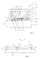
- FIG. 1 is a schematic representation of a system (1) for producing a printed circuit board (2) with at least one additional electrically conductive structure (4) in the form of a round or rectangular electrically conductive wiring element (4) using a horizontally arranged ultrasonic sonotrode system (5) the welding of smaller wiring element (4) cross sections shown.
- a multifunctional printed circuit board (2) is positioned in the unfinished state or a substrate (3) with a full-surface or already structured copper foil (20) on a table (15) or positioned and held with a clamping or registration system (14).
- a vacuum suction table may be used or an auxiliary carrier may be used.
- the table (15) is based on the sonotrode ultrasound system (5) in the xyz direction NC-controlled movable, wherein in a first embodiment, the table for the input and output of the circuit board (2) or the substrate (3) the copper foil (20) is used and the entire upper work consisting of the sonotrode system (5), the hold-down (13), the notching system (12), the clamping system (11), the guide (10), the first and second eyelet (8, 9) and the coil (7) is designed to be movable and in addition, a part thereof is rotatable by 360 ° and in such angled laying a wiring element (4) is possible.
- the coil (7) is shown vertically arranged, but it can just as well horizontal as in FIG. 3 be arranged.
- the eyelets (8, 9) are used to compensate for the different winding diameter of a coil (7) with, for example, 100 m wiring element (4) and just introduce this into the guide element (10).
- the clamping system (11) is shown in this illustration with jaws from above and below, however, is performed optimally depending on the wiring element cross-section used (4) and can be carried out laterally or repeatedly.
- the clamping system (11) is designed such that the wiring element (4) is designed to act at an angle of a few degrees up to about 20 ° upwards.
- the tearing process by means of notching system (12) is easier and better.
- the notching system (12) does not score or cut through the wiring element (4) completely, since, due to tolerances, an anchoring of the printed circuit board (20) underneath can not be avoided.
- the notching system (12) will therefore, with a certain safety distance from the copper surface (20), perform the wiring element (4) with at least one notch greater than half the height of the wiring element (4).
- the sonotrode (5) clamps the wiring element (4) in the area of the planar one Ultrasonic contact point (21) with on the table (15) or against the table (15).
- the free end of the segment is first lifted off the surface of the copper foil and the partial kerf cut is carried out in the part of the segment which is still resting on the surface of the copper foil. Thereafter, the partially notched and lifted off the surface of the copper foil end is torn off.
- the distances, in contrast to this schematic representation, between the end of the guide (10), the clamping system (11), the notching system (12), the sonotrode tool (5) and the hold-down (13) are very small or closely spaced, so that an exact and NC-controlled positioning of a cut-to-length wiring element (4) on the surface of a copper foil element (20) and their surface welding is possible.
- the ultrasonic welding takes place when using round wire elements (4) with corresponding triangular or trapezoidal sonotrodes, so that the contact area (21) is substantially larger compared to the linear contact of a round wire element (4) on a plangeraden copper surface (20).
- FIG. 2 is a schematic representation of a system (1) for producing a printed circuit board (2) with at least one additional electrically conductive structure (4) in the form of a round or rectangular electrically conductive wiring element (4) using a vertically arranged ultrasonic sonotrode system (6)
- flat wire elements (4) with a cross section of a few millimeters to about 10 mm and typically 2 to 5 mm wide at a thickness of several 100 microns, typically in the range of about 200 to 500 microns, laid.
- a torsional vibration ultrasound system (6) has proven itself.
- the corresponding sonotrodes (6) are provided with a corresponding surface structure, so that a good ultrasonic friction welding energy input is possible and the surface of the wiring element (4) has only small impressions or notches. Moreover, even with a flat-shaped wiring element (4), the sonotrode (6) can be made trapezoidal. Thus, the lateral portions of the wiring member (4) are chamfered, and in a circuit board lamination method, a better resin embedding is performed.
- FIG. 3 is a schematic representation of a system (1) for producing a printed circuit board (2) with at least one additional electrically conductive structure (4) in the form of a round or rectangular electrically conductive wiring element (4), wherein in this illustration a Ultrasonic sonotrode-notched coil unit (16) is shown summarized and this unit (16) rotatable by up to 360 ° is executed and in such angled installation of a wiring element (4) is possible.
- the sonotrode system (5, 6) including hold-down device (13) can also be made rotatable or selectively rotatable, and the other elements NC controlled are rotated in accordance with the desired bending of the wiring element (13).
- FIG. 4 a schematic representation of the notch tear-off principle is shown.
- a notched cutting edge (12) NC is lowered controlled and notches the wire element (4) with the height (17) to a notch (18).
- the notch depth (18) With the notch depth (18), the remaining non-notched height of the wire element (4) is understood, which is torn off by means of clamping system (11).
- the notch depth (18) is dimensioned such that secured no notching or touching the surface of the copper foil (20) takes place.
- the notch will amount to at least 50% of the height (17) of a wiring element (4) and is achieved according to the invention by the Anwinkelung (19) of the clamping system (11) and the notch effect a lower tearing force. If only a residual cross section of 25% were not scored and tried to tear off the straight, not lifted off from the surface end of the wiring element, the copper foil 20 would deform. This is avoided with the lifting of the free end by the lifting angle 19. The necessary tearing force is lower and deformation of the copper foil 20 is avoided.
- FIG. 5 is a plan view of a pattern plate (25) made of full-surface and non-etched 70 micron thick copper foil (20) with piecewise ultrasonically welded (21) 500 microns copper wires (4) shown.
- Sample board (25) was executed in a variety of variants.
- the photograph shows the contacting of 500 ⁇ m thick copper round wire (4) on a 70 ⁇ m thick copper foil (20), which is not structured and has no resin carrier.
- Such a copper foil (20) is subjected to a lamination process after the application of the wire elements (4) and / or etched on the opposite side of the wire elements (4) or the wire elements (4) in the laminating process in a printed circuit board press according to the prior art in the resin layer embedded.
- FIG. 5 are single round wire elements (4) contacted by ultrasound at different distances to the copper foil (20). These attempts per wire cross-section are used to optimize the sonotrode or the holddown of the wire elements (4) for a plane as possible laying, that is, the wire elements (4) between the individual ultrasonic ultrasonic pads (21) arranged in line contact on the copper surface (4) become.
- FIG. 5 the angled installation shown.
- the sonotrode head (5, 6) including the wire feed is rotated by 45 °, for example, or else the table with the copper foil (20) is rotated.
- the wire (4) must be bent. It must therefore be mechanically held down during the ultrasonic welding process until the bending process is completed.
- an ultrasonic welding process is a largely cold welding process, in the area of the formation of the intermetallic compound, a relatively high temperature up to the melting point of copper at 1083 ° C is achieved.
- a sonotrode (5, 6) usually has a relatively large mass in comparison to the wire elements (4), the residence time of the sonotrode (5, 6) after the ultrasonic welding process can cause the dissipation of the heat generated and, moreover, a mechanical solidification by the Effect pressurization.
- the US sonotrode (5, 6) can also be provided with an active cooling.
- FIG. 6 is a cutout (26) from the top view of the pattern board (25) FIG. 5 with a detailed view of the two-dimensional ultrasonic contact points (21) including the tear-off ends (24) of the wiring elements (4) and the bends (23) shown.
- FIG. 7 schematically shows a section through a substrate (3) with a conductor track (4) with a round wire (2) and a sonotrode arranged above it (26) prior to contacting.
- the sonotrode (26) touches the wire (2) only at certain points, that is to say just at the moment from which a deformation begins by means of ultrasound.
- the wire (2) also touches only selectively the surface of the conductor track (4).
- FIG. 8 schematically shows a section through a substrate (3) with a conductor track (4) with a round wire (2) and a sonotrode arranged above it (26) after contacting.
- the sonotrode (26) has already formed the wire (2) in a triangular manner and the wire (2) is connected to the surface of the conductor track (4) in a thermally and electrically highly conductive manner by an intermetallic compound (21).
Landscapes
- Engineering & Computer Science (AREA)
- Manufacturing & Machinery (AREA)
- Microelectronics & Electronic Packaging (AREA)
- Mechanical Engineering (AREA)
- Pressure Welding/Diffusion-Bonding (AREA)
- Parts Printed On Printed Circuit Boards (AREA)
Claims (13)
- Installation (1) pour fabriquer une carte imprimée (2), étant précisé que l'installation (1) comporte un système d'amenée (8-10) pour amener un élément de câblage (4), un dispositif d'entaillage (12), un dispositif de rupture (11) et une tête de sonotrode à ultrasons (5, 6, 26) pourvue d'un dispositif abaisseur (13), et que la tête de sonotrode à ultrasons (5, 6, 26) présente un creux à section transversale profilée pour entourer en partie l'élément de câblage (4) côté circonférence, étant précisé que l'élément de câblage (4) est apte à être immobilisé sur une surface opposée à l'aide d'une liaison par soudage par ultrasons, caractérisée en ce que le creux profilé prévu dans la tête de sonotrode (5, 6, 26) est conçu comme un contour triangulaire ou trapézoïdal qui déforme l'élément de câblage rond ou rectangulaire dans la zone de la liaison par soudage par ultrasons avec un agrandissement du point de contact d'ultrasons (21).
- Installation pour la fabrication d'une carte imprimée selon la revendication 1, caractérisée en ce qu'une tête de sonotrode (5, 26) disposée à l'horizontale avec un générateur d'ultrasons est disposée au-dessus d'une table et est conçue pour être mobile par rapport à celle-ci avec une commande numérique.
- Installation pour la fabrication d'une carte imprimée selon la revendication 1, caractérisée en ce qu'une tête de sonotrode (6, 26) disposée à la verticale avec un générateur d'ultrasons et un système de torsionoscillation ou un système longitudinal est disposée au-dessus d'une table et est conçue pour être mobile par rapport à celle-ci avec une commande numérique.
- Installation pour la fabrication d'une carte imprimée selon l'une des revendications 1 à 3, caractérisée en ce que la tête de sonotrode (5, 6, 26) avec le générateur d'ultrasons est déplacée dans les sens x et y avec une commande numérique, et la table est disposée de manière à ne pas pouvoir être déplacée.
- Installation pour la fabrication d'une carte imprimée selon l'une des revendications 1 à 3, caractérisée en ce que la table est déplacée dans les sens x et y avec une commande numérique, et la tête de sonotrode (5, 6, 26) avec le générateur d'ultrasons est disposée de manière à ne pas pouvoir être déplacée.
- Installation pour la fabrication d'une carte imprimée selon l'une des revendications 1 à 3, caractérisée en ce que la table est déplacée avec une commande numérique dans une direction, et la tête de sonotrode (5, 6, 26) avec le générateur d'ultrasons dans l'autre direction.
- Installation pour la fabrication d'une carte imprimée selon l'une des revendications 1 à 6, caractérisée en ce qu'un substrat avec une surface de film de cuivre formée de manière appropriée ou un film de cuivre approprié est déposé manuellement sur la table et, après l'opération de pose, est enlevé manuellement, ou l'amenée et l'évacuation se fait de manière entièrement automatique, et en ce que le substrat avec le film de cuivre ou le film de cuivre tient solidement sur la table dans une position définie avec précision, à l'aide de systèmes à griffes ou à pinces.
- Installation pour la fabrication d'une carte imprimée selon l'une des revendications 1 à 7, caractérisée en ce que la tête de sonotrode (5, 6, 26) est conçue pour pouvoir tourner, et une pose angulaire d'éléments de câble peut ainsi se faire.
- Installation pour la fabrication d'une carte imprimée selon l'une des revendications 1 à 8, caractérisée en ce que l'outil à sonotrode est conçu pour pouvoir être changé, et peut être changé manuellement ou de manière entièrement automatique.
- Installation pour la fabrication d'une carte imprimée selon l'une des revendications 1 à 9, caractérisée en ce que l'outil à sonotrode est plat et est en titane et peut ainsi nettoyer par zones la surface d'un film de cuivre, et une couche de passivation par oxyde peut ainsi être enlevée.
- Installation pour la fabrication d'une carte imprimée selon l'une des revendications 1 à 10, caractérisée en ce qu'un élément de câblage déjà préfabriqué est positionné avec précision sur la surface en cuivre, à partir d'un magasin, et est ensuite relié pièce par pièce à l'aide de sonotrodes et d'ultrasons.
- Installation pour la fabrication d'une carte imprimée selon l'une des revendications 1 à 11, caractérisée en ce que la tête de sonotrode (5, 6, 26) réalise un aplatissement de la zone de contact d'un fil rond (2) lors du soudage avec la surface opposée.
- Procédé pour faire fonctionner l'installation pour la fabrication d'une carte imprimée selon l'une des revendications 1 à 12, caractérisée en ce qu'une lame d'entaillage (12) est abaissée avec une commande numérique, et l'élément de fil (4) d'une hauteur (17) est entaillé jusqu'à une profondeur d'entaille (18), et en ce que le reste de la hauteur non entaillée de l'élément de fil (4) est arraché à l'aide d'un système à pinces (11).
Applications Claiming Priority (2)
| Application Number | Priority Date | Filing Date | Title |
|---|---|---|---|
| DE200610053696 DE102006053696A1 (de) | 2006-11-13 | 2006-11-13 | Anlage zur Herstellung einer Leiterplatte mit additiven und integrierten und mittels Ultraschall kontaktierten Kupferelementen |
| PCT/EP2007/009714 WO2008058674A1 (fr) | 2006-11-13 | 2007-11-13 | Installation de fabrication d'une carte de circuits imprimés dotée d'éléments en cuivre additionnels intégrés et mis en contact par ultrasons |
Publications (2)
| Publication Number | Publication Date |
|---|---|
| EP2092810A1 EP2092810A1 (fr) | 2009-08-26 |
| EP2092810B1 true EP2092810B1 (fr) | 2013-12-25 |
Family
ID=39273236
Family Applications (1)
| Application Number | Title | Priority Date | Filing Date |
|---|---|---|---|
| EP20070846548 Active EP2092810B1 (fr) | 2006-11-13 | 2007-11-13 | Installation de fabrication d'une carte de circuits imprimés dotée d'éléments de câblage en cuivre additionnels intégrés et mis en contact par ultrasons |
Country Status (3)
| Country | Link |
|---|---|
| EP (1) | EP2092810B1 (fr) |
| DE (1) | DE102006053696A1 (fr) |
| WO (1) | WO2008058674A1 (fr) |
Families Citing this family (3)
| Publication number | Priority date | Publication date | Assignee | Title |
|---|---|---|---|---|
| DE102012002945B4 (de) * | 2012-02-16 | 2017-07-13 | Häusermann GmbH | Multifunktionelle Mehrlagenleiterplatten mit einer elektrisch leitfähigen Hochstrom-Leitstruktur und Verfahren zur Herstellung |
| CN104470229B (zh) * | 2014-12-18 | 2018-03-16 | 浪潮(北京)电子信息产业有限公司 | 印刷电路板元件管脚处铜箔去除的方法及装置 |
| CN110244656B (zh) * | 2019-06-24 | 2020-06-05 | 杭州电子科技大学 | 一种基于五轴数控龙门机床六轴改造的nc代码仿真方法 |
Family Cites Families (11)
| Publication number | Priority date | Publication date | Assignee | Title |
|---|---|---|---|---|
| DE2220022C3 (de) * | 1972-04-24 | 1984-08-16 | Standard Elektrik Lorenz Ag, 7000 Stuttgart | Abreißdraht für Abreißsicherungen, insbesondere gleichzeitig als Zuleitungsdraht dienender Abreißdraht für elektrische Kondensatoren |
| JPS6056288B2 (ja) | 1980-11-29 | 1985-12-09 | 株式会社新川 | ワイヤボンディング装置 |
| US4450623A (en) * | 1981-12-18 | 1984-05-29 | Kollmorgen Technologies Corporation | Process for the manufacture of circuit boards |
| US4693778A (en) * | 1985-07-19 | 1987-09-15 | Kollmorgen Technologies Corporation | Apparatus for making scribed circuit boards and circuit board modifications |
| DE3912175A1 (de) * | 1989-04-13 | 1990-10-18 | Siemens Ag | Vorrichtung zum ablaengen und biegen von anschlussdraehten |
| US4976392A (en) | 1989-08-11 | 1990-12-11 | Orthodyne Electronics Corporation | Ultrasonic wire bonder wire formation and cutter system |
| US5868300A (en) * | 1995-06-29 | 1999-02-09 | Orthodyne Electronics Corporation | Articulated wire bonder |
| DE10108168C1 (de) * | 2001-02-21 | 2002-10-02 | Juma Leiterplattentechnologie | Verfahren zur Herstellung einer Multiwire-Leiterplatte |
| DE102005003870A1 (de) | 2005-01-21 | 2006-08-03 | Siemens Ag | Gehäusebaugruppe eines von einer elektrischen Isolation umgebenen Leiterzuges |
| DE102005003370A1 (de) * | 2005-01-24 | 2006-07-27 | Juma Pcb Gmbh | Verfahren zur durchgehenden Verlegung eines Leitungsdrahtes auf einer Leiterplatte und Vorrichtung zur Durchführung des Verfahrens |
| DE202005001161U1 (de) * | 2005-01-24 | 2005-03-31 | Juma Leiterplattentechologie M | Drahtgeschriebene Leiterplatte oder Platine mit Leiterdrähten mit rechteckigem oder quadratischem Querschnitt |
-
2006
- 2006-11-13 DE DE200610053696 patent/DE102006053696A1/de not_active Ceased
-
2007
- 2007-11-13 EP EP20070846548 patent/EP2092810B1/fr active Active
- 2007-11-13 WO PCT/EP2007/009714 patent/WO2008058674A1/fr not_active Ceased
Also Published As
| Publication number | Publication date |
|---|---|
| EP2092810A1 (fr) | 2009-08-26 |
| WO2008058674A1 (fr) | 2008-05-22 |
| DE102006053696A1 (de) | 2008-05-29 |
Similar Documents
| Publication | Publication Date | Title |
|---|---|---|
| EP1061783B1 (fr) | Substrat céramique-métal, notamment substrat multiple | |
| DE69217448T2 (de) | Verfahren zum Verbinden eines Leiters mit einer Elektrode in einer elektronischen Anordnung | |
| EP2226747B1 (fr) | Procédé et dispositif de production d'un motif de câblage sur un substrat | |
| DE102012201172B4 (de) | Verfahren zur Herstellung eines Leistungshalbleitermoduls mit geprägter Bodenplatte | |
| DE112011101129B4 (de) | Ultraschall-Bondsysteme und Verfahren zu ihrer Verwendung | |
| DE10335622B4 (de) | Harzversiegelte Halbleiterbaugruppe | |
| DE102009014582A1 (de) | Verfahren zur Herstellung einer Halbleitervorrichtung | |
| DE1950516B2 (de) | Verbindung elektrischer leiter | |
| DE102011105631A1 (de) | Batteriefahnenfügestellen und Herstellverfahren | |
| EP2415547A2 (fr) | Tête de brasage et procédé de brasage inductif | |
| DE2363833A1 (de) | Verfahren und vorrichtung fuer den zusammenbau von halbleiterelementen | |
| EP0632684B1 (fr) | Procédé de fabrication d'un substrat métal-céramique | |
| EP2092806B1 (fr) | Procédé de fabrication d'une carte à circuit imprimé dotée d'éléments en cuivre additionnels intégrés et mis en contact par ultrasons | |
| EP2092810A1 (fr) | Installation de fabrication d'une carte de circuits imprimés dotée d'éléments en cuivre additionnels intégrés et mis en contact par ultrasons | |
| WO1997042798A1 (fr) | Procede de realisation de connexions electroconductrices entre au moins deux structures de conducteurs | |
| WO2010083976A1 (fr) | Procédé de brasage d'un conducteur sur un support de circuit | |
| DE102021203077A1 (de) | Elektronisches Bauelement sowie Verfahren und Gerät zur Herstellung eines elektronischen Bauelements | |
| DE102012010560B4 (de) | Transponder, Verfahren zur Herstellung eines Transponders und Vorrichtungzum Herstellen des Transponders | |
| DE102021113511B3 (de) | Widerstandsschweißverfahren und Vorrichtung zum Widerstandsschweißen | |
| DE102010000951B4 (de) | Leistungshalbleitermodul mit verringertem Leitungswiderstand und Verfahren | |
| DE2628519B2 (de) | Verfahren und Vorrichtung zur Herstellung der aus Drähten bestehenden Verbindungen zwischen den Anschlußstellen eines Bauelementes und Anschlußoder Kontaktelementen | |
| DE10138583A1 (de) | Flachleiter und Verfahren zur Herstellung einer Lötverbindung mit demselben | |
| EP3410473B1 (fr) | Appareil et procédé pour séparation de substrats | |
| DE102020131954A1 (de) | Verfahren zur Folienbeschichtung mittels Laser | |
| DE3138281C2 (de) | Verfahren zur Herstellung und Anbringung der Stifte einer mittels mehrerer Reihen dieser Stifte senkrecht auf eine Leiterplatte steckbaren Trägerplatte |
Legal Events
| Date | Code | Title | Description |
|---|---|---|---|
| PUAI | Public reference made under article 153(3) epc to a published international application that has entered the european phase |
Free format text: ORIGINAL CODE: 0009012 |
|
| 17P | Request for examination filed |
Effective date: 20090424 |
|
| AK | Designated contracting states |
Kind code of ref document: A1 Designated state(s): AT BE BG CH CY CZ DE DK EE ES FI FR GB GR HU IE IS IT LI LT LU LV MC MT NL PL PT RO SE SI SK TR |
|
| DAX | Request for extension of the european patent (deleted) | ||
| 17Q | First examination report despatched |
Effective date: 20101025 |
|
| GRAP | Despatch of communication of intention to grant a patent |
Free format text: ORIGINAL CODE: EPIDOSNIGR1 |
|
| RIC1 | Information provided on ipc code assigned before grant |
Ipc: B23K 20/00 20060101ALI20130814BHEP Ipc: H05K 3/22 20060101ALI20130814BHEP Ipc: H05K 3/32 20060101ALI20130814BHEP Ipc: H05K 3/10 20060101AFI20130814BHEP |
|
| INTG | Intention to grant announced |
Effective date: 20130912 |
|
| GRAS | Grant fee paid |
Free format text: ORIGINAL CODE: EPIDOSNIGR3 |
|
| GRAA | (expected) grant |
Free format text: ORIGINAL CODE: 0009210 |
|
| AK | Designated contracting states |
Kind code of ref document: B1 Designated state(s): AT BE BG CH CY CZ DE DK EE ES FI FR GB GR HU IE IS IT LI LT LU LV MC MT NL PL PT RO SE SI SK TR |
|
| REG | Reference to a national code |
Ref country code: GB Ref legal event code: FG4D Free format text: NOT ENGLISH |
|
| REG | Reference to a national code |
Ref country code: CH Ref legal event code: EP |
|
| REG | Reference to a national code |
Ref country code: AT Ref legal event code: REF Ref document number: 647180 Country of ref document: AT Kind code of ref document: T Effective date: 20140115 |
|
| REG | Reference to a national code |
Ref country code: IE Ref legal event code: FG4D Free format text: LANGUAGE OF EP DOCUMENT: GERMAN |
|
| REG | Reference to a national code |
Ref country code: DE Ref legal event code: R096 Ref document number: 502007012647 Country of ref document: DE Effective date: 20140213 |
|
| REG | Reference to a national code |
Ref country code: CH Ref legal event code: NV Representative=s name: LUCHS AND PARTNER AG PATENTANWAELTE, CH |
|
| PG25 | Lapsed in a contracting state [announced via postgrant information from national office to epo] |
Ref country code: FI Free format text: LAPSE BECAUSE OF FAILURE TO SUBMIT A TRANSLATION OF THE DESCRIPTION OR TO PAY THE FEE WITHIN THE PRESCRIBED TIME-LIMIT Effective date: 20131225 Ref country code: SE Free format text: LAPSE BECAUSE OF FAILURE TO SUBMIT A TRANSLATION OF THE DESCRIPTION OR TO PAY THE FEE WITHIN THE PRESCRIBED TIME-LIMIT Effective date: 20131225 Ref country code: LT Free format text: LAPSE BECAUSE OF FAILURE TO SUBMIT A TRANSLATION OF THE DESCRIPTION OR TO PAY THE FEE WITHIN THE PRESCRIBED TIME-LIMIT Effective date: 20131225 |
|
| REG | Reference to a national code |
Ref country code: NL Ref legal event code: VDEP Effective date: 20131225 |
|
| REG | Reference to a national code |
Ref country code: LT Ref legal event code: MG4D |
|
| PG25 | Lapsed in a contracting state [announced via postgrant information from national office to epo] |
Ref country code: LV Free format text: LAPSE BECAUSE OF FAILURE TO SUBMIT A TRANSLATION OF THE DESCRIPTION OR TO PAY THE FEE WITHIN THE PRESCRIBED TIME-LIMIT Effective date: 20131225 |
|
| PG25 | Lapsed in a contracting state [announced via postgrant information from national office to epo] |
Ref country code: IS Free format text: LAPSE BECAUSE OF FAILURE TO SUBMIT A TRANSLATION OF THE DESCRIPTION OR TO PAY THE FEE WITHIN THE PRESCRIBED TIME-LIMIT Effective date: 20140425 Ref country code: EE Free format text: LAPSE BECAUSE OF FAILURE TO SUBMIT A TRANSLATION OF THE DESCRIPTION OR TO PAY THE FEE WITHIN THE PRESCRIBED TIME-LIMIT Effective date: 20131225 |
|
| PG25 | Lapsed in a contracting state [announced via postgrant information from national office to epo] |
Ref country code: PL Free format text: LAPSE BECAUSE OF FAILURE TO SUBMIT A TRANSLATION OF THE DESCRIPTION OR TO PAY THE FEE WITHIN THE PRESCRIBED TIME-LIMIT Effective date: 20131225 Ref country code: ES Free format text: LAPSE BECAUSE OF FAILURE TO SUBMIT A TRANSLATION OF THE DESCRIPTION OR TO PAY THE FEE WITHIN THE PRESCRIBED TIME-LIMIT Effective date: 20131225 Ref country code: NL Free format text: LAPSE BECAUSE OF FAILURE TO SUBMIT A TRANSLATION OF THE DESCRIPTION OR TO PAY THE FEE WITHIN THE PRESCRIBED TIME-LIMIT Effective date: 20131225 Ref country code: RO Free format text: LAPSE BECAUSE OF FAILURE TO SUBMIT A TRANSLATION OF THE DESCRIPTION OR TO PAY THE FEE WITHIN THE PRESCRIBED TIME-LIMIT Effective date: 20131225 Ref country code: CY Free format text: LAPSE BECAUSE OF FAILURE TO SUBMIT A TRANSLATION OF THE DESCRIPTION OR TO PAY THE FEE WITHIN THE PRESCRIBED TIME-LIMIT Effective date: 20131225 Ref country code: SK Free format text: LAPSE BECAUSE OF FAILURE TO SUBMIT A TRANSLATION OF THE DESCRIPTION OR TO PAY THE FEE WITHIN THE PRESCRIBED TIME-LIMIT Effective date: 20131225 Ref country code: PT Free format text: LAPSE BECAUSE OF FAILURE TO SUBMIT A TRANSLATION OF THE DESCRIPTION OR TO PAY THE FEE WITHIN THE PRESCRIBED TIME-LIMIT Effective date: 20140428 Ref country code: CZ Free format text: LAPSE BECAUSE OF FAILURE TO SUBMIT A TRANSLATION OF THE DESCRIPTION OR TO PAY THE FEE WITHIN THE PRESCRIBED TIME-LIMIT Effective date: 20131225 |
|
| REG | Reference to a national code |
Ref country code: DE Ref legal event code: R097 Ref document number: 502007012647 Country of ref document: DE |
|
| PG25 | Lapsed in a contracting state [announced via postgrant information from national office to epo] |
Ref country code: DK Free format text: LAPSE BECAUSE OF FAILURE TO SUBMIT A TRANSLATION OF THE DESCRIPTION OR TO PAY THE FEE WITHIN THE PRESCRIBED TIME-LIMIT Effective date: 20131225 |
|
| PLBE | No opposition filed within time limit |
Free format text: ORIGINAL CODE: 0009261 |
|
| STAA | Information on the status of an ep patent application or granted ep patent |
Free format text: STATUS: NO OPPOSITION FILED WITHIN TIME LIMIT |
|
| 26N | No opposition filed |
Effective date: 20140926 |
|
| REG | Reference to a national code |
Ref country code: DE Ref legal event code: R097 Ref document number: 502007012647 Country of ref document: DE Effective date: 20140926 |
|
| PG25 | Lapsed in a contracting state [announced via postgrant information from national office to epo] |
Ref country code: SI Free format text: LAPSE BECAUSE OF FAILURE TO SUBMIT A TRANSLATION OF THE DESCRIPTION OR TO PAY THE FEE WITHIN THE PRESCRIBED TIME-LIMIT Effective date: 20131225 |
|
| PG25 | Lapsed in a contracting state [announced via postgrant information from national office to epo] |
Ref country code: BE Free format text: LAPSE BECAUSE OF NON-PAYMENT OF DUE FEES Effective date: 20141130 Ref country code: LU Free format text: LAPSE BECAUSE OF FAILURE TO SUBMIT A TRANSLATION OF THE DESCRIPTION OR TO PAY THE FEE WITHIN THE PRESCRIBED TIME-LIMIT Effective date: 20141113 Ref country code: MC Free format text: LAPSE BECAUSE OF FAILURE TO SUBMIT A TRANSLATION OF THE DESCRIPTION OR TO PAY THE FEE WITHIN THE PRESCRIBED TIME-LIMIT Effective date: 20131225 |
|
| REG | Reference to a national code |
Ref country code: IE Ref legal event code: MM4A |
|
| PG25 | Lapsed in a contracting state [announced via postgrant information from national office to epo] |
Ref country code: IE Free format text: LAPSE BECAUSE OF NON-PAYMENT OF DUE FEES Effective date: 20141113 |
|
| REG | Reference to a national code |
Ref country code: FR Ref legal event code: PLFP Year of fee payment: 9 |
|
| PG25 | Lapsed in a contracting state [announced via postgrant information from national office to epo] |
Ref country code: BG Free format text: LAPSE BECAUSE OF FAILURE TO SUBMIT A TRANSLATION OF THE DESCRIPTION OR TO PAY THE FEE WITHIN THE PRESCRIBED TIME-LIMIT Effective date: 20131225 |
|
| PG25 | Lapsed in a contracting state [announced via postgrant information from national office to epo] |
Ref country code: GR Free format text: LAPSE BECAUSE OF FAILURE TO SUBMIT A TRANSLATION OF THE DESCRIPTION OR TO PAY THE FEE WITHIN THE PRESCRIBED TIME-LIMIT Effective date: 20140326 |
|
| PG25 | Lapsed in a contracting state [announced via postgrant information from national office to epo] |
Ref country code: TR Free format text: LAPSE BECAUSE OF FAILURE TO SUBMIT A TRANSLATION OF THE DESCRIPTION OR TO PAY THE FEE WITHIN THE PRESCRIBED TIME-LIMIT Effective date: 20131225 Ref country code: MT Free format text: LAPSE BECAUSE OF FAILURE TO SUBMIT A TRANSLATION OF THE DESCRIPTION OR TO PAY THE FEE WITHIN THE PRESCRIBED TIME-LIMIT Effective date: 20131225 Ref country code: HU Free format text: LAPSE BECAUSE OF FAILURE TO SUBMIT A TRANSLATION OF THE DESCRIPTION OR TO PAY THE FEE WITHIN THE PRESCRIBED TIME-LIMIT; INVALID AB INITIO Effective date: 20071113 |
|
| REG | Reference to a national code |
Ref country code: FR Ref legal event code: PLFP Year of fee payment: 10 |
|
| REG | Reference to a national code |
Ref country code: FR Ref legal event code: PLFP Year of fee payment: 11 |
|
| PGFP | Annual fee paid to national office [announced via postgrant information from national office to epo] |
Ref country code: FR Payment date: 20171124 Year of fee payment: 11 |
|
| PGFP | Annual fee paid to national office [announced via postgrant information from national office to epo] |
Ref country code: GB Payment date: 20171124 Year of fee payment: 11 Ref country code: CH Payment date: 20171124 Year of fee payment: 11 Ref country code: AT Payment date: 20171117 Year of fee payment: 11 Ref country code: IT Payment date: 20171122 Year of fee payment: 11 |
|
| REG | Reference to a national code |
Ref country code: DE Ref legal event code: R082 Ref document number: 502007012647 Country of ref document: DE Representative=s name: RIEBLING, PETER, DIPL.-ING. DR.-ING., DE Ref country code: DE Ref legal event code: R081 Ref document number: 502007012647 Country of ref document: DE Owner name: KSG AUSTRIA GMBH, AT Free format text: FORMER OWNER: HAEUSERMANN GMBH, GARS AM KAMP, AT |
|
| REG | Reference to a national code |
Ref country code: CH Ref legal event code: PL |
|
| REG | Reference to a national code |
Ref country code: AT Ref legal event code: MM01 Ref document number: 647180 Country of ref document: AT Kind code of ref document: T Effective date: 20181113 |
|
| GBPC | Gb: european patent ceased through non-payment of renewal fee |
Effective date: 20181113 |
|
| PG25 | Lapsed in a contracting state [announced via postgrant information from national office to epo] |
Ref country code: LI Free format text: LAPSE BECAUSE OF NON-PAYMENT OF DUE FEES Effective date: 20181130 Ref country code: CH Free format text: LAPSE BECAUSE OF NON-PAYMENT OF DUE FEES Effective date: 20181130 |
|
| PG25 | Lapsed in a contracting state [announced via postgrant information from national office to epo] |
Ref country code: IT Free format text: LAPSE BECAUSE OF NON-PAYMENT OF DUE FEES Effective date: 20181113 Ref country code: FR Free format text: LAPSE BECAUSE OF NON-PAYMENT OF DUE FEES Effective date: 20181130 Ref country code: AT Free format text: LAPSE BECAUSE OF NON-PAYMENT OF DUE FEES Effective date: 20181113 |
|
| PG25 | Lapsed in a contracting state [announced via postgrant information from national office to epo] |
Ref country code: GB Free format text: LAPSE BECAUSE OF NON-PAYMENT OF DUE FEES Effective date: 20181113 |
|
| PGFP | Annual fee paid to national office [announced via postgrant information from national office to epo] |
Ref country code: DE Payment date: 20251118 Year of fee payment: 19 |
|
| REG | Reference to a national code |
Ref country code: DE Ref legal event code: R082 Ref document number: 502007012647 Country of ref document: DE Representative=s name: DR. RIEBLING & PARTNER PATENTANWAELTE MBB, DE |