EP2093271B1 - Composé pour la formation d'un film organique, dispositif électroluminescent organique et dispositif à écran plan l'incluant - Google Patents
Composé pour la formation d'un film organique, dispositif électroluminescent organique et dispositif à écran plan l'incluant Download PDFInfo
- Publication number
- EP2093271B1 EP2093271B1 EP09250339.0A EP09250339A EP2093271B1 EP 2093271 B1 EP2093271 B1 EP 2093271B1 EP 09250339 A EP09250339 A EP 09250339A EP 2093271 B1 EP2093271 B1 EP 2093271B1
- Authority
- EP
- European Patent Office
- Prior art keywords
- groups
- group
- substituted
- unsubstituted
- light emitting
- Prior art date
- Legal status (The legal status is an assumption and is not a legal conclusion. Google has not performed a legal analysis and makes no representation as to the accuracy of the status listed.)
- Ceased
Links
- 0 *N(*)*c(cc1)ccc1N(*)[Al] Chemical compound *N(*)*c(cc1)ccc1N(*)[Al] 0.000 description 8
- AWXGSYPUMWKTBR-UHFFFAOYSA-N c(cc1c2ccccc22)ccc1[n]2-c(cc1)ccc1N(c(cc1)ccc1-[n]1c2ccccc2c2c1cccc2)c(cc1)ccc1-[n]1c2ccccc2c2ccccc12 Chemical compound c(cc1c2ccccc22)ccc1[n]2-c(cc1)ccc1N(c(cc1)ccc1-[n]1c2ccccc2c2c1cccc2)c(cc1)ccc1-[n]1c2ccccc2c2ccccc12 AWXGSYPUMWKTBR-UHFFFAOYSA-N 0.000 description 1
Images


Classifications
-
- C—CHEMISTRY; METALLURGY
- C09—DYES; PAINTS; POLISHES; NATURAL RESINS; ADHESIVES; COMPOSITIONS NOT OTHERWISE PROVIDED FOR; APPLICATIONS OF MATERIALS NOT OTHERWISE PROVIDED FOR
- C09K—MATERIALS FOR MISCELLANEOUS APPLICATIONS, NOT PROVIDED FOR ELSEWHERE
- C09K11/00—Luminescent materials, e.g. electroluminescent or chemiluminescent
- C09K11/06—Luminescent materials, e.g. electroluminescent or chemiluminescent containing organic luminescent materials
-
- C—CHEMISTRY; METALLURGY
- C07—ORGANIC CHEMISTRY
- C07C—ACYCLIC OR CARBOCYCLIC COMPOUNDS
- C07C211/00—Compounds containing amino groups bound to a carbon skeleton
- C07C211/43—Compounds containing amino groups bound to a carbon skeleton having amino groups bound to carbon atoms of six-membered aromatic rings of the carbon skeleton
- C07C211/57—Compounds containing amino groups bound to a carbon skeleton having amino groups bound to carbon atoms of six-membered aromatic rings of the carbon skeleton having amino groups bound to carbon atoms of six-membered aromatic rings being part of condensed ring systems of the carbon skeleton
- C07C211/61—Compounds containing amino groups bound to a carbon skeleton having amino groups bound to carbon atoms of six-membered aromatic rings of the carbon skeleton having amino groups bound to carbon atoms of six-membered aromatic rings being part of condensed ring systems of the carbon skeleton with at least one of the condensed ring systems formed by three or more rings
-
- C—CHEMISTRY; METALLURGY
- C07—ORGANIC CHEMISTRY
- C07D—HETEROCYCLIC COMPOUNDS
- C07D209/00—Heterocyclic compounds containing five-membered rings, condensed with other rings, with one nitrogen atom as the only ring hetero atom
- C07D209/56—Ring systems containing three or more rings
- C07D209/80—[b, c]- or [b, d]-condensed
- C07D209/82—Carbazoles; Hydrogenated carbazoles
-
- C—CHEMISTRY; METALLURGY
- C07—ORGANIC CHEMISTRY
- C07D—HETEROCYCLIC COMPOUNDS
- C07D209/00—Heterocyclic compounds containing five-membered rings, condensed with other rings, with one nitrogen atom as the only ring hetero atom
- C07D209/56—Ring systems containing three or more rings
- C07D209/80—[b, c]- or [b, d]-condensed
- C07D209/82—Carbazoles; Hydrogenated carbazoles
- C07D209/88—Carbazoles; Hydrogenated carbazoles with hetero atoms or with carbon atoms having three bonds to hetero atoms with at the most one bond to halogen, e.g. ester or nitrile radicals, directly attached to carbon atoms of the ring system
-
- C—CHEMISTRY; METALLURGY
- C09—DYES; PAINTS; POLISHES; NATURAL RESINS; ADHESIVES; COMPOSITIONS NOT OTHERWISE PROVIDED FOR; APPLICATIONS OF MATERIALS NOT OTHERWISE PROVIDED FOR
- C09B—ORGANIC DYES OR CLOSELY-RELATED COMPOUNDS FOR PRODUCING DYES, e.g. PIGMENTS; MORDANTS; LAKES
- C09B1/00—Dyes with anthracene nucleus not condensed with any other ring
-
- C—CHEMISTRY; METALLURGY
- C09—DYES; PAINTS; POLISHES; NATURAL RESINS; ADHESIVES; COMPOSITIONS NOT OTHERWISE PROVIDED FOR; APPLICATIONS OF MATERIALS NOT OTHERWISE PROVIDED FOR
- C09B—ORGANIC DYES OR CLOSELY-RELATED COMPOUNDS FOR PRODUCING DYES, e.g. PIGMENTS; MORDANTS; LAKES
- C09B57/00—Other synthetic dyes of known constitution
-
- C—CHEMISTRY; METALLURGY
- C09—DYES; PAINTS; POLISHES; NATURAL RESINS; ADHESIVES; COMPOSITIONS NOT OTHERWISE PROVIDED FOR; APPLICATIONS OF MATERIALS NOT OTHERWISE PROVIDED FOR
- C09B—ORGANIC DYES OR CLOSELY-RELATED COMPOUNDS FOR PRODUCING DYES, e.g. PIGMENTS; MORDANTS; LAKES
- C09B57/00—Other synthetic dyes of known constitution
- C09B57/008—Triarylamine dyes containing no other chromophores
-
- C—CHEMISTRY; METALLURGY
- C09—DYES; PAINTS; POLISHES; NATURAL RESINS; ADHESIVES; COMPOSITIONS NOT OTHERWISE PROVIDED FOR; APPLICATIONS OF MATERIALS NOT OTHERWISE PROVIDED FOR
- C09B—ORGANIC DYES OR CLOSELY-RELATED COMPOUNDS FOR PRODUCING DYES, e.g. PIGMENTS; MORDANTS; LAKES
- C09B57/00—Other synthetic dyes of known constitution
- C09B57/10—Metal complexes of organic compounds not being dyes in uncomplexed form
-
- H—ELECTRICITY
- H10—SEMICONDUCTOR DEVICES; ELECTRIC SOLID-STATE DEVICES NOT OTHERWISE PROVIDED FOR
- H10K—ORGANIC ELECTRIC SOLID-STATE DEVICES
- H10K50/00—Organic light-emitting devices
-
- H—ELECTRICITY
- H10—SEMICONDUCTOR DEVICES; ELECTRIC SOLID-STATE DEVICES NOT OTHERWISE PROVIDED FOR
- H10K—ORGANIC ELECTRIC SOLID-STATE DEVICES
- H10K85/00—Organic materials used in the body or electrodes of devices covered by this subclass
- H10K85/60—Organic compounds having low molecular weight
- H10K85/615—Polycyclic condensed aromatic hydrocarbons, e.g. anthracene
- H10K85/626—Polycyclic condensed aromatic hydrocarbons, e.g. anthracene containing more than one polycyclic condensed aromatic rings, e.g. bis-anthracene
-
- H—ELECTRICITY
- H10—SEMICONDUCTOR DEVICES; ELECTRIC SOLID-STATE DEVICES NOT OTHERWISE PROVIDED FOR
- H10K—ORGANIC ELECTRIC SOLID-STATE DEVICES
- H10K85/00—Organic materials used in the body or electrodes of devices covered by this subclass
- H10K85/60—Organic compounds having low molecular weight
- H10K85/631—Amine compounds having at least two aryl rest on at least one amine-nitrogen atom, e.g. triphenylamine
- H10K85/633—Amine compounds having at least two aryl rest on at least one amine-nitrogen atom, e.g. triphenylamine comprising polycyclic condensed aromatic hydrocarbons as substituents on the nitrogen atom
-
- H—ELECTRICITY
- H10—SEMICONDUCTOR DEVICES; ELECTRIC SOLID-STATE DEVICES NOT OTHERWISE PROVIDED FOR
- H10K—ORGANIC ELECTRIC SOLID-STATE DEVICES
- H10K85/00—Organic materials used in the body or electrodes of devices covered by this subclass
- H10K85/60—Organic compounds having low molecular weight
- H10K85/649—Aromatic compounds comprising a hetero atom
- H10K85/657—Polycyclic condensed heteroaromatic hydrocarbons
- H10K85/6572—Polycyclic condensed heteroaromatic hydrocarbons comprising only nitrogen in the heteroaromatic polycondensed ring system, e.g. phenanthroline or carbazole
-
- C—CHEMISTRY; METALLURGY
- C07—ORGANIC CHEMISTRY
- C07C—ACYCLIC OR CARBOCYCLIC COMPOUNDS
- C07C2603/00—Systems containing at least three condensed rings
- C07C2603/02—Ortho- or ortho- and peri-condensed systems
- C07C2603/04—Ortho- or ortho- and peri-condensed systems containing three rings
- C07C2603/06—Ortho- or ortho- and peri-condensed systems containing three rings containing at least one ring with less than six ring members
- C07C2603/10—Ortho- or ortho- and peri-condensed systems containing three rings containing at least one ring with less than six ring members containing five-membered rings
- C07C2603/12—Ortho- or ortho- and peri-condensed systems containing three rings containing at least one ring with less than six ring members containing five-membered rings only one five-membered ring
- C07C2603/18—Fluorenes; Hydrogenated fluorenes
-
- C—CHEMISTRY; METALLURGY
- C09—DYES; PAINTS; POLISHES; NATURAL RESINS; ADHESIVES; COMPOSITIONS NOT OTHERWISE PROVIDED FOR; APPLICATIONS OF MATERIALS NOT OTHERWISE PROVIDED FOR
- C09K—MATERIALS FOR MISCELLANEOUS APPLICATIONS, NOT PROVIDED FOR ELSEWHERE
- C09K2211/00—Chemical nature of organic luminescent or tenebrescent compounds
- C09K2211/10—Non-macromolecular compounds
- C09K2211/1003—Carbocyclic compounds
- C09K2211/1011—Condensed systems
-
- C—CHEMISTRY; METALLURGY
- C09—DYES; PAINTS; POLISHES; NATURAL RESINS; ADHESIVES; COMPOSITIONS NOT OTHERWISE PROVIDED FOR; APPLICATIONS OF MATERIALS NOT OTHERWISE PROVIDED FOR
- C09K—MATERIALS FOR MISCELLANEOUS APPLICATIONS, NOT PROVIDED FOR ELSEWHERE
- C09K2211/00—Chemical nature of organic luminescent or tenebrescent compounds
- C09K2211/10—Non-macromolecular compounds
- C09K2211/1003—Carbocyclic compounds
- C09K2211/1014—Carbocyclic compounds bridged by heteroatoms, e.g. N, P, Si or B
-
- C—CHEMISTRY; METALLURGY
- C09—DYES; PAINTS; POLISHES; NATURAL RESINS; ADHESIVES; COMPOSITIONS NOT OTHERWISE PROVIDED FOR; APPLICATIONS OF MATERIALS NOT OTHERWISE PROVIDED FOR
- C09K—MATERIALS FOR MISCELLANEOUS APPLICATIONS, NOT PROVIDED FOR ELSEWHERE
- C09K2211/00—Chemical nature of organic luminescent or tenebrescent compounds
- C09K2211/10—Non-macromolecular compounds
- C09K2211/1018—Heterocyclic compounds
- C09K2211/1022—Heterocyclic compounds bridged by heteroatoms, e.g. N, P, Si or B
-
- C—CHEMISTRY; METALLURGY
- C09—DYES; PAINTS; POLISHES; NATURAL RESINS; ADHESIVES; COMPOSITIONS NOT OTHERWISE PROVIDED FOR; APPLICATIONS OF MATERIALS NOT OTHERWISE PROVIDED FOR
- C09K—MATERIALS FOR MISCELLANEOUS APPLICATIONS, NOT PROVIDED FOR ELSEWHERE
- C09K2211/00—Chemical nature of organic luminescent or tenebrescent compounds
- C09K2211/10—Non-macromolecular compounds
- C09K2211/1018—Heterocyclic compounds
- C09K2211/1025—Heterocyclic compounds characterised by ligands
- C09K2211/1029—Heterocyclic compounds characterised by ligands containing one nitrogen atom as the heteroatom
-
- H—ELECTRICITY
- H10—SEMICONDUCTOR DEVICES; ELECTRIC SOLID-STATE DEVICES NOT OTHERWISE PROVIDED FOR
- H10K—ORGANIC ELECTRIC SOLID-STATE DEVICES
- H10K2101/00—Properties of the organic materials covered by group H10K85/00
- H10K2101/10—Triplet emission
-
- H—ELECTRICITY
- H10—SEMICONDUCTOR DEVICES; ELECTRIC SOLID-STATE DEVICES NOT OTHERWISE PROVIDED FOR
- H10K—ORGANIC ELECTRIC SOLID-STATE DEVICES
- H10K50/00—Organic light-emitting devices
- H10K50/10—OLEDs or polymer light-emitting diodes [PLED]
- H10K50/11—OLEDs or polymer light-emitting diodes [PLED] characterised by the electroluminescent [EL] layers
-
- H—ELECTRICITY
- H10—SEMICONDUCTOR DEVICES; ELECTRIC SOLID-STATE DEVICES NOT OTHERWISE PROVIDED FOR
- H10K—ORGANIC ELECTRIC SOLID-STATE DEVICES
- H10K50/00—Organic light-emitting devices
- H10K50/10—OLEDs or polymer light-emitting diodes [PLED]
- H10K50/14—Carrier transporting layers
- H10K50/15—Hole transporting layers
-
- H—ELECTRICITY
- H10—SEMICONDUCTOR DEVICES; ELECTRIC SOLID-STATE DEVICES NOT OTHERWISE PROVIDED FOR
- H10K—ORGANIC ELECTRIC SOLID-STATE DEVICES
- H10K50/00—Organic light-emitting devices
- H10K50/10—OLEDs or polymer light-emitting diodes [PLED]
- H10K50/17—Carrier injection layers
Definitions
- the present invention relates to compounds for forming organic films, to organic light emitting devices including the organic films, and to flat panel display devices including the organic light emitting devices.
- Organic light emitting diodes are self light emitting devices which have wide viewing angles, excellent contrast, and quick response times. As such, organic light emitting diodes are receiving a lot of attention. Moreover, organic light emitting diodes have excellent driving voltage characteristics and response speeds, and can emit light of many colors.
- a conventional organic light emitting diode has an anode/emissive layer/cathode structure.
- the organic light emitting diode may further include at least one of a hole injection layer, a hole transport layer, and an electron injection layer between the anode and the emissive layer, or between the emissive layer and the cathode, to form an anode/hole transport layer/emissive layer/cathode structure, or an anode/hole transport layer/emissive layer/cathode structure.
- hole transport layer As materials for forming the hole transport layer, polyphenyl compounds or anthracene derivatives have been used. However, organic light emitting devices including hole injection layers and/or hole transport layers formed of these conventional materials do not have satisfactory life spans, efficiency, and power consumption.
- US2005221124 discloses fluorene-based compounds for use in organic electroluminescenct devices.
- JP2004-087395 discloses the use of electric charge transfer polyethers in organic electroluminescenct devices.
- US2007231503 and EP1862524 disclose organic light emitting devices that include an organic layer that comprises a compound having a carbazole group.
- EP1661888 discloses a phenylcarbazole-based compound and organic electroluminescent device employing the same.
- JP2007126439 discloses a carbazole-containing amine compound.
- JPH1135532 discloses an arylene or heterocycle-based compound useful for durable light emission devices.
- a compound for forming an organic film has high electrical stability, good charge transporting characteristics, and a high glass transition temperature, thereby preventing crystallization.
- the compound is suitable for use in phosphorescent and fluorescent organic light emitting devices for emitting light of all colors including red, green, blue, and white.
- an organic light emitting device includes the organic film, has high efficiency, low voltage, and high brightness.
- a flat-panel display device includes the organic light-emitting device.
- a compound is represented by Formula 1 below.
- X is selected from substituted and unsubstituted groups as defined in claim 1.
- Ar 1 and Ar 2 are independently selected from substituted and unsubstituted groups as defined in claim 1.
- Y is selected from substituents represented by Formulae 2 and 3 below.
- each of R 1 , R 2 , R 3 , R 4 and R 5 is independently selected from hydrogen, substituted or unsubstituted C 1 -C 10 alkyl groups, substituted or unsubstituted C 6- C 20 aryl groups, substituted or unsubstituted C 1 -C 10 alkoxy groups, fluorine, cyano groups, and amine groups.
- adjacent R groups among R 1 , R 2 , R 3 , R 4 and R 5 may bond with one another to form a saturated or unsaturated carbon ring.
- an organic light-emitting device includes a first electrode, a second electrode, and an organic film between the first and second electrodes, the organic film including the compound of Formula 1.
- the organic film may be a hole injection layer, a hole transport layer, or an emissive layer.
- the organic light emitting device including the organic film including the compound of Formula 1 may have a low driving voltage, high brightness, high efficiency, high current density and the like.
- a flat-panel display device includes the organic light emitting device, and the first electrode of the organic light emitting device is electrically connected to a source electrode or a drain electrode of a thin film transistor.
- an organic light emitting device as set out in claim 8.
- Preferred features of this aspect are set out in claims 9 to 14.
- a flat panel display device as set out in claim 15.
- a compound is represented by Formula 1 below. , and substituted and unsubstituted C 4 -C 20 condensed polycyclic groups.
- Y is selected from substituents represented by the below structures.
- each of R 1 , R 2 , R 3 , R 4 and R 5 is independently selected from hydrogen, substituted and unsubstituted C 1 -C 10 alkyl groups, substituted and unsubstituted C 1 -C 10 alkoxy groups, substituted and unsubstituted C 6 -C 20 aryl groups, fluorine, cyano groups, and amine groups, or at least two adjacent R groups among R 1 , R 2 , R 3 , R 4 and R 5 may bond with one another to form a saturated or unsaturated carbon ring.
- R 1 , R 2 , R 3 , R 4 , R 5 , Ar 1 , Ar 2 , X, and Y is an aryl group or a condensed polycyclic group with 21 or more carbon atoms
- the molecular weight of the compound may be too large for easy deposition.
- the compound of Formula 1 may have a hole injection, hole transport, and/or emission function.
- the compound of Formula 1 will include at least two rigid phenylcarbazole structures, thereby increasing the glass transition temperature (Tg) or melting point.
- Tg glass transition temperature
- Y is a fluorene compound, and in particular, if a naphthalene group or an anthracene group is introduced, the glass transition temperature (Tg) or melting point increases, which is desirable.
- the glass transition temperature (Tg) or melting point of the compound of Formula 1 is high.
- heat resistance is increased against Joule's heat produced inside the organic layers, between organic layers or between an organic layer and a metal electrode, and resistance is increased against a high temperature environment.
- Such organic light emitting devices manufactured using the compounds of Formula 1 are highly durable under both storing and operating conditions.
- the compound of Formula 1 may be a phenylcarbazole compound represented by Formula 4 or Formula 5 below.
- each of R 6 , R 7 , R 8 , R 9 , R 10 , R 11 and R 12 is independently selected from hydrogen, substituted and unsubstituted C 1 -C 10 alkyl groups, substituted and unsubstituted C 1 -C 10 alkoxy groups, fluorine, cyano groups, and amine groups.
- adjacent R groups among R 6 , R 7 , R 8 , R 9 , R 10 , R 11 and R 12 may bond with one another to form a saturated or unsaturated carbon ring.
- Each of Ar 1 and Ar 2 is as defined for Formula 1.
- the compound of Formula 1 may be a fluorene compound represented by one of Formulae 6 to 8 below.
- each of R 13 , R 14 , R 15 , R 16 , R 17 and R 18 is independently selected from hydrogen, substituted and unsubstituted C 1 -C 10 alkyl groups, substituted and unsubstituted C 1 -C 10 alkoxy groups, fluorine, cyano groups, and amine groups.
- adjacent R groups among R 13 , R 14 , R 15 , R 16 , R 17 and R 18 may bond with one another to form a saturated or unsaturated carbon ring.
- Each of Ar 1 and Ar 2 is as defined for Formula 1.
- each of Ar 1 and Ar 2 is independently selected from substituted and unsubstituted phenyl groups, naphthyl groups, biphenyl groups and anthracenyl groups.
- an aromatic ring is substituted with one to three substituents selected from C 1 -C 4 alkyl groups, C 1 -C 5 alkoxy groups, cyano group, amine groups, phenoxy groups, phenyl groups, and halogen atoms.
- Nonlimiting examples of suitable unsubstituted alkyl groups for use in the Formulae according to embodiments of the present invention include methyl groups, ethyl groups, propyl groups, isobutyl groups, sec-butyl groups, pentyl groups, iso-amyl groups, and hexyl groups.
- At least one hydrogen of the alkyl group may be substituted with a substituent selected from halogen atoms, hydroxyl groups, nitro groups, cyano groups, amino groups, amidino groups, hydrazine groups, hydrazone groups, carboxylic acid groups and salts thereof, sulfonic acid groups and salts thereof, phosphoric acid groups and salts thereof, C 1 -C 10 alkyl groups, C 1 -C 10 alkenyl groups, C 1 -C 10 alkynyl groups, C 6 -C 10 aryl groups, C 7 -C 10 arylalkyl groups, C 4 -C 10 heteroaryl groups, and C 5 -C 10 heteroarylalkyl groups.
- a substituent selected from halogen atoms, hydroxyl groups, nitro groups, cyano groups, amino groups, amidino groups, hydrazine groups, hydrazone groups, carboxylic acid groups and salts thereof, sulfonic acid groups and salts thereof,
- Nonlimiting examples of suitable unsubstituted alkoxy groups for use in the Formulae according to embodiments of the present invention include methoxy groups, ethoxy groups, cyclohexyloxy groups, and isopropyloxy groups.
- at least one hydrogen atom of the alkoxy group may be substituted with the same substituent groups as previously described with respect to the alkyl groups.
- the unsubstituted aryl group refers to an aromatic carbon ring including at least one ring, wherein the rings may be attached in a pendant configuration, or may be fused. At least one hydrogen atom of the aryl group may be substituted with the same substituent groups as previously described with respect to the alkyl groups.
- At least one hydrogen atom of the phenyloxy group may be substituted with the same substituent groups as previously described with respect to the alkyl groups.
- the unsubstituted heteroaryl group refers to a monovalent monocyclic or bicyclic aromatic organic compound with from 4 to 30 ring atoms including 1, 2, or 3 heteroatoms selected from N, O, P, and S, and wherein the remaining ring atoms are C.
- At least one hydrogen atom of the heteroaryl group may be substituted with the same substituent groups as previously described with respect to the alkyl groups.
- Nonlimiting examples of suitable heteroaryl groups include pyrazolyl groups, imidazolyl groups, oxazolyl groups, thiazolyl groups, triazolyl groups, tetrazolyl groups, oxadiazolyl groups, pyridinyl groups, pyridazinyl groups, pyrimidinyl groups, triazinyl groups, carbazolyl groups, and indolyl groups.
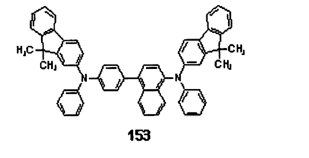
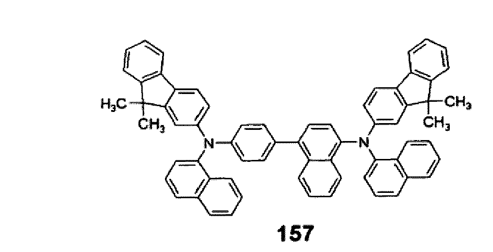
- Nonlimiting examples of suitable compounds satisfying Formula 1 included Compounds 1 to 54 and 105 to 242 below (Compounds 55 to 104 are not according to the invention, but useful for understanding the same).
- the compound satisfying Formula 1 is selected from Compounds 1, 2, 3, 32,105,153,157,159,173,184 and 213 above.
- an organic light-emitting device includes a first electrode, a second electrode, and an organic film between the first electrode and the second electrode.
- the organic film includes a compound represented by Formula 1 and may be a hole injection layer or a hole transport layer.
- the organic film may also be a single film having both a hole injection function and a hole transport function.
- the organic film may be an emissive layer.
- the compound represented by Formula 1 may be used as a host material for phosphorescent or fluorescent blue, green, or red color materials.
- the organic film may be a hole injection layer or a hole transport layer.
- the first electrode may be an anode, and the second electrode may be a cathode.
- the first electrode may be a cathode, and the second electrode may be an anode.
- the organic light emitting device may further include, whenever necessary or desired, at least one additional layer selected from hole injection layers, hole transport layers, electron blocking layers, emissive layers, hole blocking layers, electron transport layers, and electron injection layers.
- the organic light emitting device may include a double-layered organic layer including two of the above organic layers, whenever necessary or desired.
- an organic light emitting device may have a first electrode/hole injection layer/emissive layer/second electrode structure, a first electrode/hole injection layer/hole transport layer/emissive layer/electron transport layer/second electrode structure, or a first electrode/hole injection layer/hole transport layer/emissive layer/electron transport layer/electron injection layer/second electrode structure.
- the organic light emitting device may have a first electrode/single organic film with both hole injection and hole transport functions/emissive layer/electron transport layer/second electrode structure, or a first electrode/single organic film with both hole injection and hole transport functions/emissive layer/electron transport layer/electron injection layer/second electrode structure.
- the organic light emitting devices according to embodiments of the present invention may be used in various applications such as top emission type organic light emitting devices and bottom emission type organic light emitting devices.
- an organic light emitting device includes a substrate, a first electrode (e.g., an anode), a hole injection layer, a hole transport layer, an emissive layer, an electron transport layer, and a second electrode (e.g., a cathode).
- a first electrode e.g., an anode
- a hole injection layer e.g., an electron transport layer
- a hole transport layer e.g., an emissive layer
- an electron transport layer e.g., a cathode
- the first electrode is formed by applying a first electrode forming material having a high work function on a substrate by deposition or sputtering.
- the first electrode may either be an anode or a cathode.
- the substrate may be any conventional substrate used in organic light emitting devices.
- the substrate may be a glass substrate or a transparent plastic substrate, both of which have excellent mechanical strength, thermal stability, transparency, surface planarity, convenience in handling, and water resistance.
- the first electrode forming material may include a material selected from indium tin oxide (ITO), indium zinc oxide (IZO), tin oxide (SnO 2 ), zinc oxide (ZnO), Al, Ag, Mg, and combinations thereof.
- the first electrode forming material has excellent conductivity and may be used to form a transparent or reflective electrode.
- the hole injection layer may be formed on the first electrode using a variety of methods such as vacuum deposition, spin coating, casting, and Langmuir-Blodget (LB) deposition.
- the deposition conditions may differ depending on the compound used as the material for the HIL and the desired structure and thermal properties of the HIL.
- the deposition conditions may include a deposition temperature ranging from about 100 to about 500°C, a vacuum pressure ranging from about 10 -8 to about 10 -3 torr, a deposition rate ranging from about 0.01 to about 100 ⁇ /sec, and a film thickness ranging from about 10 ⁇ to about 5 ⁇ m.
- the coating conditions may differ depending on the compound used as the material for the HIL and the desired structure and thermal properties of the HIL.
- the spin coating conditions may include a coating speed ranging from about 2000 to about 5000 rpm, and a heat-treatment temperature for removing a solvent after coating ranging from about 80 to about 200°C.
- the HIL material may be the compound represented by Formula 1, as described above.
- any known HIL material may be used.
- a phthalocyanine compound such as copper phthalocyanine
- TCTA shown below
- m-MTDATA shown below
- m-MTDAPB starburst-type amine derivatives
- Soluble conductive polymers such as Pani/DBSA (polyaniline/dodecylbenzenesulfonic acid), PEDOT/PSS (poly(3,4-ethylenedioxythiophene)/poly(4-styrenesulfonate), Pani/CSA (polyaniline /camphor sulfonic acid), and PANI/PSS (polyaniline)/poly (4-styrene-sulfonate) may also be used.
- Pani/DBSA polyaniline/dodecylbenzenesulfonic acid
- PEDOT/PSS poly(3,4-ethylenedioxythiophene)/poly(4-styrenesulfonate
- Pani/CSA polyaniline /camphor sulfonic acid
- PANI/PSS polyaniline
- the thickness of the HIL may range from about 100 to about 10000 ⁇ . For example, in one embodiment, the thickness may range from about 100 to about 1000 ⁇ . If the thickness of the HIL is less than about 100 ⁇ , the hole injection properties may deteriorate, and if the thickness of the HIL is greater than about 10000 ⁇ , the driving voltage may increase.
- the hole transport layer may be formed on the HIL by a variety of methods, such as vacuum deposition, spin coating, casting, and LB deposition.
- the deposition or coating conditions may differ depending on the compounds used, but may generally include the deposition and coating conditions described above with respect to the HIL.
- the HTL material may be a compound represented by Formula 1 described above.
- any known HTL material may be used, for example, carbazole derivatives (such as N-phenylcarbazole and polyvinylcarbazole) and conventional amine derivatives having condensed aromatic condensed rings (such as 4,4'-bis[N-(1-naphthyl)-N-phenylamino]biphenyl (NPB), N,N'-bis(3-methylphenyl)- N,N'-diphenyl-[1,1-biphenyl]-4,4'-diamine (TPD)(shown below), and N,N'-di(naphthalene-1-yl)-N,N'-diphenyl benzidine ( ⁇ -NPD) (shown below)).
- carbazole derivatives such as N-phenylcarbazole and polyvinylcarbazole
- conventional amine derivatives having condensed aromatic condensed rings such as 4,
- the thickness of the HTL may range from about 50 to about 1000 ⁇ . For example, in one embodiment, the thickness ranges from about 100 to about 600 ⁇ . If the thickness of the HTL is less than about 50 ⁇ , the hole transporting properties may deteriorate, and if the thickness of the HTL is greater than about 1000 ⁇ , the driving voltage may increase.
- the emissive layer may be formed on the HTL by a variety of methods, such as vacuum deposition, spin coating, casting, and LB deposition.
- the deposition or coating conditions may differ depending on the compounds used, but may generally include the deposition and coating conditions described above with respect to the HIL.
- the EML may include a compound represented by Formula 1 described above.
- the compound represented by Formula 1 may be used as a host.
- the EML may be formed using a variety of known light emitting materials, and may be formed using known hosts and dopants.
- the dopant may be any known dopant and may be either a phosphorescent dopant or a fluorescent dopant.
- Nonlimiting examples of suitable hosts include Alq 3 , CPB (4,4'-N,N'-dicarbazole-biphenyl), PVK (poly(n-vinylcarbazole)), DSA (distyrylarylene), or IDE215 (from Idemitsu Co.).
- Nonlimiting examples of suitable phosphorescent dopants include IDE102, IDE105 and IDE118 (available from Idemitsu Co.).
- suitable fluorescent dopants include Ir(ppy) 3 (ppy is an abbreviation of phenylpyridine)(green), 4,6-F2(ppy) 2 Irpic, TEB002 (from Cobion Co.), PtOEP (platinum(II) octaethylporphyrin), compounds represented by Formula 3 below, Firpric (shown below), and RD61 (which is a red fluorescent dopant from UDC Co.).
- the content of the dopant may range from about 0.1 to about 20 parts by weight based on 100 parts by weight of the EML forming material (i.e., the total weight of the host and the dopant is 100 parts by weight). In one embodiment, for example, the dopant is present in an amount ranging from about 0.5 to about 12 parts by weight based on 100 parts by weight of the EML forming material. If the dopant is present in an amount less than about 0.1 parts by weight based on the total weight of the host and the dopant, the effect of adding the dopant is minute. If the dopant is present in an amount greater than about 20 parts by weight based on the total weight of the host and the dopant, concentration extinction (e.g. concentration quenching) of both the phosphorescent and the fluorescent components may occur.
- concentration extinction e.g. concentration quenching
- the thickness of the EML may range from about 100 to about 1000 ⁇ . In one embodiment, for example, the thickness ranges from about 200 to about 600 ⁇ . If the thickness of the EML is less than about 100 ⁇ , the light emitting properties may deteriorate, and if the thickness of the EML is greater than about 1000 ⁇ , the driving voltage may increase.
- a hole blocking layer may be formed on the EML to prevent triplet excitons or holes from diffusing to the electron transport layer (not shown in FIG. 1 ).
- the HBL material is not particularly limited, and may be selected from any known HBL materials. Nonlimiting examples of suitable HBL materials include oxadiazole derivatives, triazole derivatives, phenathroline derivatives, Balq and BCP.
- the thickness of the HBL may range from about 50 to about 1000 ⁇ . In one embodiment, for example, the thickness may range from about 100 to about 300 ⁇ . If the thickness of the HBL is less than about 50 ⁇ , the hole-blocking properties may deteriorate, and if the thickness of the HBL is greater than about 1000 ⁇ , the driving voltage may increase.
- the electron transport layer may be formed on the HBL or on the EML by a variety of methods, such as vacuum deposition, spin coating, and casting.
- the deposition or coating conditions may differ depending on the compounds used, but may generally include the deposition and coating conditions described above with respect to the HIL.
- the ETL material is not particularly limited, and may be selected from any known ETL forming materials.
- suitable ETL materials include quinoline derivatives, and in particular, tris(8-quinolinolate)aluminum (Alq 3 ) and TAZ.
- the thickness of the ETL may range from about 100 to about 1000 ⁇ . In one embodiment, for example, the thickness ranges from about 100 to about 500 ⁇ . If the thickness of the ETL is less than about 100 ⁇ , the electron transporting properties may deteriorate, and if the thickness of the EML is greater than about 1000 ⁇ , the driving voltage may increase.
- an electron injection layer may be deposited on the ETL.
- the EIL facilitates the injection of electrons from the cathode.
- the EIL may be formed of any known EIL material, nonlimiting examples of which include LiF, NaCl, CsF, Li 2 O, and BaO.
- the deposition or coating conditions may differ depending on the compounds used, but may generally include the deposition and coating conditions described above with respect to the HIL.
- the thickness of the EIL may range from about 1 to about 100 ⁇ . In one embodiment, for example, the thickness may range from about 5 to about 90 ⁇ . If the thickness of the EIL is less than about 1 ⁇ , the electron injecting properties may deteriorate, and if the thickness of the EIL is greater than about 100 ⁇ , the driving voltage may increase.
- the second electrode may be formed on the EIL by any suitable method, such as vacuum deposition or sputtering.
- the second electrode may be a cathode or an anode.
- the material for forming the second electrode may be a metal, an alloy, or an electrically conductive compound with a low work function. Nonlimiting examples of such materials include Li, Mg, Al, Al-Li, Ca, Mg-In, and Mg-Ag.
- a transparent cathode such as ITO or IZO may be used in order to obtain a top emission device.
- the organic light emitting device may be used in many applications, including flat panel display devices such as passive matrix organic light emitting display devices and active matrix organic light emitting display devices.
- the first electrode on the substrate is a pixel electrode and is electrically connected to a source electrode or a drain electrode of a thin film transistor.
- the organic light-emitting device may also be included in a flat panel display device having a double-sided screen.
- Compound 32 was synthesized by the reaction pathway represented by Reaction Scheme 4 below.
- An anode was prepared by cutting a Coming 15 ⁇ cm 2 (1200 ⁇ ) ITO glass substrate to a size of 50 mm ⁇ 50 mm ⁇ 0.7 mm, sonicating for 5 minutes using isopropyl alcohol and deionized water, and then irradiating with UV light for 30 minutes and exposing to ozone to clean. Then, the prepared anode was installed on a vacuum deposition apparatus.
- Compound 1 was vacuum deposited on the anode to a thickness of 600 ⁇ to form an HIL, and 4,4'-bis[N-(1-naphthyl)-N-phenylamino]biphenyl (NPB) as a hole transporting compound was vacuum deposited on the HIL to a thickness of 300 ⁇ to form a HTL.
- NPB 4,4'-bis[N-(1-naphthyl)-N-phenylamino]biphenyl
- a blue fluorescent host (IDE215 from Idemitsu Co.) and a blue fluorescent dopant (IDE118 from Idemitsu Co.) were deposited simultaneously (at a weight ratio of 98:2) on the HTL to form an EML with a thickness of 200 ⁇ .
- IDE215 from Idemitsu Co.
- IDE118 from Idemitsu Co.
- Alq 3 was deposited on the EML to a thickness of 300 ⁇ to form an ETL, and a halogenated alkaline metal LiF was deposited to a thickness of 10 ⁇ on the ETL to form an EIL.
- A1 was vacuum deposited on the EIL to a thickness of 3000 ⁇ (cathode), thereby completing the manufacture of an organic light emitting device.
- the device had a driving voltage of 6.68 V, a high emission brightness of 7,898 cd/m 2 , color coordinates of (0.144, 0.232), and an emission efficiency of 7.9 cd/A, at a current density of 100 mA/cm 2 ,
- An organic light-emitting device was prepared as in Example 1, except that Compound 2 was used instead of Compound 1 when forming the HIL.
- the device had a driving voltage of 6.72 V, a high emission brightness of 7,733 cd/m 2 , color coordinates of (0.144, 0.236), and an emission efficiency of 7.73cd/A, at a current density of 100 mA/cm 2 .
- An organic light-emitting device was prepared as in Example 1, except that Compound 3 was used instead of Compound 1 when forming the HIL.
- the device had a driving voltage of 6.79 V, a high emission brightness of 7,490 cd/m 2 , color coordinates of (0.143, 0.237), and an emission efficiency of 7.49 cd/A, at a current density of 100 mA/cm 2 .
- An organic light-emitting device was prepared as in Example 1, except that Compound 32 was used instead of Compound 1 when forming the HIL.
- the device had a driving voltage of 6.64 V, a high emission brightness of 7,289 cd/m 2 , color coordinates of (0.145, 0.241), and an emission efficiency of 7.29 cd/A, at a current density of 100 mA/cm 2 .
- An organic light-emitting device was prepared as in Example 1, except that Compound 105 was used instead of Compound 1 when forming the HIL.
- the device had a driving voltage of 6.75 V, a high emission brightness of 7,406 cd/m 2 , color coordinates of (0.145, 0.236), and an emission efficiency of 7.41 cd/A, at a current density of 100 mA/cm 2 .
- An anode was prepared by cutting a Corning 15 ⁇ cm 2 (1200 ⁇ ) ITO glass substrate to a size of 50 mm ⁇ 50 mm ⁇ 0.7 mm, sonicating for 5 minutes using isopropyl alcohol and deionized water, and then irradiating with UV light for 30 minutes and exposing to ozone to clean. Then, the prepared anode was installed on a vacuum deposition apparatus.
- 2-TNATA (shown below) was vacuum deposited on the anode to a thickness of 600 ⁇ to form a HIL, and then Compound 153 was vacuum deposited on the HIL to a thickness of 300 ⁇ to form a HTL.
- a blue fluorescent host (IDE215 from Idemitsu Co.) and a blue fluorescent dopant (IDE118 from Idemitsu Co.) were deposited simultaneously (at a weight ratio of 98:2) on the HTL to form an EML with a thickness of 200 ⁇ .
- IDE215 from Idemitsu Co.
- IDE118 from Idemitsu Co.
- Alq 3 was deposited on the EML to a thickness of 300 ⁇ to form an ETL, and a halogenated alkaline metal LiF was deposited on the ETL to a thickness of 10 ⁇ to form an EIL.
- A1 was vacuum deposited on the EIL to a thickness of 3000 ⁇ (cathode), thereby completing the manufacture of an organic light-emitting device.
- the device had a driving voltage of 6.57 V, a high emission brightness of 8,340 cd/m 2 , color coordinates of (0.144, 0.233), and an emission efficiency of 8.34 cd/A, at a current density of 100mA/cm 2 .
- An organic light-emitting device was prepared as in Example 6, except that Compound 173 was used instead of Compound 153 when forming the HTL.
- the device had a driving voltage of 6.72 V, a high emission brightness of 7,950 cd/m 2 , color coordinates of (0.143, 0.231), and an emission efficiency of 7.95 cd/A, at a current density of 100 mA/cm 2 .
- An organic light emitting device was prepared as in Example 6, except that Compound 184 was used instead of Compound 153 when forming the HTL.
- the device had a current density of 100 mA/cm 2 , a driving voltage of 6.83 V, a high emission brightness of 7,890 cd/m 2 , color coordinates of (0.144, 0.229), and an emission efficiency of 7.89 cd/A at a current density of 100 mA/cm 2 .
- An organic light emitting device was prepared as in Example 6, except that Compound 213 was used instead of Compound 153 when forming the HTL.
- the device had a driving voltage of 7.05 V, a high emission brightness of 7,896 cd/m 2 , color coordinates of (0.145, 0.234), and an emission efficiency of 7.90 cd/A at a current density of 100 mA/cm 2 .
- An organic light emitting device was prepared as in Example 1, except that a material represented by the structure below was used instead of Compound 1 when forming the HIL.
- the device had a driving voltage of 6.18 V, an emission brightness of 7,134cd/m 2 , color coordinates of (0.144, 0.237), and an emission efficiency of 7.13 cd/A at a current density of 100 mA/cm 2 .
- An organic light emitting device was prepared as in Example 1, except that 2-TNATA (shown below) was used instead of Compound 1 when forming the HIL.
- the device had a driving voltage of 7.45 V, an emission brightness of 6,102cd/m 2 , color coordinates of (0.144, 0.232), and an emission efficiency of 6.1 cd/A at a current density of 100 mA/cm 2 .
- the compounds represented by Formula 1 according to embodiments of the present invention had superior device properties than the compounds used in the Comparative Examples.
- the device prepared with Compound 1 had a lower driving voltage, improved efficiency, and a life span 1.5 times longer (see FIG. 2 ). This is due to an effect caused by the naphthyl group located in the core structure of Compound 1 (as opposed to a phenyl group), which functions to stabilize the radicals produced during hole injection or transportation.
- the compounds represented by Formula 1 according to embodiments of the present invention when used as hole injection or hole transportation materials of organic light emitting devices, the compounds represented by Formula 1 according to embodiments of the present invention have lower driving voltages compared to the conventional material, 2-TNATA.
- the compounds represented by Formula 1 according to embodiments of the present invention showed excellent I-V-L properties with 30% or more improved efficiency (See FIG. 3 ), and can be used to prepare organic light emitting devices with low voltage, high efficiency, high brightness, and long life span.
- the compounds represented by Formula 1 according to embodiments of the present invention have excellent electrical properties and charge transporting characteristics, and are therefore useful as materials for hole injection layers, hole transport layers, and emission layers of phosphorescent and fluorescent devices for emitting light of all colors, including red, green, blue, and white. Using these compounds, an organic light-emitting device with high efficiency, low driving voltage, and high brightness can be prepared.
Landscapes
- Chemical & Material Sciences (AREA)
- Organic Chemistry (AREA)
- Engineering & Computer Science (AREA)
- Materials Engineering (AREA)
- Physics & Mathematics (AREA)
- Spectroscopy & Molecular Physics (AREA)
- Optics & Photonics (AREA)
- Electroluminescent Light Sources (AREA)
- Organic Low-Molecular-Weight Compounds And Preparation Thereof (AREA)
- Indole Compounds (AREA)
Claims (15)
- Composé représenté par la formule 1 :
 X est sélectionné parmi le groupe constitué de structures substituées et non substituées représentées par :
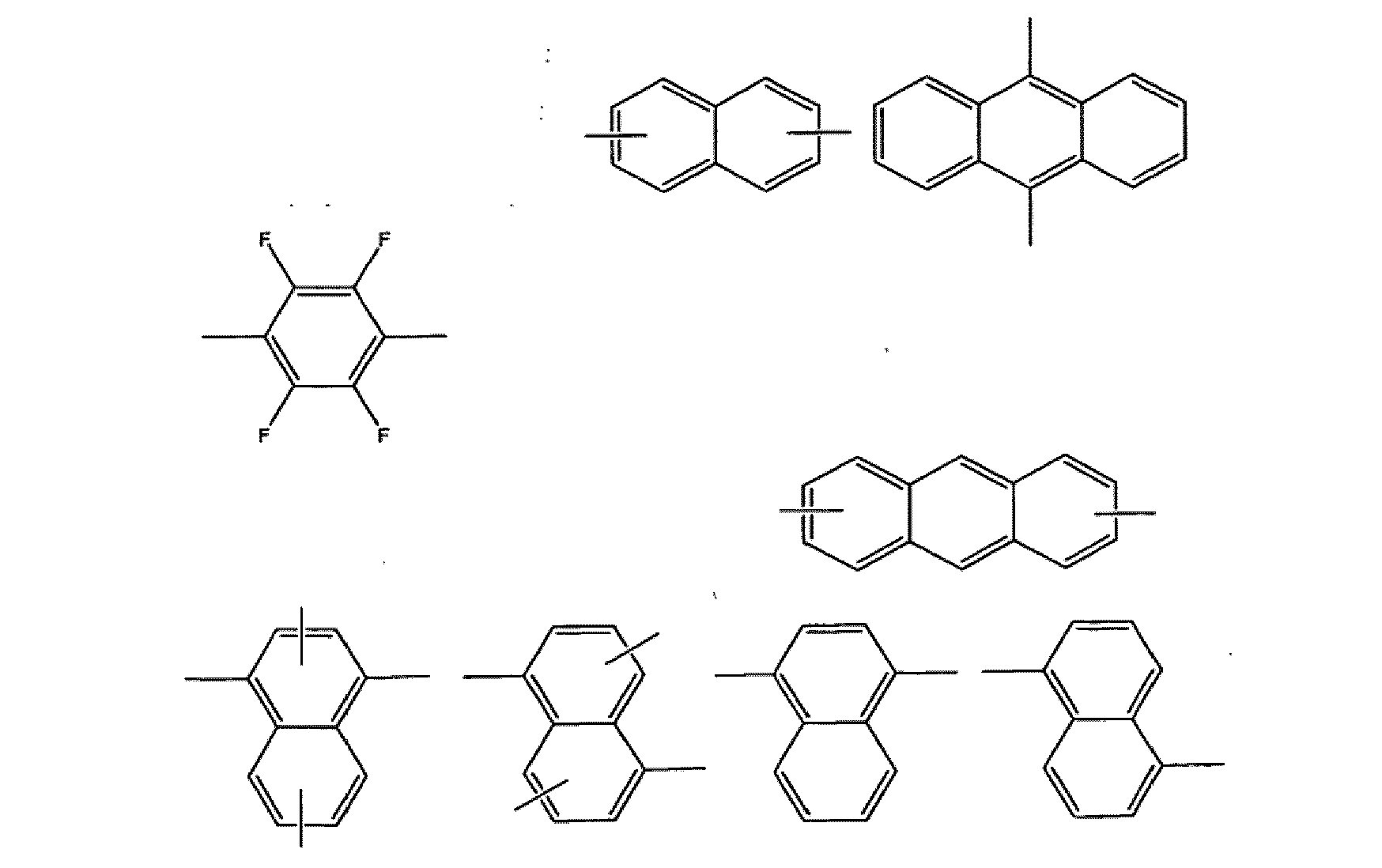 Ar1 et Ar2 sont respectivement sélectionnés indépendamment l'un de l'autre parmi le groupe constitué des groupes phényle, biphényle, naphtyle et anthracényle substitués et non substitués, où, pour des groupes Ar1 et Ar2 substitués, le ou les cycle(s) aromatique(s) de Ar1 et Ar2 est/sont substitué(s) par un à trois groupes sélectionnés parmi le groupe constitué des groupes alkyle en C1 à C4, des groupes alcoxy en C1 à C5, du groupe cyano, du groupe amino, du groupe phénoxy, du groupe phényle, du groupe N,N-diphénylamino, et d'atomes d'halogène ; etY est sélectionné parmi le groupe constitué de matériaux représentés par les formules 2 et 3
 dans lesquelles R1, R2, R3, R4 et R5 sont respectivement sélectionnés indépendamment les uns des autres parmi le groupe constitué de l'hydrogène, des groupes alkyle en C1 à C10 substitués et non substitués, des groupes aryle en C6 à C20 substitués et non substitués, des groupes alcoxy en C1 à C10 substitués et non substitués, du fluor, du groupe cyano, et du groupe amino ; ou au moins deux groupes R adjacents sélectionnés parmi le groupe constitué de R1, R2, R3, R4 et R5 peuvent se lier les uns aux autres pour former un cycle carbone saturé ou insaturé.
 - Composé selon la revendication 1, qui est représenté par la formule 4 :
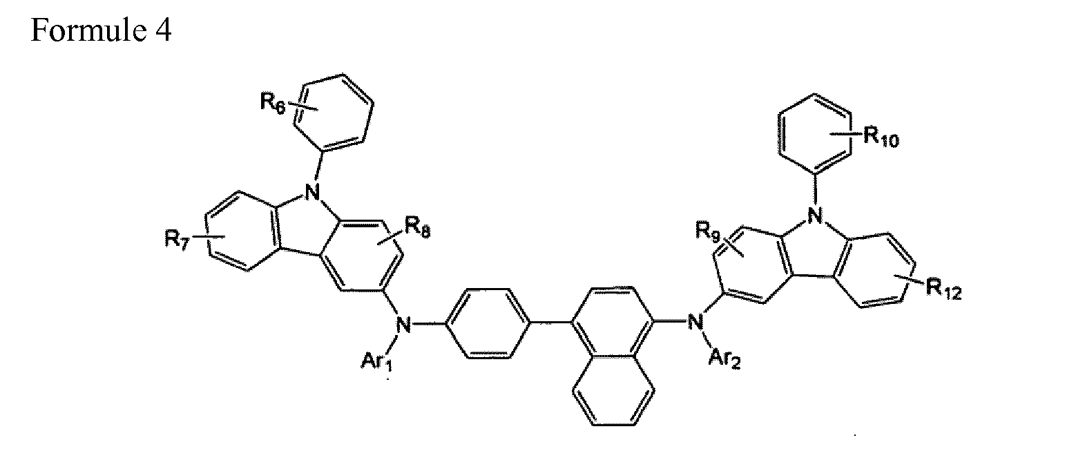 dans laquelle R6, R7, R8, R9, R10, R11 et R12 sont respectivement sélectionnés indépendamment les uns des autres parmi le groupe constitué de l'hydrogène, des groupes alkyle en C1 à C10 substitués et non substitués, les groupes aryle en C6 à C20 substitués et non substitués, des groupes alcoxy en C1 à C10 substitués et non substitués, du fluor, du groupe cyano, et du groupe amino ; ou au moins deux groupes R adjacents sélectionnés parmi le groupe constitué de R6, R7, R8, R9, R10, R11 et R12 peuvent se lier les uns aux autres pour former un cycle carbone saturé ou insaturé, etdans laquelle Ar1 et Ar2 sont respectivement tels que définis selon la revendication 1.
 - Composé selon la revendication 1, qui est représenté par la formule 5 :
 dans laquelle R6, R7, R8, R9, R10, R11 et R12 sont respectivement sélectionnés indépendamment les uns des autres parmi le groupe constitué de l'hydrogène, des groupes alkyle en C1 à C10 substitués et non substitués, des groupes aryle en C6 à C20 substitués et non substitués, des groupes alcoxy en C1 à C10 substitués et non substitués, du fluor, du groupe cyano, et du groupe amino, ou au moins deux groupes R adjacents sélectionnés parmi le groupe constitué de R6, R7, R8, R9, R10, R11 et R12 peuvent se lier les uns aux autres pour former un cycle carbone saturé ou insaturé ; etAr1 et Ar2 sont respectivement tels que définis selon la revendication 1.
 - Composé selon la revendication 1, qui est représenté par la formule 6 :
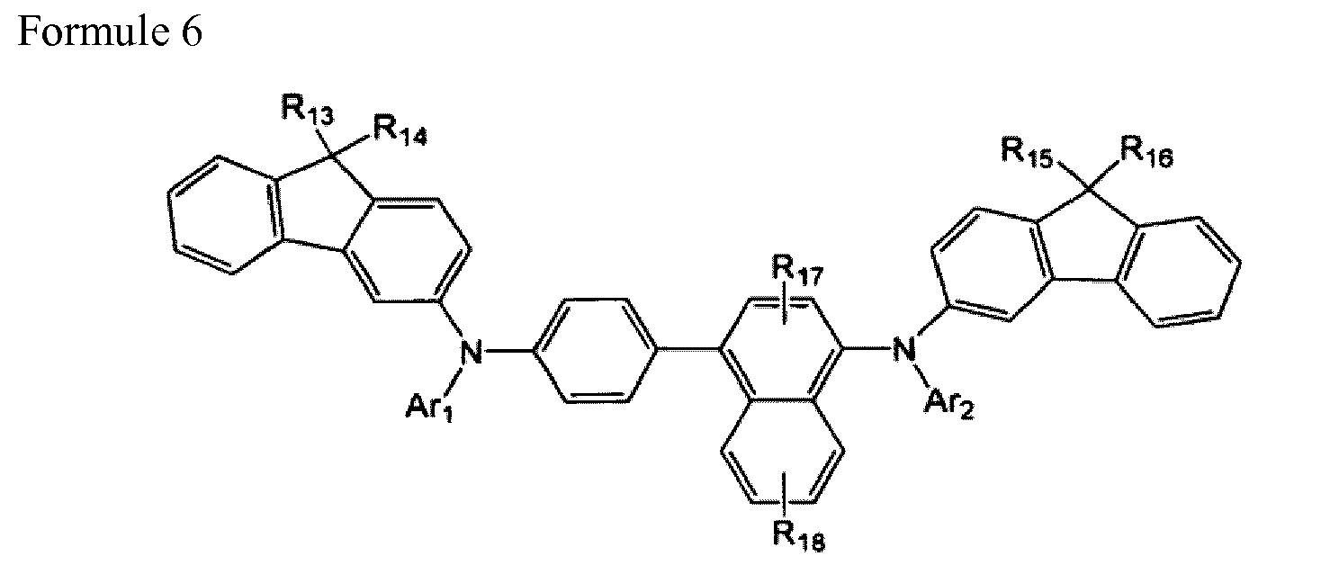 dans laquelle R13, R14, R15, R16, R17 et R18 sont respectivement sélectionnés indépendamment les uns des autres parmi le groupe constitué de l'hydrogène, des groupes alkyle en C1 à C10 substitués et non substitués, des groupes aryle en C6 à C20 substitués et non substitués, des groupes alcoxy en C1 à C10 substitués et non substitués, du fluor, du groupe cyano, et du groupe amino ; ou au moins deux groupes R adjacents sélectionnés parmi le groupe constitué de R13, R14, R15, R16, R17 et R18 peuvent se lier les uns aux autres pour former un cycle carbone saturé ou insaturé ; etAr1 et Ar2 sont respectivement tels que définis selon la revendication 1.
 - Composé selon la revendication 1, qui est représenté par la formule 7 :
 dans laquelle R13, R14, R15, R16, R17 et R18 sont respectivement sélectionnés indépendamment les uns des autres parmi le groupe constitué de l'hydrogène, des groupes alkyle en C1 à C10 substitués et non substitués, des groupes aryle en C6 à C20 substitués et non substitués, des groupes alcoxy en C1 à C10 substitués et non substitués, du fluor, du groupe cyano, et du groupe amino ; ou au moins deux groupes R adjacents sélectionnés parmi le groupe constitué de R13, R14, R15, R16, R17 et R18 peuvent se lier les uns aux autres pour former un cycle carbone saturé ou insaturé ; etAr1 et Ar2 sont respectivement tels que définis selon la revendication 1.
 - Composé selon la revendication 1, qui est représenté par la formule 8 :
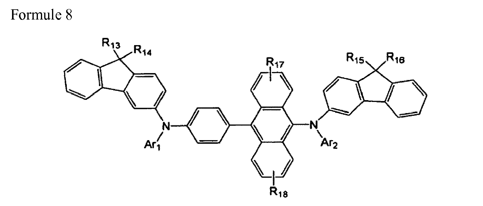 dans laquelle R13, R14, R15, R16, R17 et R18 sont respectivement sélectionnés indépendamment les uns des autres parmi le groupe constitué de l'hydrogène, des groupes alkyle en C1 à C10 substitués et non substitués, des groupes aryle en C6 à C20 substitués et non substitués, des groupes alcoxy en C1 à C10 substitués et non substitués, du fluor, des groupes cyano, et des groupes amino ; ou au moins deux groupes R adjacents sélectionnés parmi le groupe constitué de R13, R14, R15, R16, R17 et R18 peuvent se lier les uns aux autres pour former un cycle carbone saturé ou insaturé ; etAr1 et Ar2 sont respectivement tels que définis selon la revendication 1.
 - Composé selon l'une quelconque des revendications 1 à 6, sélectionné parmi le groupe constitué des composés 1, 2, 3, 32, 105, 153, 157, 159, 173, 184 et 213 :




- Dispositif électroluminescent organique comprenant une première électrode, une seconde électrode, et un film organique entre la première électrode et la seconde électrode,
dans lequel le film organique comprend un composé selon l'une quelconque des revendications 1 à 7. - Dispositif électroluminescent organique selon la revendication 8, dans lequel le film organique comprend une couche sélectionnée parmi le groupe constitué de couches d'injection de trous et de couches de transport de trous.
- Dispositif électroluminescent organique selon la revendication 8 ou 9, dans lequel le film organique comprend un film unique comprenant une couche d'injection de trous et une couche de transport de trous.
- Dispositif électroluminescent organique selon l'une quelconque des revendications 8 à 10, dans lequel le film organique comprend une couche émissive.
- Dispositif électroluminescent organique selon la revendication 11, dans lequel la couche émissive comprend le composé selon la revendication 1 en tant qu'hôte, et comprend en outre un dopant sélectionné parmi le groupe constitué des dopants phosphorescents et fluorescents.
- Dispositif électroluminescent organique selon l'une quelconque des revendications 8 à 12, dans lequel le dispositif comprend une structure sélectionnée parmi le groupe constitué des structures première électrode/couche d'injection de trous/couche émissive/seconde électrode, des structures première électrode/couche d'injection de trous/couche de transport de trous/couche émissive/couche de transport d'électrons/seconde électrode, et des structures première électrode/couche d'injection de trous/couche de transport de trous/couche émissive/couche de transport d'électrons/couche d'injection d'électrons/seconde électrode.
- Dispositif électroluminescent organique selon la revendication 13, comprenant en outre au moins une couche parmi une couche de blocage de trous et une couche de blocage d'électrons.
- Dispositif d'affichage à écran plat comprenant un dispositif électroluminescent organique selon l'une quelconque des revendications 8 à 14, dans lequel la première électrode du dispositif électroluminescent organique est électriquement raccordée à une électrode de source ou à une électrode de drain d'un transistor en couches minces.
Applications Claiming Priority (1)
| Application Number | Priority Date | Filing Date | Title |
|---|---|---|---|
| KR1020080012206A KR100964223B1 (ko) | 2008-02-11 | 2008-02-11 | 유기 발광 소자 및 이를 구비한 평판 표시 장치 |
Publications (2)
| Publication Number | Publication Date |
|---|---|
| EP2093271A1 EP2093271A1 (fr) | 2009-08-26 |
| EP2093271B1 true EP2093271B1 (fr) | 2015-10-21 |
Family
ID=40510030
Family Applications (1)
| Application Number | Title | Priority Date | Filing Date |
|---|---|---|---|
| EP09250339.0A Ceased EP2093271B1 (fr) | 2008-02-11 | 2009-02-11 | Composé pour la formation d'un film organique, dispositif électroluminescent organique et dispositif à écran plan l'incluant |
Country Status (6)
| Country | Link |
|---|---|
| US (1) | US8394511B2 (fr) |
| EP (1) | EP2093271B1 (fr) |
| JP (1) | JP5015182B2 (fr) |
| KR (1) | KR100964223B1 (fr) |
| CN (1) | CN101508670B (fr) |
| TW (1) | TWI397517B (fr) |
Families Citing this family (41)
| Publication number | Priority date | Publication date | Assignee | Title |
|---|---|---|---|---|
| KR100787425B1 (ko) * | 2004-11-29 | 2007-12-26 | 삼성에스디아이 주식회사 | 페닐카바졸계 화합물 및 이를 이용한 유기 전계 발광 소자 |
| US8188315B2 (en) | 2004-04-02 | 2012-05-29 | Samsung Mobile Display Co., Ltd. | Organic light emitting device and flat panel display device comprising the same |
| US8021765B2 (en) * | 2004-11-29 | 2011-09-20 | Samsung Mobile Display Co., Ltd. | Phenylcarbazole-based compound and organic electroluminescent device employing the same |
| KR100846607B1 (ko) * | 2007-05-16 | 2008-07-16 | 삼성에스디아이 주식회사 | 유기 발광 소자 |
| CN101679207B (zh) | 2007-06-01 | 2014-05-28 | E.I.内穆尔杜邦公司 | 用于深蓝色发光应用的* |
| CN101918512B (zh) | 2007-06-01 | 2014-09-24 | E.I.内穆尔杜邦公司 | 绿色发光材料 |
| KR20090120699A (ko) * | 2008-05-20 | 2009-11-25 | 삼성모바일디스플레이주식회사 | 페닐카바졸계 화합물, 이를 포함하는 유기 발광 소자 및이를 구비한 평판 표시 장치 |
| KR101050459B1 (ko) * | 2008-09-03 | 2011-07-20 | 삼성모바일디스플레이주식회사 | 플루오렌 화합물 및 이를 이용한 유기 전계 발광 장치 |
| KR20100070979A (ko) * | 2008-12-18 | 2010-06-28 | 동우 화인켐 주식회사 | 비대칭 구조의 유기전기발광소자용 아릴아민유도체, 그 제조방법, 이를 포함하는 유기전기발광소자용 유기박막재료 및 이를 이용한 유기 전기발광소자 |
| TW201038532A (en) | 2008-12-19 | 2010-11-01 | Du Pont | Anthracene compounds for luminescent applications |
| US8531100B2 (en) | 2008-12-22 | 2013-09-10 | E I Du Pont De Nemours And Company | Deuterated compounds for luminescent applications |
| KR100994118B1 (ko) * | 2009-01-13 | 2010-11-15 | 삼성모바일디스플레이주식회사 | 유기 발광 소자 및 그 제조 방법 |
| US8759818B2 (en) | 2009-02-27 | 2014-06-24 | E I Du Pont De Nemours And Company | Deuterated compounds for electronic applications |
| WO2010114583A1 (fr) | 2009-04-03 | 2010-10-07 | E. I. Du Pont De Nemours And Company | Matériaux électroactifs |
| JP5567675B2 (ja) | 2009-08-13 | 2014-08-06 | イー・アイ・デュポン・ドウ・ヌムール・アンド・カンパニー | クリセン誘導体材料 |
| WO2011040939A1 (fr) | 2009-09-29 | 2011-04-07 | E. I. Du Pont De Nemours And Company | Composés deutérés pour des applications luminescentes |
| TW201114771A (en) | 2009-10-29 | 2011-05-01 | Du Pont | Deuterated compounds for electronic applications |
| KR101352116B1 (ko) * | 2009-11-24 | 2014-01-14 | 엘지디스플레이 주식회사 | 백색 유기 발광 소자 |
| US8617720B2 (en) | 2009-12-21 | 2013-12-31 | E I Du Pont De Nemours And Company | Electroactive composition and electronic device made with the composition |
| TW201229010A (en) * | 2010-12-13 | 2012-07-16 | Du Pont | Electroactive materials |
| JP5727038B2 (ja) | 2010-12-20 | 2015-06-03 | イー・アイ・デュポン・ドウ・ヌムール・アンド・カンパニーE.I.Du Pont De Nemours And Company | 電子技術応用のための組成物 |
| KR101983019B1 (ko) * | 2011-08-03 | 2019-05-28 | 메르크 파텐트 게엠베하 | 전자 소자용 물질 |
| CN103304540B (zh) * | 2012-03-09 | 2016-08-03 | 海洋王照明科技股份有限公司 | 磷光主体材料、其制备方法和电致发光器件 |
| KR101990553B1 (ko) * | 2012-04-17 | 2019-06-19 | 삼성디스플레이 주식회사 | 신규한 유기 발광 소자용 화합물 및 이를 포함한 유기 발광 소자 |
| KR102079249B1 (ko) * | 2012-06-12 | 2020-02-20 | 삼성디스플레이 주식회사 | 신규한 유기 발광 소자용 화합물 및 이를 포함한 유기 발광 소자 |
| JP6208424B2 (ja) | 2012-12-05 | 2017-10-04 | 三星ディスプレイ株式會社Samsung Display Co.,Ltd. | フッ素置換されたアリール基を有するアミン誘導体、それを含む有機el材料及びそれを用いた有機el素子 |
| KR101666781B1 (ko) * | 2013-06-28 | 2016-10-17 | 엘지디스플레이 주식회사 | 유기 발광 소자 |
| KR102044866B1 (ko) * | 2013-08-21 | 2019-11-15 | 삼성디스플레이 주식회사 | 헤테로고리 화합물 및 이를 포함한 유기 발광 소자 |
| CN105016968B (zh) * | 2015-07-07 | 2017-04-05 | 河南省商业科学研究所有限责任公司 | 一种2‑溴‑9,9‑二苯基芴的合成方法 |
| EP3133663B1 (fr) * | 2015-08-18 | 2022-06-15 | Novaled GmbH | Amides métalliques destinés à être utilisés dans une couche d'injection de trous pour une diode électroluminescente organique (oled) |
| CN105085163B (zh) * | 2015-09-06 | 2017-04-12 | 河南省商业科学研究所有限责任公司 | 2‑溴‑9,9‑二苯基芴的合成方法 |
| CN105085162B (zh) * | 2015-09-06 | 2017-04-05 | 河南省商业科学研究所有限责任公司 | 一锅法制备2‑溴‑9,9‑二苯基芴 |
| CN105895820B (zh) * | 2016-06-21 | 2019-01-22 | 武汉华星光电技术有限公司 | 有机发光器件及其显示器 |
| KR102608415B1 (ko) | 2018-04-27 | 2023-12-01 | 삼성디스플레이 주식회사 | 다이아민 화합물을 포함한 유기 발광 소자 및 다이아민 화합물 |
| KR102630639B1 (ko) | 2018-06-20 | 2024-01-30 | 삼성디스플레이 주식회사 | 다이아민 화합물을 포함한 유기 발광 소자 및 다이아민 화합물 |
| KR102797542B1 (ko) | 2019-02-13 | 2025-04-21 | 삼성디스플레이 주식회사 | 유기 발광 소자 |
| CN110105165A (zh) * | 2019-06-12 | 2019-08-09 | 黑龙江省科学院石油化学研究院 | 一种高纯度1,4-二溴萘的制备方法 |
| CN114075115A (zh) * | 2020-08-20 | 2022-02-22 | 江苏三月科技股份有限公司 | 一种胺类化合物和包含该化合物的有机电致发光器件 |
| US12256634B2 (en) | 2020-09-02 | 2025-03-18 | Samsung Display Co., Ltd. | Arylamine compound, light-emitting device including the same, and electronic apparatus including the light-emitting device |
| KR102897917B1 (ko) * | 2020-09-02 | 2025-12-10 | 삼성디스플레이 주식회사 | 아릴아민 화합물, 이를 포함한 발광 소자 및 상기 발광 소자를 포함한 전자 장치 |
| CN115850022B (zh) * | 2022-12-27 | 2025-08-22 | 郑州圣壹新材料科技有限公司 | 一种9,9-二甲基-2-溴芴的合成方法 |
Citations (5)
| Publication number | Priority date | Publication date | Assignee | Title |
|---|---|---|---|---|
| JPH1135532A (ja) * | 1997-05-19 | 1999-02-09 | Canon Inc | 有機化合物及び該有機化合物を用いた発光素子 |
| EP1661888A1 (fr) * | 2004-11-29 | 2006-05-31 | Samsung SDI Co., Ltd. | Composé contenant un phenylcarbazole et dispositif organiques électroluminiscent l'utilisant |
| JP2007126439A (ja) * | 2005-10-07 | 2007-05-24 | Toyo Ink Mfg Co Ltd | カルバゾール含有アミン化合物およびその用途 |
| US20070231503A1 (en) * | 2004-04-02 | 2007-10-04 | Hwang Seok-Hwan | Organic light emitting device and flat panel display device comprising the same |
| EP1862524A1 (fr) * | 2006-05-29 | 2007-12-05 | Samsung SDI Co., Ltd. | Dispositif électroluminescent organique et dispositif d'affichage à écran plat le comprenant |
Family Cites Families (46)
| Publication number | Priority date | Publication date | Assignee | Title |
|---|---|---|---|---|
| US4356429A (en) | 1980-07-17 | 1982-10-26 | Eastman Kodak Company | Organic electroluminescent cell |
| JP2846571B2 (ja) | 1994-02-25 | 1999-01-13 | 出光興産株式会社 | 有機エレクトロルミネッセンス素子 |
| US5550066A (en) | 1994-12-14 | 1996-08-27 | Eastman Kodak Company | Method of fabricating a TFT-EL pixel |
| JP3564859B2 (ja) * | 1996-04-01 | 2004-09-15 | 東洋インキ製造株式会社 | 有機エレクトロルミネッセンス素子用材料およびそれを使用した有機エレクトロルミネッセンス素子 |
| JPH10199674A (ja) | 1996-11-15 | 1998-07-31 | Sanyo Electric Co Ltd | 有機エレクトロルミネッセンス素子の駆動方法、有機エレクトロルミネッセンス装置及び表示装置 |
| US6517957B1 (en) * | 1997-05-19 | 2003-02-11 | Canon Kabushiki Kaisha | Organic compound and electroluminescent device using the same |
| JP3985311B2 (ja) * | 1997-10-20 | 2007-10-03 | チッソ株式会社 | アミン誘導体及びそれを用いた有機電界発光素子 |
| JP3838766B2 (ja) | 1997-11-06 | 2006-10-25 | 三井化学株式会社 | 有機電界発光素子 |
| JPH11329734A (ja) | 1998-03-10 | 1999-11-30 | Mitsubishi Chemical Corp | 有機電界発光素子 |
| EP1009043A3 (fr) | 1998-12-09 | 2002-07-03 | Eastman Kodak Company | Dispositif électroluminescent comprenant une couche transportant des trous d'hydrocarbures polyphényles |
| US6465115B2 (en) | 1998-12-09 | 2002-10-15 | Eastman Kodak Company | Electroluminescent device with anthracene derivatives hole transport layer |
| JP4573923B2 (ja) | 1999-04-27 | 2010-11-04 | 三井化学株式会社 | アミン化合物 |
| JP2001209331A (ja) | 2000-01-27 | 2001-08-03 | Tdk Corp | 薄膜表示装置 |
| JP2002252089A (ja) | 2001-02-26 | 2002-09-06 | Bando Chem Ind Ltd | 両面発光型有機エレクトロルミネッセンス素子 |
| GB0117377D0 (en) | 2001-07-17 | 2001-09-05 | Opsys Ltd | "Tertiary diamines containing heterocyclic groups and their use in organic electroluminescent devices" |
| JP4477799B2 (ja) | 2001-09-03 | 2010-06-09 | 三井化学株式会社 | アミン化合物および該化合物を有する有機電界発光素子 |
| DE10203328A1 (de) | 2002-01-28 | 2003-08-07 | Syntec Ges Fuer Chemie Und Tec | Neue Triarylamin-Derivate mit raumfüllenden Flügelgruppen und ihre Einsatz in elektro-fotografischen und organischen elektrolumineszenten Vorrichtungen |
| KR20030093016A (ko) | 2002-06-01 | 2003-12-06 | 삼성에스디아이 주식회사 | 유기 전계발광 소자 |
| JP4122901B2 (ja) * | 2002-08-28 | 2008-07-23 | 富士ゼロックス株式会社 | 有機電界発光素子 |
| JP4221973B2 (ja) | 2002-08-28 | 2009-02-12 | 富士ゼロックス株式会社 | 有機電界発光素子 |
| JP2004103467A (ja) | 2002-09-11 | 2004-04-02 | Mitsubishi Chemicals Corp | 有機電界発光素子 |
| US20040140757A1 (en) | 2003-01-17 | 2004-07-22 | Eastman Kodak Company | Microcavity OLED devices |
| JP4177707B2 (ja) | 2003-03-27 | 2008-11-05 | 三井化学株式会社 | アミン化合物および該化合物を含有する有機電界発光素子 |
| JP3877692B2 (ja) | 2003-03-28 | 2007-02-07 | 三洋電機株式会社 | 有機エレクトロルミネッセンス素子およびその製造方法 |
| JP2005029000A (ja) | 2003-07-11 | 2005-02-03 | Honda Motor Co Ltd | フィラーパイプの配管構造 |
| US7049741B2 (en) | 2004-01-27 | 2006-05-23 | Eastman Kodak Company | Organic light emitting diode with improved light emission through substrate |
| KR100537621B1 (ko) | 2004-02-02 | 2005-12-19 | 삼성에스디아이 주식회사 | 이리듐 화합물 및 이를 이용한 유기 전계 발광 소자 |
| JP2005294504A (ja) | 2004-03-31 | 2005-10-20 | Nippon Chemicon Corp | 固体電解コンデンサの製造方法 |
| JP4585786B2 (ja) | 2004-04-01 | 2010-11-24 | キヤノン株式会社 | 発光素子及び表示装置 |
| KR100573137B1 (ko) | 2004-04-02 | 2006-04-24 | 삼성에스디아이 주식회사 | 플루오렌계 화합물 및 이를 이용한 유기 전계 발광 소자 |
| KR100669716B1 (ko) | 2004-07-14 | 2007-01-16 | 삼성에스디아이 주식회사 | 페닐카르바졸 화합물 및 이를 이용한 유기 전계 발광 소자 |
| KR100721554B1 (ko) | 2004-07-22 | 2007-05-23 | 삼성에스디아이 주식회사 | 유기 전계 발광 소자 및 그의 제조 방법 |
| JP4782791B2 (ja) | 2004-09-22 | 2011-09-28 | ドーサン・コーポレーション | 三原色光を利用する白色有機電界発光素子 |
| US7358538B2 (en) | 2004-10-28 | 2008-04-15 | Zheng-Hong Lu | Organic light-emitting devices with multiple hole injection layers containing fullerene |
| US8021765B2 (en) | 2004-11-29 | 2011-09-20 | Samsung Mobile Display Co., Ltd. | Phenylcarbazole-based compound and organic electroluminescent device employing the same |
| CN101090887B (zh) * | 2004-12-28 | 2010-09-29 | 株式会社半导体能源研究所 | 蒽衍生物、使用它的发光元件和使用它的发光器件 |
| JP5311712B2 (ja) * | 2004-12-28 | 2013-10-09 | 株式会社半導体エネルギー研究所 | アントラセン誘導体とそれを用いた発光素子、発光装置 |
| JP5089063B2 (ja) | 2005-03-23 | 2012-12-05 | 株式会社半導体エネルギー研究所 | 複合材料および複合材料を用いた発光素子並びに発光装置 |
| US20070003785A1 (en) * | 2005-06-30 | 2007-01-04 | Eastman Kodak Company | Electroluminescent devices containing benzidine derivatives |
| EP1917243B1 (fr) | 2005-07-14 | 2012-02-15 | Semiconductor Energy Laboratory Co., Ltd. | Dérivé de carbazole, matériau d'élément émettant de la lumière, élément émettant de la lumière et objet électronique obtenu en utilisant |
| JP4169085B2 (ja) | 2005-10-07 | 2008-10-22 | 東洋インキ製造株式会社 | カルバゾール含有アミン化合物及びその用途 |
| US20070134512A1 (en) | 2005-12-13 | 2007-06-14 | Eastman Kodak Company | Electroluminescent device containing an anthracene derivative |
| US8993805B2 (en) * | 2006-04-13 | 2015-03-31 | Tosoh Corporation | Benzofluorene compound and use thereof |
| WO2008010377A1 (fr) | 2006-07-21 | 2008-01-24 | Toyo Ink Manufacturing Co., Ltd. | Composé aminé contenant un carbazole et son utilisation |
| JP5133259B2 (ja) | 2006-11-24 | 2013-01-30 | 出光興産株式会社 | 芳香族アミン誘導体及びそれを用いた有機エレクトロルミネッセンス素子 |
| WO2009084268A1 (fr) | 2007-12-28 | 2009-07-09 | Idemitsu Kosan Co., Ltd. | Dérivés d'amines aromatiques et dispositifs organiques électroluminescents employant ces derniers |
-
2008
- 2008-02-11 KR KR1020080012206A patent/KR100964223B1/ko not_active Expired - Fee Related
- 2008-12-16 US US12/336,459 patent/US8394511B2/en active Active
-
2009
- 2009-02-06 CN CN2009100051680A patent/CN101508670B/zh not_active Expired - Fee Related
- 2009-02-09 TW TW98104021A patent/TWI397517B/zh not_active IP Right Cessation
- 2009-02-09 JP JP2009027510A patent/JP5015182B2/ja not_active Expired - Fee Related
- 2009-02-11 EP EP09250339.0A patent/EP2093271B1/fr not_active Ceased
Patent Citations (5)
| Publication number | Priority date | Publication date | Assignee | Title |
|---|---|---|---|---|
| JPH1135532A (ja) * | 1997-05-19 | 1999-02-09 | Canon Inc | 有機化合物及び該有機化合物を用いた発光素子 |
| US20070231503A1 (en) * | 2004-04-02 | 2007-10-04 | Hwang Seok-Hwan | Organic light emitting device and flat panel display device comprising the same |
| EP1661888A1 (fr) * | 2004-11-29 | 2006-05-31 | Samsung SDI Co., Ltd. | Composé contenant un phenylcarbazole et dispositif organiques électroluminiscent l'utilisant |
| JP2007126439A (ja) * | 2005-10-07 | 2007-05-24 | Toyo Ink Mfg Co Ltd | カルバゾール含有アミン化合物およびその用途 |
| EP1862524A1 (fr) * | 2006-05-29 | 2007-12-05 | Samsung SDI Co., Ltd. | Dispositif électroluminescent organique et dispositif d'affichage à écran plat le comprenant |
Also Published As
| Publication number | Publication date |
|---|---|
| JP5015182B2 (ja) | 2012-08-29 |
| US20090200928A1 (en) | 2009-08-13 |
| TWI397517B (zh) | 2013-06-01 |
| CN101508670A (zh) | 2009-08-19 |
| TW200940482A (en) | 2009-10-01 |
| JP2009185030A (ja) | 2009-08-20 |
| US8394511B2 (en) | 2013-03-12 |
| KR20090086756A (ko) | 2009-08-14 |
| KR100964223B1 (ko) | 2010-06-17 |
| CN101508670B (zh) | 2013-05-15 |
| EP2093271A1 (fr) | 2009-08-26 |
Similar Documents
| Publication | Publication Date | Title |
|---|---|---|
| EP2093271B1 (fr) | Composé pour la formation d'un film organique, dispositif électroluminescent organique et dispositif à écran plan l'incluant | |
| KR101771531B1 (ko) | 스피로 화합물 및 이를 포함하는 유기전계발광소자 | |
| CN113227066B (zh) | 有机发光元件用化合物及包含该化合物的长寿命的有机发光元件 | |
| KR101792175B1 (ko) | 스피로 화합물 및 이를 포함하는 유기전계발광소자 | |
| KR101779913B1 (ko) | 스피로 화합물 및 이를 포함하는 유기전계발광소자 | |
| KR101825381B1 (ko) | 스피로 화합물 및 이를 포함하는 유기전계발광소자 | |
| KR101771528B1 (ko) | 스피로 화합물 및 이를 포함하는 유기전계발광소자 | |
| TWI382972B (zh) | 苯基咔唑化合物、含苯基咔唑化合物之有機發光元件及含該有機發光元件之平面顯示裝置 | |
| KR101529157B1 (ko) | 유기 발광 화합물 및 이를 이용한 유기 발광 소자 | |
| KR101050459B1 (ko) | 플루오렌 화합물 및 이를 이용한 유기 전계 발광 장치 | |
| KR101861263B1 (ko) | 안트라센 유도체 및 이를 포함하는 유기전계발광소자. | |
| KR101321500B1 (ko) | 유기 전계 발광 화합물 및 이를 이용한 유기 전계 발광소자 | |
| KR101328974B1 (ko) | 유기 전계 발광 화합물 및 이를 이용한 유기 전계 발광소자 | |
| KR101559430B1 (ko) | 유기 발광 화합물 및 이를 이용한 유기 발광 소자 | |
| KR101453873B1 (ko) | 사이클로펜타페난트렌계 화합물 및 이를 이용한 유기 발광소자 | |
| CN100441578C (zh) | 含咪唑环的化合物和有机电致发光显示器 | |
| KR101791023B1 (ko) | 축합방향족 화합물 및 이를 포함하는 유기전계발광소자 | |
| KR101320382B1 (ko) | 유기 발광 화합물 및 이를 구비한 유기 발광 소자 | |
| CN108779080B (zh) | 新型化合物及包含它的有机发光元件 | |
| KR101779915B1 (ko) | 축합 아릴아민계 화합물 및 이를 포함하는 유기전계발광소자 | |
| KR101809898B1 (ko) | 헤테로아릴아민 유도체 및 이를 포함하는 유기전계발광소자 | |
| KR101780699B1 (ko) | 스피로 화합물 및 이를 포함하는 유기전계발광소자 | |
| CN101993445A (zh) | 杂环化合物和包括该杂环化合物的有机发光装置 | |
| KR101759481B1 (ko) | 스피로 화합물 및 이를 포함하는 유기전계발광소자 | |
| CN101238194B (zh) | 茚衍生物以及使用该衍生物的有机发光二极管 |
Legal Events
| Date | Code | Title | Description |
|---|---|---|---|
| PUAI | Public reference made under article 153(3) epc to a published international application that has entered the european phase |
Free format text: ORIGINAL CODE: 0009012 |
|
| 17P | Request for examination filed |
Effective date: 20090217 |
|
| AK | Designated contracting states |
Kind code of ref document: A1 Designated state(s): AT BE BG CH CY CZ DE DK EE ES FI FR GB GR HR HU IE IS IT LI LT LU LV MC MK MT NL NO PL PT RO SE SI SK TR |
|
| AX | Request for extension of the european patent |
Extension state: AL BA RS |
|
| AKX | Designation fees paid |
Designated state(s): DE FR GB HU IT |
|
| 17Q | First examination report despatched |
Effective date: 20110520 |
|
| RAP1 | Party data changed (applicant data changed or rights of an application transferred) |
Owner name: SAMSUNG DISPLAY CO., LTD. |
|
| REG | Reference to a national code |
Ref country code: DE Ref legal event code: R079 Ref document number: 602009034325 Country of ref document: DE Free format text: PREVIOUS MAIN CLASS: C09K0011060000 Ipc: H01L0051000000 |
|
| GRAP | Despatch of communication of intention to grant a patent |
Free format text: ORIGINAL CODE: EPIDOSNIGR1 |
|
| RIC1 | Information provided on ipc code assigned before grant |
Ipc: C09K 11/06 20060101ALI20150415BHEP Ipc: H01L 51/00 20060101AFI20150415BHEP |
|
| INTG | Intention to grant announced |
Effective date: 20150508 |
|
| GRAS | Grant fee paid |
Free format text: ORIGINAL CODE: EPIDOSNIGR3 |
|
| GRAA | (expected) grant |
Free format text: ORIGINAL CODE: 0009210 |
|
| RAP1 | Party data changed (applicant data changed or rights of an application transferred) |
Owner name: SAMSUNG DISPLAY CO., LTD. |
|
| AK | Designated contracting states |
Kind code of ref document: B1 Designated state(s): DE FR GB HU IT |
|
| REG | Reference to a national code |
Ref country code: GB Ref legal event code: FG4D |
|
| REG | Reference to a national code |
Ref country code: DE Ref legal event code: R096 Ref document number: 602009034325 Country of ref document: DE |
|
| REG | Reference to a national code |
Ref country code: FR Ref legal event code: PLFP Year of fee payment: 8 |
|
| PG25 | Lapsed in a contracting state [announced via postgrant information from national office to epo] |
Ref country code: IT Free format text: LAPSE BECAUSE OF FAILURE TO SUBMIT A TRANSLATION OF THE DESCRIPTION OR TO PAY THE FEE WITHIN THE PRESCRIBED TIME-LIMIT Effective date: 20151021 |
|
| REG | Reference to a national code |
Ref country code: DE Ref legal event code: R097 Ref document number: 602009034325 Country of ref document: DE |
|
| PLBE | No opposition filed within time limit |
Free format text: ORIGINAL CODE: 0009261 |
|
| STAA | Information on the status of an ep patent application or granted ep patent |
Free format text: STATUS: NO OPPOSITION FILED WITHIN TIME LIMIT |
|
| 26N | No opposition filed |
Effective date: 20160722 |
|
| REG | Reference to a national code |
Ref country code: FR Ref legal event code: PLFP Year of fee payment: 9 |
|
| REG | Reference to a national code |
Ref country code: FR Ref legal event code: PLFP Year of fee payment: 10 |
|
| PG25 | Lapsed in a contracting state [announced via postgrant information from national office to epo] |
Ref country code: HU Free format text: LAPSE BECAUSE OF FAILURE TO SUBMIT A TRANSLATION OF THE DESCRIPTION OR TO PAY THE FEE WITHIN THE PRESCRIBED TIME-LIMIT; INVALID AB INITIO Effective date: 20090211 |
|
| REG | Reference to a national code |
Ref country code: DE Ref legal event code: R079 Ref document number: 602009034325 Country of ref document: DE Free format text: PREVIOUS MAIN CLASS: H01L0051000000 Ipc: H10K0099000000 |
|
| P01 | Opt-out of the competence of the unified patent court (upc) registered |
Effective date: 20230515 |
|
| PGFP | Annual fee paid to national office [announced via postgrant information from national office to epo] |
Ref country code: DE Payment date: 20240122 Year of fee payment: 16 Ref country code: GB Payment date: 20240122 Year of fee payment: 16 |
|
| PGFP | Annual fee paid to national office [announced via postgrant information from national office to epo] |
Ref country code: FR Payment date: 20240123 Year of fee payment: 16 |
|
| REG | Reference to a national code |
Ref country code: DE Ref legal event code: R119 Ref document number: 602009034325 Country of ref document: DE |
|
| GBPC | Gb: european patent ceased through non-payment of renewal fee |
Effective date: 20250211 |
|
| PG25 | Lapsed in a contracting state [announced via postgrant information from national office to epo] |
Ref country code: DE Free format text: LAPSE BECAUSE OF NON-PAYMENT OF DUE FEES Effective date: 20250902 |
|
| PG25 | Lapsed in a contracting state [announced via postgrant information from national office to epo] |
Ref country code: GB Free format text: LAPSE BECAUSE OF NON-PAYMENT OF DUE FEES Effective date: 20250211 |
|
| PG25 | Lapsed in a contracting state [announced via postgrant information from national office to epo] |
Ref country code: FR Free format text: LAPSE BECAUSE OF NON-PAYMENT OF DUE FEES Effective date: 20250228 |