EP2093645A2 - Regler mit geringer Abschaltspannung - Google Patents
Regler mit geringer Abschaltspannung Download PDFInfo
- Publication number
- EP2093645A2 EP2093645A2 EP08162716A EP08162716A EP2093645A2 EP 2093645 A2 EP2093645 A2 EP 2093645A2 EP 08162716 A EP08162716 A EP 08162716A EP 08162716 A EP08162716 A EP 08162716A EP 2093645 A2 EP2093645 A2 EP 2093645A2
- Authority
- EP
- European Patent Office
- Prior art keywords
- transistors
- field effect
- regulator
- voltage
- current
- Prior art date
- Legal status (The legal status is an assumption and is not a legal conclusion. Google has not performed a legal analysis and makes no representation as to the accuracy of the status listed.)
- Granted
Links
Images
Classifications
-
- G—PHYSICS
- G05—CONTROLLING; REGULATING
- G05F—SYSTEMS FOR REGULATING ELECTRIC OR MAGNETIC VARIABLES
- G05F1/00—Automatic systems in which deviations of an electric quantity from one or more predetermined values are detected at the output of the system and fed back to a device within the system to restore the detected quantity to its predetermined value or values, i.e. retroactive systems
- G05F1/10—Regulating voltage or current
- G05F1/46—Regulating voltage or current wherein the variable actually regulated by the final control device is DC
- G05F1/56—Regulating voltage or current wherein the variable actually regulated by the final control device is DC using semiconductor devices in series with the load as final control devices
Definitions
- the present invention relates to a low drop out voltage regulator.
- Portable electronic devices such as mobile telephones and ultra portable computing devices, frequently use batteries to power them.
- batteries typically use 3.6 volt rechargeable batteries.
- these batteries have a start of life voltage of up to 4.2 volts and, if the user removes the battery whilst keeping the battery charger connected to the device then the voltage provided by some poorly regulated chargers can increase to 5.5 volts or so. Therefore a voltage regulator is provided between the battery and the circuits that it powers in order to ensure that these circuits see a nominally constant voltage.
- These circuits are often digital circuits and are commonly fabricated using sub-micron CMOS integrated circuit manufacturing technology which often has a maximum supply voltage of 3.6 volts or lower.
- an additional circuit may be provided to act as the low drop out voltage regulator, and the additional circuit could use transistors formed in a different technology, it would be advantageous if the voltage regulator could be implemented on the same semi-conductor die as the CMOS integrated circuits.
- a low voltage drop out regulator comprising:
- control transistors are bipolar transistors.
- control transistors could also be formed by a plurality of series connected field effect transistors - in much the same configuration as the first and second field effect transistors are.
- bipolar transistors are parasitic devices formed with the creation of the field effect transistors. Such parasitic transistors have large dimensions compared to the field effect transistors and this gives them break-down voltages in excess of the break-down voltage of the field effect transistors. It should also be noted that other options such as MOS or DMOS devices could be used.
- first and second field effect transistors By placing the first and second field effect transistors in series it becomes possible to share the voltage drop between the regulator input voltage and the regulator output voltage across the transistors. Thus even though the voltage difference between the regulator input voltage and the regulator output voltage may exceed the breakdown voltage for the implementing transistor technology, with care this voltage can be equally shared between the transistors such that each is subjected to less than its breakdown voltage.
- a biasing arrangement is provided for each of the first and second transistors which acts to share the voltage drop equally across them.
- the biasing arrangement is provided by current mirrors.
- the inventors realised that use of a current mirror action would cause voltage stabilisation to occur locally at each of the first and second transistors. As such, one would expect that the transistors are reasonably well matched.
- each of the first and second transistors is the "slave" transistor in a current mirror and the "master" transistors of a current mirror are each controlled to pass the same current.
- the first and second transistors are in series so, by Kirchoffs laws, they have to pass the same current. The interaction that this creates causes the drain-source voltage of each transistor to tend towards the same value, thereby causing the voltage drop between the regulator input and the regulator output to be equally divided between the transistors.
- each of the first and second transistors is in parallel with a bypass arrangement which allows the voltage drop occurring across the transistors to be equally divided between them even when the transistors are switched into a non-conducting state.
- each transistor has a plurality of series connected diodes in parallel with it. The diodes are selected such that the voltage drop across each individual diode junction is less than the 0.6 to 0.7 volts that would normally be expected to turn the diode on. Under these conditions a very small leakage current exists which acts to distribute the voltage between the first and second transistors.
- Other bypass arrangements could be used such as diode connected transistors.
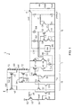
- FIG. 1 is a circuit diagram of a low drop out voltage regulator, generally indicated 2, which serves to accept an unregulated voltage at an input node 4 and to provide a regulated voltage at an output node 6.
- the low drop out voltage regulator consists of three main stages, namely an error amplifier with built in band gap reference, generally designated 10, an inverting amplifier stage (with a compensation capacitor) generally designated 12 and an output driving network generally designated 14.
- the design of the inverting stage is discussed more fully in US 5,631,598 , the teachings of which are incorporated by reference.
- the purpose of the error amplifier is to measure the voltage occurring at the output node 6 and to compare it with a reference voltage and on that basis to output a signal indicating the size and direction of the error between the actual output voltage and a target output voltage.
- This error is amplified within the inverting amplifier 12 and then supplied to the output stage driving network 14.
- the output stage driving network 14 also has the task of ensuring that the voltage dropped by the regulator 2 is equally distributed across the first and second series connected power transistors M1 and M2, respectively.
- the error amplifier and inverter stage can be regarded as forming a controller for controlling the output stage driving network.
- the regulator shown in Figure 1 can be regarded as a "high side" voltage regulator in that the power transistors M1 and M2 are in the positive voltage rail between a power source and a load. It will be appreciated that by an appropriate selection of components the regulator could also be implemented as a low side regulator. However for simplicity the following discussion will focus on the implementation of a high side regulator.
- the first and second power transistors M1 and M2 are P-type field effect transistors connected in series between the voltage regulator input 4 and the voltage regulator output 6. It is often convenient to think of a field effect transistor as being a three terminal device having a source, a drain and a gate.
- the field effect transistor is really a four terminal device comprising a source, a drain, a gate and a back gate.
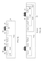
- Figure 2a shows a structure of a PMOS transistor and an NMOS transistor within an integrated circuit.
- the integrated circuit will have a substrate 20 which is doped so as to form a first type of semiconductor, which in this example is a P-type such that we have a P-type substrate.
- a first type of semiconductor which in this example is a P-type such that we have a P-type substrate.
- N-type regions 22 and 24 are formed in the substrate.
- a P-type field effect transistor is more complex. Firstly an N-type well 30 has to be formed within a region of the P-type substrate 20. Having formed the N-type well P-type regions 32 and 34 are formed in order to create the source and drain of the PMOS field effect transistor. The space between the source and drain regions is covered by a metallised gate 36 which, as with the N-type transistor, sits above a layer of insulating material. Thus so far the structure of the P-type field effect transistor mirrors that of the N-type field effect transistor with the addition of the fact that the P-type transistor is formed within an N-type well 30 within the P-type substrate 20.
- a further N-type region 40 is formed within the N-type well 30 such that a voltage can be applied via this further region to bias the parasitic diode formed between the N-type well 30 and the P-type substrate 20 into an off state.
- This further electrode 40 is referred to as a "back gate”.
- NMOS devices are not formed directly within the substrate but instead are isolated from it.
- the NMOS device is fabricated within a P-well 42 which is formed in a deep N-well 44 within the P-type substrate 20.
- parasitic diodes can be formed whenever there is a junction between an N-type and a P-type semiconductor and normally steps are taken to ensure that the voltages applied within the circuit bias these diodes into the off state.
- parasitic bi-polar transistors are created.
- vertical NPN bi-polar transistors can be formed by the interaction between the N-type channels 22 of the NMOS device the P-well 42 an the N-well 44 in Figure 2b with the P-type substrate whereas parasitic PNP transistors can be formed in the vicinity of the P-type field effect transistors.
- parasitic transistors typically have dimensions which are much larger than the CMOS devices that were specifically fabricated within the integrated circuit. The breakdown voltage of the transistor within the integrated circuit depends greatly upon the size of the device and consequently these parasitic bi-polar transistors have much larger breakdown voltages because their physical structure extends over larger distances.
- the transistors M1 and M2 are series connected. However it is important that each transistor sees the same bias and operating conditions in order to ensure good matching. In practical terms, this means that the back gate of the first transistor M1 is connected to the source of the first transistor M1 whereas the back gate of the second transistor M2 is connected to the source of the second transistor M2.
- the source of the first transistor M1 is connected to the input node 4 and the drain of the first transistor M1 is connected to the source of the second transistor M2.
- the drain of the second transistor M2 is connected to the regulator output 6. To aid subsequent understanding of the circuit, it is convenient to think of an intermediate node 50 existing between the drain of the first transistor M1 and the source of the second transistor M2.
- the first transistor M1 is associated with a further P-type field effect transistor M3 such that these devices form a current mirror. Therefore, a source of the transistor M3 is also connected to the input node 4 such that the source voltages of transistors M1 and M3 are identical.
- the gates of the transistors M1 and M3 are connected together such that the gate voltages are identical.
- the gate of transistor M3 is connected to the drain of transistor M3 in order to form the "master" transistor of the current mirror. In use, current is drawn through the transistor M3 and this will cause the gate voltage, and more particularly the gate-source voltage V GS , of M3 to take whatever value is required in order to support that current flow.
- V GS of M3 is supplied to M1 and hence M1 will also try to pass the same current, subject to any scaling between the relative sizes of the transistors.
- M1 is significantly larger than M3, for example a factor of a thousand or so, such that the current that M1 tries to pass will be the same as the current passing through M3 multiplied by the scaling factor.
- M1 is 1000 times larger than M3 then M1 will seek to pass 1000 times the current passing through M3.
- a second current mirror comprising the second transistor M2 and a fourth P-type field effect transistor M4 is also provided.
- a second current mirror has a design similar to that of the first current mirror.
- the source of transistor M4 is connected to the source of transistor M2
- the gate of transistor M4 is connected to the gate of transistor M2
- the gate of transistor M4 is also connected to the drain of the second transistor M4.
- M4's back gate is also connected to its source.
- the current flowing through the transistor M2 of the second current mirror is controlled by the current flowing through M4 but subject to the scaling factor between the transistors M2 and M4.
- current mirrors are matched such that each exhibits the same scaling factor.
- each of the transistors M1 and M2 tries to pass the same current. Inevitably in the absence of any alternative current flow paths they have to pass the same current because they are series connected. However, because each transistor M1 and M2 is seeking to pass the same current and each transistor M1 and M2 has the same gate source voltage, then under ideal conditions each transistor M1 and M2 has the same drain-source voltage, and consequently the voltage drop between the input node 4 and the output node 6 is shared equally between the transistors M1 and M2. In practise slight mismatching between the devices may occur, but this only results in slight differences between the drain source voltages occurring across each transistor.
- a first resistor 52 extends between the gate of transistor M1 and its source whereas a similar resistor 54 is provided for transistor M2.
- the provision of these resistors stops the gate voltage floating when the regulator is off.
- the presence of the resistor 52 allows the drain voltage of M3 to float towards the voltage at the regulator input node 4. This means that a breakdown voltage in excess of the CMOS breakdown voltage could be experienced by a device connected between the drain of M3 and the low voltage rail V SS .
- a device in this position which can be considered as being a control transistor, must also control the current drawn through the third transistor M3.
- the inventors realised that one of the parasitic bi-polar transistors could be placed in this position as it can be used to both control the current passing through M3 and also has the capability to withstand the entirety of the voltage drop that might occur across it when, for example, a power supply is still attached to the portable device but the battery has been removed. Consequently one of the parasitic NPN bi-polar transistors, designated Q1, is connected such that its collector is connected to the drain of the transistor M3 whereas the emitter of Q1 is connected to the low voltage rail V SS , either directly as shown in Figure 1 or potentially via a degenerating resistor.
- a second parasitic NPN bi-polar transistor is connected between the drain of the fourth field effect transistor M4 and the low voltage rail V SS .
- Base terminals of the transistors Q1 and Q2 can be connected together and in a current mirror configuration to the base and collector terminals of a further NPN transistor Q3 such that the current flowing in the first current mirror formed by transistor M1 and M3 is identical to the current flowing in the second current mirror by transistors M3 and M4 because the current flowing in transistors Q1 and Q2 is identical to that flowing in transistor Q3 by virtue of the current mirror action formed around transistors Q1, Q2 and Q3.
- N-type field effect transistors M5 and M6 form the differential input stage with the gate of M5 forming one input to the differential amplifier and the gate of M6 forming the other input.
- the sources of M5 and M6 are connected together and via a constant current sink 60 to the ground or lower voltage supply rail V SS .
- each transistor M5 and M6 is connected to an active load.
- the active load for transistor M5 is formed by a PMOS transistor M7 whose source is connected to the regulator output node 6, whose drain is connected to the drain of transistor M5 and whose gate is also connected to its drain such that the transistor M7 is in a diode connected configuration.
- a similarly configured transistor M8 forms the active load for transistor M6.
- the transistor M7 also forms the "master" transistor for a further current mirror formed between transistor M7 and M9.
- M9 is a P-type field effect transistor whose source is connected to the source of M7 and whose gate is connected to the gate of M7.
- Transistor M9 is provided in series with the collector of transistor Q3 such that M9 controls the amount of current flowing through transistor Q3.
- the error amplifier 10 will now be briefly described. Any error amplifier configuration having either a dual ended or single ended output could be used as, in use, one of the inputs of the differential amplifier formed by M5 and M6 could be tied to a reference voltage.
- the error amplifier comprises three bi-polar NPN transistors Q4, Q5 and Q6 of which Q4 and Q5 are arranged in a current mirror configuration with Q4 acting as the "master".
- a collector of Q4 receives a current from a current source 62 whereas the collector of Q5 receives current from a current source 64.
- the current sources 62 and 64 are matched such that they provide the same current.
- the emitter of Q4 is connected to the source of a P-type field effect transistor whose gate and a drain are connected to Vss.
- the emitter of Q5 is also connected to a source of a P-type field effect transistor whose drain is connected to V SS .
- the gate of this further field effect transistor M11 is connected to a further network comprising resistors r1 to r4, and transistor Q6.
- the transistor Q6 has its emitter connected to the gate of field effect transistor M11 and to V SS via resistor r4.
- the base and collector of transistor Q6 are connected together and via resistor r3 to a node formed between series connected resistors r1 and r2 that extend between the regulator output node 6 and V SS .
- An emitter ratio 1 to N exists between transistors Q4 and Q5.
- V out V t ⁇ L n N r ⁇ 4 ⁇ r ⁇ 3 + r ⁇ 1 r ⁇ 2 r ⁇ 1 + r ⁇ 2 + V be
- the error amplifier 10 measures the voltage V out , compares it with its inherent internal reference voltage, and produces an error voltage which is provided to the gate of M6 and which is compared to a reference which is provided to the gate of M5. Depending on the difference between these voltages, either more current or less current flows through transistors M7, M9, Q3 and hence Q1 and Q2 and ultimately through M1 and M2 such that the voltage of the output node 6 is stabilised towards a target voltage.
- a compensation capacitor C extends between the output node 6 and the voltage provided to the gate of transistor M6.
- transistors M1 and M2 are biased fully off.
- a load remains permanently connected to the regulator, for example because it is integrated into a personal communications device such as a mobile telephone and the load can be represented by a resistor R load optionally in parallel with a capacitor. Therefore in the off condition V out which is the voltage at the output node 6 tends towards V SS .
- V out which is the voltage at the output node 6 tends towards V SS .
- the full unregulated voltage occurring at the input node 4 occurs across the first and second transistors M1 and M2. Therefore even in the off state some precaution must be taken to ensure that the voltage dropped across the series connected transistors M1 and M2 is shared equally between them such that neither exceeds its breakdown voltage.
- each transistor is associated with its own diode stack connected in parallel to it.
- the first diode stack 70 comprises four series connected bypass diodes and similarly the second diode stack 72 also comprises four serially connected bypass diodes.
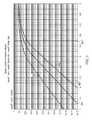
- each diode stack would have to drop 2.1 volts as represented by the vertical line 80.
- the graph also shows a further vertical line 82 at 3.6 volts representing the maximum permissible voltage that may be dropped across either one of the transistors M1 and M2.
- the graph also includes three curves with the curve 84 representing the nominal current flow through the diodes and curves 86 and 88 representing the worst case characteristics as a result of process variation during fabrication and temperature variation.
- the transistors are in series and without the presence of the diode stacks 70 and 72 would have to pass the same current.
- the presence of the diode stacks 70 and 72 now provides additional current flow paths in the event that there is a slight imbalance between the transistors.
- the transistor currents when they are on should be accurately matched because V gs and V bs (back-gate to source voltage) are well matched, but even if they were not then in the worse case scenario represented by line 86 the diode stacks would allow an imbalance of approximately 500 ⁇ A to occur between the current mirrors before either one of the transistors came close to its maximum operating voltage.
- the leakage current is expected to be dominated by leakage through the source and drain junctions. This will not be matched because the source, drain and back-gate voltages of the devices will be different.
- Q8 has its emitter connected to the supply rail V SS and its base connected to its collector such that it forms the "master" transistor of a current mirror involving transistors Q9 and Q10.
- Q9 is connected in parallel with Q1 and Q10 is connected in parallel with Q2. Consequently when a turn on voltage is provided to the node 90 a current defined by resistor 94 flows through Q8 and is mirrored into transistors Q9 and Q10 which turn on thereby enabling a start up current to flow through transistor M3 and transistor M4.
- bias detection circuit 96 which monitors the build up of voltage on the output node 6 and once it has reached a threshold voltage sufficient to guarantee normal operation of the circuits 10 and 12, then the bias circuit 96 outputs a signal on control line 98 which is provided to the gate of the P-type field effect transistor 92 so as to switch the transistor into a non-conducting state thereby turning off current flow through Q8, Q9 and Q10.
Landscapes
- Engineering & Computer Science (AREA)
- Physics & Mathematics (AREA)
- Electromagnetism (AREA)
- General Physics & Mathematics (AREA)
- Radar, Positioning & Navigation (AREA)
- Automation & Control Theory (AREA)
- Continuous-Control Power Sources That Use Transistors (AREA)
- Control Of Electrical Variables (AREA)
Applications Claiming Priority (1)
| Application Number | Priority Date | Filing Date | Title |
|---|---|---|---|
| US12/034,984 US7548051B1 (en) | 2008-02-21 | 2008-02-21 | Low drop out voltage regulator |
Publications (3)
| Publication Number | Publication Date |
|---|---|
| EP2093645A2 true EP2093645A2 (de) | 2009-08-26 |
| EP2093645A3 EP2093645A3 (de) | 2013-12-04 |
| EP2093645B1 EP2093645B1 (de) | 2017-11-01 |
Family
ID=40637853
Family Applications (1)
| Application Number | Title | Priority Date | Filing Date |
|---|---|---|---|
| EP08162716.8A Ceased EP2093645B1 (de) | 2008-02-21 | 2008-08-20 | Regler mit geringer Abschaltspannung |
Country Status (4)
| Country | Link |
|---|---|
| US (1) | US7548051B1 (de) |
| EP (1) | EP2093645B1 (de) |
| CN (1) | CN101515184B (de) |
| TW (1) | TWI369602B (de) |
Families Citing this family (20)
| Publication number | Priority date | Publication date | Assignee | Title |
|---|---|---|---|---|
| US8080983B2 (en) * | 2008-11-03 | 2011-12-20 | Microchip Technology Incorporated | Low drop out (LDO) bypass voltage regulator |
| JP5762205B2 (ja) * | 2011-08-04 | 2015-08-12 | ラピスセミコンダクタ株式会社 | 半導体集積回路 |
| CN103681513B (zh) * | 2013-12-20 | 2016-04-13 | 上海岭芯微电子有限公司 | 集成电路充电驱动器及其制造方法 |
| EP2887174B1 (de) * | 2013-12-20 | 2021-01-13 | Dialog Semiconductor GmbH | CCCV-Verfahren zur Steuerung des Anlaufstroms für LDO |
| US9152841B1 (en) * | 2014-03-24 | 2015-10-06 | Fingerprint Cards Ab | Capacitive fingerprint sensor with improved sensing element |
| CN106793868B (zh) | 2014-04-14 | 2020-06-12 | 爱格升公司 | 高度可调节的桌面工作表面 |
| CN104181970B (zh) * | 2014-08-29 | 2016-05-11 | 电子科技大学 | 一种内嵌基准运算放大器的低压差线性稳压器 |
| CA2999757C (en) | 2015-09-24 | 2020-01-07 | Ergotron, Inc. | Height adjustable device |
| WO2017062589A1 (en) | 2015-10-08 | 2017-04-13 | Ergotron, Inc. | Height adjustable table |
| US9588541B1 (en) * | 2015-10-30 | 2017-03-07 | Qualcomm Incorporated | Dual loop regulator circuit |
| US9791880B2 (en) | 2016-03-16 | 2017-10-17 | Analog Devices Global | Reducing voltage regulator transistor operating temperatures |
| US9946283B1 (en) | 2016-10-18 | 2018-04-17 | Qualcomm Incorporated | Fast transient response low-dropout (LDO) regulator |
| JP6805005B2 (ja) * | 2017-01-30 | 2020-12-23 | エイブリック株式会社 | リーク電流補償回路及び半導体装置 |
| US10411599B1 (en) | 2018-03-28 | 2019-09-10 | Qualcomm Incorporated | Boost and LDO hybrid converter with dual-loop control |
| CN110531826B (zh) * | 2018-05-25 | 2020-09-25 | 光宝科技新加坡私人有限公司 | 低压降分流稳压器 |
| US10444780B1 (en) | 2018-09-20 | 2019-10-15 | Qualcomm Incorporated | Regulation/bypass automation for LDO with multiple supply voltages |
| US10591938B1 (en) | 2018-10-16 | 2020-03-17 | Qualcomm Incorporated | PMOS-output LDO with full spectrum PSR |
| US10545523B1 (en) | 2018-10-25 | 2020-01-28 | Qualcomm Incorporated | Adaptive gate-biased field effect transistor for low-dropout regulator |
| US11372436B2 (en) | 2019-10-14 | 2022-06-28 | Qualcomm Incorporated | Simultaneous low quiescent current and high performance LDO using single input stage and multiple output stages |
| PH12022553246A1 (en) | 2020-07-24 | 2024-02-12 | Qualcomm Inc | Charge pump based low dropout regulator |
Citations (2)
| Publication number | Priority date | Publication date | Assignee | Title |
|---|---|---|---|---|
| EP1635239A1 (de) | 2004-09-14 | 2006-03-15 | Dialog Semiconductor GmbH | Adaptive Vorspannung für einen Strommodi-Spannungsregler |
| US20080007242A1 (en) | 2006-07-07 | 2008-01-10 | Tomokazu Kojima | Power supply circuit |
Family Cites Families (8)
| Publication number | Priority date | Publication date | Assignee | Title |
|---|---|---|---|---|
| FR2494519A1 (fr) * | 1980-11-14 | 1982-05-21 | Efcis | Generateur de courant integre en technologie cmos |
| US4471292A (en) * | 1982-11-10 | 1984-09-11 | Texas Instruments Incorporated | MOS Current mirror with high impedance output |
| EP0943975B1 (de) * | 1998-03-16 | 2005-06-08 | STMicroelectronics S.r.l. | Polarisationsspannungssteuerschaltung für schwebende Senke in einer integrierten Halbleiterschaltung |
| US6188212B1 (en) * | 2000-04-28 | 2001-02-13 | Burr-Brown Corporation | Low dropout voltage regulator circuit including gate offset servo circuit powered by charge pump |
| DE10215084A1 (de) * | 2002-04-05 | 2003-10-30 | Infineon Technologies Ag | Schaltungsanordnung zur Spannungsregelung |
| US6989659B2 (en) * | 2002-09-09 | 2006-01-24 | Acutechnology Semiconductor | Low dropout voltage regulator using a depletion pass transistor |
| CN100514246C (zh) * | 2005-09-16 | 2009-07-15 | 财团法人工业技术研究院 | 低压降线性稳压器 |
| CN200993746Y (zh) * | 2006-12-22 | 2007-12-19 | 崇贸科技股份有限公司 | 低压降稳压器 |
-
2008
- 2008-02-21 US US12/034,984 patent/US7548051B1/en active Active
- 2008-08-20 EP EP08162716.8A patent/EP2093645B1/de not_active Ceased
- 2008-11-18 TW TW097144475A patent/TWI369602B/zh not_active IP Right Cessation
- 2008-11-21 CN CN2008101823320A patent/CN101515184B/zh not_active Expired - Fee Related
Patent Citations (2)
| Publication number | Priority date | Publication date | Assignee | Title |
|---|---|---|---|---|
| EP1635239A1 (de) | 2004-09-14 | 2006-03-15 | Dialog Semiconductor GmbH | Adaptive Vorspannung für einen Strommodi-Spannungsregler |
| US20080007242A1 (en) | 2006-07-07 | 2008-01-10 | Tomokazu Kojima | Power supply circuit |
Non-Patent Citations (1)
| Title |
|---|
| AHMADI: "A full CMOS voltage regulating circuit for bioimplantable applications", 48TH MIDWEST SYMPOSIUM ON CIRCUITS AND SYSTEMS, August 2005 (2005-08-01), pages 988 - 991, XP010893757, DOI: doi:10.1109/MWSCAS.2005.1594269 |
Also Published As
| Publication number | Publication date |
|---|---|
| US7548051B1 (en) | 2009-06-16 |
| CN101515184B (zh) | 2011-03-23 |
| TW200937167A (en) | 2009-09-01 |
| TWI369602B (en) | 2012-08-01 |
| EP2093645B1 (de) | 2017-11-01 |
| CN101515184A (zh) | 2009-08-26 |
| EP2093645A3 (de) | 2013-12-04 |
Similar Documents
| Publication | Publication Date | Title |
|---|---|---|
| EP2093645B1 (de) | Regler mit geringer Abschaltspannung | |
| US6455901B2 (en) | Semiconductor integrated circuit | |
| US6958643B2 (en) | Folded cascode bandgap reference voltage circuit | |
| KR101688661B1 (ko) | 기준 전압 회로 | |
| US6201435B1 (en) | Low-power start-up circuit for a reference voltage generator | |
| US20090302931A1 (en) | Low-power voltage reference | |
| US8026756B2 (en) | Bandgap voltage reference circuit | |
| US9651958B2 (en) | Circuit for regulating startup and operation voltage of an electronic device | |
| KR102038041B1 (ko) | 전원 선택 회로 | |
| US9141125B2 (en) | Bandgap reference voltage generating circuit and electronic system using the same | |
| Yang et al. | A single-chip 60-V bulk charger for series Li-ion batteries with smooth charge-mode transition | |
| US7443199B2 (en) | Circuit arrangement for voltage selection, and method for operating a circuit arrangement for voltage selection | |
| EP2500793B1 (de) | Niederspannungsbezugsstromkreis | |
| US20200064877A1 (en) | Regulator controlled by single transistor and integrated circuit using the same | |
| US20250123642A1 (en) | Cascode voltage regulator circuit | |
| US10423175B2 (en) | Method for providing a voltage reference at a present operating temperature in a circuit | |
| US7053591B2 (en) | Power conversion device with efficient output current sensing | |
| CN118202575A (zh) | 用于mos器件中的泄漏减小的电路和方法 | |
| US20200336141A1 (en) | Supply voltage supervisor | |
| CN1672110A (zh) | 带隙参考电路 | |
| EP3282581A1 (de) | Pufferstufe und steuerschaltung | |
| US20050001672A1 (en) | Double-sided extended drain field effect transistor, and integrated overvoltage and reverse voltage protection circuit that uses the same | |
| US6496040B1 (en) | Trading off gate delay versus leakage current using device stack effect | |
| US6369553B1 (en) | Method and an apparatus for adjusting voltage from a source | |
| US20090160562A1 (en) | Oscillating device |
Legal Events
| Date | Code | Title | Description |
|---|---|---|---|
| PUAI | Public reference made under article 153(3) epc to a published international application that has entered the european phase |
Free format text: ORIGINAL CODE: 0009012 |
|
| AK | Designated contracting states |
Kind code of ref document: A2 Designated state(s): AT BE BG CH CY CZ DE DK EE ES FI FR GB GR HR HU IE IS IT LI LT LU LV MC MT NL NO PL PT RO SE SI SK TR |
|
| AX | Request for extension of the european patent |
Extension state: AL BA MK RS |
|
| PUAL | Search report despatched |
Free format text: ORIGINAL CODE: 0009013 |
|
| AK | Designated contracting states |
Kind code of ref document: A3 Designated state(s): AT BE BG CH CY CZ DE DK EE ES FI FR GB GR HR HU IE IS IT LI LT LU LV MC MT NL NO PL PT RO SE SI SK TR |
|
| AX | Request for extension of the european patent |
Extension state: AL BA MK RS |
|
| RIC1 | Information provided on ipc code assigned before grant |
Ipc: G05F 1/46 20060101AFI20131031BHEP Ipc: G05F 1/56 20060101ALI20131031BHEP |
|
| 17P | Request for examination filed |
Effective date: 20140317 |
|
| RBV | Designated contracting states (corrected) |
Designated state(s): AT BE BG CH CY CZ DE DK EE ES FI FR GB GR HR HU IE IS IT LI LT LU LV MC MT NL NO PL PT RO SE SI SK TR |
|
| AKX | Designation fees paid |
Designated state(s): DE FR GB |
|
| 17Q | First examination report despatched |
Effective date: 20160907 |
|
| GRAP | Despatch of communication of intention to grant a patent |
Free format text: ORIGINAL CODE: EPIDOSNIGR1 |
|
| INTG | Intention to grant announced |
Effective date: 20170526 |
|
| GRAS | Grant fee paid |
Free format text: ORIGINAL CODE: EPIDOSNIGR3 |
|
| GRAA | (expected) grant |
Free format text: ORIGINAL CODE: 0009210 |
|
| AK | Designated contracting states |
Kind code of ref document: B1 Designated state(s): DE FR GB |
|
| REG | Reference to a national code |
Ref country code: GB Ref legal event code: FG4D |
|
| REG | Reference to a national code |
Ref country code: DE Ref legal event code: R096 Ref document number: 602008052729 Country of ref document: DE |
|
| REG | Reference to a national code |
Ref country code: DE Ref legal event code: R097 Ref document number: 602008052729 Country of ref document: DE |
|
| REG | Reference to a national code |
Ref country code: FR Ref legal event code: PLFP Year of fee payment: 11 |
|
| PLBE | No opposition filed within time limit |
Free format text: ORIGINAL CODE: 0009261 |
|
| STAA | Information on the status of an ep patent application or granted ep patent |
Free format text: STATUS: NO OPPOSITION FILED WITHIN TIME LIMIT |
|
| 26N | No opposition filed |
Effective date: 20180802 |
|
| P01 | Opt-out of the competence of the unified patent court (upc) registered |
Effective date: 20230607 |
|
| PGFP | Annual fee paid to national office [announced via postgrant information from national office to epo] |
Ref country code: GB Payment date: 20230828 Year of fee payment: 16 |
|
| PGFP | Annual fee paid to national office [announced via postgrant information from national office to epo] |
Ref country code: FR Payment date: 20230825 Year of fee payment: 16 Ref country code: DE Payment date: 20230829 Year of fee payment: 16 |
|
| REG | Reference to a national code |
Ref country code: DE Ref legal event code: R119 Ref document number: 602008052729 Country of ref document: DE |
|
| GBPC | Gb: european patent ceased through non-payment of renewal fee |
Effective date: 20240820 |
|
| PG25 | Lapsed in a contracting state [announced via postgrant information from national office to epo] |
Ref country code: DE Free format text: LAPSE BECAUSE OF NON-PAYMENT OF DUE FEES Effective date: 20250301 |
|
| PG25 | Lapsed in a contracting state [announced via postgrant information from national office to epo] |
Ref country code: GB Free format text: LAPSE BECAUSE OF NON-PAYMENT OF DUE FEES Effective date: 20240820 |
|
| PG25 | Lapsed in a contracting state [announced via postgrant information from national office to epo] |
Ref country code: FR Free format text: LAPSE BECAUSE OF NON-PAYMENT OF DUE FEES Effective date: 20240831 |