EP2093793A2 - Herstellungsverfahren für ein Halbleiterbauelement - Google Patents
Herstellungsverfahren für ein Halbleiterbauelement Download PDFInfo
- Publication number
- EP2093793A2 EP2093793A2 EP09250234A EP09250234A EP2093793A2 EP 2093793 A2 EP2093793 A2 EP 2093793A2 EP 09250234 A EP09250234 A EP 09250234A EP 09250234 A EP09250234 A EP 09250234A EP 2093793 A2 EP2093793 A2 EP 2093793A2
- Authority
- EP
- European Patent Office
- Prior art keywords
- semiconductor device
- semiconductor chip
- section
- encapsulation resin
- conductor section
- Prior art date
- Legal status (The legal status is an assumption and is not a legal conclusion. Google has not performed a legal analysis and makes no representation as to the accuracy of the status listed.)
- Withdrawn
Links
Images























Classifications
-
- H—ELECTRICITY
- H10—SEMICONDUCTOR DEVICES; ELECTRIC SOLID-STATE DEVICES NOT OTHERWISE PROVIDED FOR
- H10W—GENERIC PACKAGES, INTERCONNECTIONS, CONNECTORS OR OTHER CONSTRUCTIONAL DETAILS OF DEVICES COVERED BY CLASS H10
- H10W74/00—Encapsulations, e.g. protective coatings
- H10W74/01—Manufacture or treatment
- H10W74/016—Manufacture or treatment using moulds
-
- H—ELECTRICITY
- H10—SEMICONDUCTOR DEVICES; ELECTRIC SOLID-STATE DEVICES NOT OTHERWISE PROVIDED FOR
- H10W—GENERIC PACKAGES, INTERCONNECTIONS, CONNECTORS OR OTHER CONSTRUCTIONAL DETAILS OF DEVICES COVERED BY CLASS H10
- H10W40/00—Arrangements for thermal protection or thermal control
- H10W40/70—Fillings or auxiliary members in containers or in encapsulations for thermal protection or control
- H10W40/77—Auxiliary members characterised by their shape
-
- H—ELECTRICITY
- H10—SEMICONDUCTOR DEVICES; ELECTRIC SOLID-STATE DEVICES NOT OTHERWISE PROVIDED FOR
- H10W—GENERIC PACKAGES, INTERCONNECTIONS, CONNECTORS OR OTHER CONSTRUCTIONAL DETAILS OF DEVICES COVERED BY CLASS H10
- H10W40/00—Arrangements for thermal protection or thermal control
- H10W40/70—Fillings or auxiliary members in containers or in encapsulations for thermal protection or control
- H10W40/77—Auxiliary members characterised by their shape
- H10W40/778—Auxiliary members characterised by their shape in encapsulations
-
- H—ELECTRICITY
- H10—SEMICONDUCTOR DEVICES; ELECTRIC SOLID-STATE DEVICES NOT OTHERWISE PROVIDED FOR
- H10W—GENERIC PACKAGES, INTERCONNECTIONS, CONNECTORS OR OTHER CONSTRUCTIONAL DETAILS OF DEVICES COVERED BY CLASS H10
- H10W70/00—Package substrates; Interposers; Redistribution layers [RDL]
- H10W70/40—Leadframes
- H10W70/421—Shapes or dispositions
- H10W70/424—Cross-sectional shapes
- H10W70/427—Bent parts
-
- H—ELECTRICITY
- H10—SEMICONDUCTOR DEVICES; ELECTRIC SOLID-STATE DEVICES NOT OTHERWISE PROVIDED FOR
- H10W—GENERIC PACKAGES, INTERCONNECTIONS, CONNECTORS OR OTHER CONSTRUCTIONAL DETAILS OF DEVICES COVERED BY CLASS H10
- H10W70/00—Package substrates; Interposers; Redistribution layers [RDL]
- H10W70/40—Leadframes
- H10W70/421—Shapes or dispositions
- H10W70/442—Shapes or dispositions of multiple leadframes in a single chip
-
- H—ELECTRICITY
- H10—SEMICONDUCTOR DEVICES; ELECTRIC SOLID-STATE DEVICES NOT OTHERWISE PROVIDED FOR
- H10W—GENERIC PACKAGES, INTERCONNECTIONS, CONNECTORS OR OTHER CONSTRUCTIONAL DETAILS OF DEVICES COVERED BY CLASS H10
- H10W70/00—Package substrates; Interposers; Redistribution layers [RDL]
- H10W70/40—Leadframes
- H10W70/481—Leadframes for devices being provided for in groups H10D8/00 - H10D48/00
-
- H—ELECTRICITY
- H10—SEMICONDUCTOR DEVICES; ELECTRIC SOLID-STATE DEVICES NOT OTHERWISE PROVIDED FOR
- H10W—GENERIC PACKAGES, INTERCONNECTIONS, CONNECTORS OR OTHER CONSTRUCTIONAL DETAILS OF DEVICES COVERED BY CLASS H10
- H10W72/00—Interconnections or connectors in packages
- H10W72/60—Strap connectors, e.g. thick copper clips for grounding of power devices
-
- H—ELECTRICITY
- H10—SEMICONDUCTOR DEVICES; ELECTRIC SOLID-STATE DEVICES NOT OTHERWISE PROVIDED FOR
- H10W—GENERIC PACKAGES, INTERCONNECTIONS, CONNECTORS OR OTHER CONSTRUCTIONAL DETAILS OF DEVICES COVERED BY CLASS H10
- H10W74/00—Encapsulations, e.g. protective coatings
- H10W74/10—Encapsulations, e.g. protective coatings characterised by their shape or disposition
- H10W74/111—Encapsulations, e.g. protective coatings characterised by their shape or disposition the semiconductor body being completely enclosed
-
- H—ELECTRICITY
- H10—SEMICONDUCTOR DEVICES; ELECTRIC SOLID-STATE DEVICES NOT OTHERWISE PROVIDED FOR
- H10W—GENERIC PACKAGES, INTERCONNECTIONS, CONNECTORS OR OTHER CONSTRUCTIONAL DETAILS OF DEVICES COVERED BY CLASS H10
- H10W90/00—Package configurations
-
- H—ELECTRICITY
- H10—SEMICONDUCTOR DEVICES; ELECTRIC SOLID-STATE DEVICES NOT OTHERWISE PROVIDED FOR
- H10W—GENERIC PACKAGES, INTERCONNECTIONS, CONNECTORS OR OTHER CONSTRUCTIONAL DETAILS OF DEVICES COVERED BY CLASS H10
- H10W90/00—Package configurations
- H10W90/811—Multiple chips on leadframes
-
- H—ELECTRICITY
- H10—SEMICONDUCTOR DEVICES; ELECTRIC SOLID-STATE DEVICES NOT OTHERWISE PROVIDED FOR
- H10W—GENERIC PACKAGES, INTERCONNECTIONS, CONNECTORS OR OTHER CONSTRUCTIONAL DETAILS OF DEVICES COVERED BY CLASS H10
- H10W70/00—Package substrates; Interposers; Redistribution layers [RDL]
- H10W70/40—Leadframes
-
- H—ELECTRICITY
- H10—SEMICONDUCTOR DEVICES; ELECTRIC SOLID-STATE DEVICES NOT OTHERWISE PROVIDED FOR
- H10W—GENERIC PACKAGES, INTERCONNECTIONS, CONNECTORS OR OTHER CONSTRUCTIONAL DETAILS OF DEVICES COVERED BY CLASS H10
- H10W72/00—Interconnections or connectors in packages
- H10W72/01—Manufacture or treatment
- H10W72/013—Manufacture or treatment of die-attach connectors
- H10W72/01308—Manufacture or treatment of die-attach connectors using permanent auxiliary members, e.g. using alignment marks
-
- H—ELECTRICITY
- H10—SEMICONDUCTOR DEVICES; ELECTRIC SOLID-STATE DEVICES NOT OTHERWISE PROVIDED FOR
- H10W—GENERIC PACKAGES, INTERCONNECTIONS, CONNECTORS OR OTHER CONSTRUCTIONAL DETAILS OF DEVICES COVERED BY CLASS H10
- H10W72/00—Interconnections or connectors in packages
- H10W72/071—Connecting or disconnecting
- H10W72/073—Connecting or disconnecting of die-attach connectors
-
- H—ELECTRICITY
- H10—SEMICONDUCTOR DEVICES; ELECTRIC SOLID-STATE DEVICES NOT OTHERWISE PROVIDED FOR
- H10W—GENERIC PACKAGES, INTERCONNECTIONS, CONNECTORS OR OTHER CONSTRUCTIONAL DETAILS OF DEVICES COVERED BY CLASS H10
- H10W72/00—Interconnections or connectors in packages
- H10W72/071—Connecting or disconnecting
- H10W72/073—Connecting or disconnecting of die-attach connectors
- H10W72/07311—Treating the bonding area before connecting, e.g. by applying flux or cleaning
-
- H—ELECTRICITY
- H10—SEMICONDUCTOR DEVICES; ELECTRIC SOLID-STATE DEVICES NOT OTHERWISE PROVIDED FOR
- H10W—GENERIC PACKAGES, INTERCONNECTIONS, CONNECTORS OR OTHER CONSTRUCTIONAL DETAILS OF DEVICES COVERED BY CLASS H10
- H10W72/00—Interconnections or connectors in packages
- H10W72/071—Connecting or disconnecting
- H10W72/073—Connecting or disconnecting of die-attach connectors
- H10W72/07321—Aligning
- H10W72/07327—Aligning involving guiding structures, e.g. spacers or supporting members
-
- H—ELECTRICITY
- H10—SEMICONDUCTOR DEVICES; ELECTRIC SOLID-STATE DEVICES NOT OTHERWISE PROVIDED FOR
- H10W—GENERIC PACKAGES, INTERCONNECTIONS, CONNECTORS OR OTHER CONSTRUCTIONAL DETAILS OF DEVICES COVERED BY CLASS H10
- H10W72/00—Interconnections or connectors in packages
- H10W72/071—Connecting or disconnecting
- H10W72/073—Connecting or disconnecting of die-attach connectors
- H10W72/07331—Connecting techniques
-
- H—ELECTRICITY
- H10—SEMICONDUCTOR DEVICES; ELECTRIC SOLID-STATE DEVICES NOT OTHERWISE PROVIDED FOR
- H10W—GENERIC PACKAGES, INTERCONNECTIONS, CONNECTORS OR OTHER CONSTRUCTIONAL DETAILS OF DEVICES COVERED BY CLASS H10
- H10W72/00—Interconnections or connectors in packages
- H10W72/071—Connecting or disconnecting
- H10W72/073—Connecting or disconnecting of die-attach connectors
- H10W72/07331—Connecting techniques
- H10W72/07336—Soldering or alloying
-
- H—ELECTRICITY
- H10—SEMICONDUCTOR DEVICES; ELECTRIC SOLID-STATE DEVICES NOT OTHERWISE PROVIDED FOR
- H10W—GENERIC PACKAGES, INTERCONNECTIONS, CONNECTORS OR OTHER CONSTRUCTIONAL DETAILS OF DEVICES COVERED BY CLASS H10
- H10W72/00—Interconnections or connectors in packages
- H10W72/071—Connecting or disconnecting
- H10W72/073—Connecting or disconnecting of die-attach connectors
- H10W72/07331—Connecting techniques
- H10W72/07337—Connecting techniques using a polymer adhesive, e.g. an adhesive based on silicone or epoxy
-
- H—ELECTRICITY
- H10—SEMICONDUCTOR DEVICES; ELECTRIC SOLID-STATE DEVICES NOT OTHERWISE PROVIDED FOR
- H10W—GENERIC PACKAGES, INTERCONNECTIONS, CONNECTORS OR OTHER CONSTRUCTIONAL DETAILS OF DEVICES COVERED BY CLASS H10
- H10W72/00—Interconnections or connectors in packages
- H10W72/071—Connecting or disconnecting
- H10W72/073—Connecting or disconnecting of die-attach connectors
- H10W72/07331—Connecting techniques
- H10W72/07337—Connecting techniques using a polymer adhesive, e.g. an adhesive based on silicone or epoxy
- H10W72/07338—Connecting techniques using a polymer adhesive, e.g. an adhesive based on silicone or epoxy hardening the adhesive by curing, e.g. thermosetting
-
- H—ELECTRICITY
- H10—SEMICONDUCTOR DEVICES; ELECTRIC SOLID-STATE DEVICES NOT OTHERWISE PROVIDED FOR
- H10W—GENERIC PACKAGES, INTERCONNECTIONS, CONNECTORS OR OTHER CONSTRUCTIONAL DETAILS OF DEVICES COVERED BY CLASS H10
- H10W72/00—Interconnections or connectors in packages
- H10W72/071—Connecting or disconnecting
- H10W72/073—Connecting or disconnecting of die-attach connectors
- H10W72/07351—Connecting or disconnecting of die-attach connectors characterised by changes in properties of the die-attach connectors during connecting
- H10W72/07352—Connecting or disconnecting of die-attach connectors characterised by changes in properties of the die-attach connectors during connecting changes in structures or sizes
-
- H—ELECTRICITY
- H10—SEMICONDUCTOR DEVICES; ELECTRIC SOLID-STATE DEVICES NOT OTHERWISE PROVIDED FOR
- H10W—GENERIC PACKAGES, INTERCONNECTIONS, CONNECTORS OR OTHER CONSTRUCTIONAL DETAILS OF DEVICES COVERED BY CLASS H10
- H10W72/00—Interconnections or connectors in packages
- H10W72/071—Connecting or disconnecting
- H10W72/073—Connecting or disconnecting of die-attach connectors
- H10W72/07351—Connecting or disconnecting of die-attach connectors characterised by changes in properties of the die-attach connectors during connecting
- H10W72/07354—Connecting or disconnecting of die-attach connectors characterised by changes in properties of the die-attach connectors during connecting changes in dispositions
-
- H—ELECTRICITY
- H10—SEMICONDUCTOR DEVICES; ELECTRIC SOLID-STATE DEVICES NOT OTHERWISE PROVIDED FOR
- H10W—GENERIC PACKAGES, INTERCONNECTIONS, CONNECTORS OR OTHER CONSTRUCTIONAL DETAILS OF DEVICES COVERED BY CLASS H10
- H10W72/00—Interconnections or connectors in packages
- H10W72/071—Connecting or disconnecting
- H10W72/076—Connecting or disconnecting of strap connectors
- H10W72/07631—Techniques
- H10W72/07636—Soldering or alloying
-
- H—ELECTRICITY
- H10—SEMICONDUCTOR DEVICES; ELECTRIC SOLID-STATE DEVICES NOT OTHERWISE PROVIDED FOR
- H10W—GENERIC PACKAGES, INTERCONNECTIONS, CONNECTORS OR OTHER CONSTRUCTIONAL DETAILS OF DEVICES COVERED BY CLASS H10
- H10W72/00—Interconnections or connectors in packages
- H10W72/071—Connecting or disconnecting
- H10W72/076—Connecting or disconnecting of strap connectors
- H10W72/07631—Techniques
- H10W72/07637—Techniques using a polymer adhesive, e.g. an adhesive based on silicone or epoxy
-
- H—ELECTRICITY
- H10—SEMICONDUCTOR DEVICES; ELECTRIC SOLID-STATE DEVICES NOT OTHERWISE PROVIDED FOR
- H10W—GENERIC PACKAGES, INTERCONNECTIONS, CONNECTORS OR OTHER CONSTRUCTIONAL DETAILS OF DEVICES COVERED BY CLASS H10
- H10W72/00—Interconnections or connectors in packages
- H10W72/30—Die-attach connectors
- H10W72/321—Structures or relative sizes of die-attach connectors
-
- H—ELECTRICITY
- H10—SEMICONDUCTOR DEVICES; ELECTRIC SOLID-STATE DEVICES NOT OTHERWISE PROVIDED FOR
- H10W—GENERIC PACKAGES, INTERCONNECTIONS, CONNECTORS OR OTHER CONSTRUCTIONAL DETAILS OF DEVICES COVERED BY CLASS H10
- H10W72/00—Interconnections or connectors in packages
- H10W72/30—Die-attach connectors
- H10W72/321—Structures or relative sizes of die-attach connectors
- H10W72/325—Die-attach connectors having a filler embedded in a matrix
-
- H—ELECTRICITY
- H10—SEMICONDUCTOR DEVICES; ELECTRIC SOLID-STATE DEVICES NOT OTHERWISE PROVIDED FOR
- H10W—GENERIC PACKAGES, INTERCONNECTIONS, CONNECTORS OR OTHER CONSTRUCTIONAL DETAILS OF DEVICES COVERED BY CLASS H10
- H10W72/00—Interconnections or connectors in packages
- H10W72/30—Die-attach connectors
- H10W72/341—Dispositions of die-attach connectors, e.g. layouts
- H10W72/347—Dispositions of multiple die-attach connectors
-
- H—ELECTRICITY
- H10—SEMICONDUCTOR DEVICES; ELECTRIC SOLID-STATE DEVICES NOT OTHERWISE PROVIDED FOR
- H10W—GENERIC PACKAGES, INTERCONNECTIONS, CONNECTORS OR OTHER CONSTRUCTIONAL DETAILS OF DEVICES COVERED BY CLASS H10
- H10W72/00—Interconnections or connectors in packages
- H10W72/30—Die-attach connectors
- H10W72/351—Materials of die-attach connectors
-
- H—ELECTRICITY
- H10—SEMICONDUCTOR DEVICES; ELECTRIC SOLID-STATE DEVICES NOT OTHERWISE PROVIDED FOR
- H10W—GENERIC PACKAGES, INTERCONNECTIONS, CONNECTORS OR OTHER CONSTRUCTIONAL DETAILS OF DEVICES COVERED BY CLASS H10
- H10W72/00—Interconnections or connectors in packages
- H10W72/30—Die-attach connectors
- H10W72/351—Materials of die-attach connectors
- H10W72/352—Materials of die-attach connectors comprising metals or metalloids, e.g. solders
-
- H—ELECTRICITY
- H10—SEMICONDUCTOR DEVICES; ELECTRIC SOLID-STATE DEVICES NOT OTHERWISE PROVIDED FOR
- H10W—GENERIC PACKAGES, INTERCONNECTIONS, CONNECTORS OR OTHER CONSTRUCTIONAL DETAILS OF DEVICES COVERED BY CLASS H10
- H10W72/00—Interconnections or connectors in packages
- H10W72/30—Die-attach connectors
- H10W72/351—Materials of die-attach connectors
- H10W72/353—Materials of die-attach connectors not comprising solid metals or solid metalloids, e.g. ceramics
- H10W72/354—Materials of die-attach connectors not comprising solid metals or solid metalloids, e.g. ceramics comprising polymers
-
- H—ELECTRICITY
- H10—SEMICONDUCTOR DEVICES; ELECTRIC SOLID-STATE DEVICES NOT OTHERWISE PROVIDED FOR
- H10W—GENERIC PACKAGES, INTERCONNECTIONS, CONNECTORS OR OTHER CONSTRUCTIONAL DETAILS OF DEVICES COVERED BY CLASS H10
- H10W72/00—Interconnections or connectors in packages
- H10W72/30—Die-attach connectors
- H10W72/381—Auxiliary members
- H10W72/387—Flow barriers
-
- H—ELECTRICITY
- H10—SEMICONDUCTOR DEVICES; ELECTRIC SOLID-STATE DEVICES NOT OTHERWISE PROVIDED FOR
- H10W—GENERIC PACKAGES, INTERCONNECTIONS, CONNECTORS OR OTHER CONSTRUCTIONAL DETAILS OF DEVICES COVERED BY CLASS H10
- H10W72/00—Interconnections or connectors in packages
- H10W72/50—Bond wires
- H10W72/581—Auxiliary members, e.g. flow barriers
-
- H—ELECTRICITY
- H10—SEMICONDUCTOR DEVICES; ELECTRIC SOLID-STATE DEVICES NOT OTHERWISE PROVIDED FOR
- H10W—GENERIC PACKAGES, INTERCONNECTIONS, CONNECTORS OR OTHER CONSTRUCTIONAL DETAILS OF DEVICES COVERED BY CLASS H10
- H10W72/00—Interconnections or connectors in packages
- H10W72/851—Dispositions of multiple connectors or interconnections
- H10W72/874—On different surfaces
- H10W72/886—Die-attach connectors and strap connectors
-
- H—ELECTRICITY
- H10—SEMICONDUCTOR DEVICES; ELECTRIC SOLID-STATE DEVICES NOT OTHERWISE PROVIDED FOR
- H10W—GENERIC PACKAGES, INTERCONNECTIONS, CONNECTORS OR OTHER CONSTRUCTIONAL DETAILS OF DEVICES COVERED BY CLASS H10
- H10W72/00—Interconnections or connectors in packages
- H10W72/90—Bond pads, in general
- H10W72/921—Structures or relative sizes of bond pads
- H10W72/926—Multiple bond pads having different sizes
-
- H—ELECTRICITY
- H10—SEMICONDUCTOR DEVICES; ELECTRIC SOLID-STATE DEVICES NOT OTHERWISE PROVIDED FOR
- H10W—GENERIC PACKAGES, INTERCONNECTIONS, CONNECTORS OR OTHER CONSTRUCTIONAL DETAILS OF DEVICES COVERED BY CLASS H10
- H10W72/00—Interconnections or connectors in packages
- H10W72/90—Bond pads, in general
- H10W72/941—Dispositions of bond pads
- H10W72/944—Dispositions of multiple bond pads
-
- H—ELECTRICITY
- H10—SEMICONDUCTOR DEVICES; ELECTRIC SOLID-STATE DEVICES NOT OTHERWISE PROVIDED FOR
- H10W—GENERIC PACKAGES, INTERCONNECTIONS, CONNECTORS OR OTHER CONSTRUCTIONAL DETAILS OF DEVICES COVERED BY CLASS H10
- H10W74/00—Encapsulations, e.g. protective coatings
-
- H—ELECTRICITY
- H10—SEMICONDUCTOR DEVICES; ELECTRIC SOLID-STATE DEVICES NOT OTHERWISE PROVIDED FOR
- H10W—GENERIC PACKAGES, INTERCONNECTIONS, CONNECTORS OR OTHER CONSTRUCTIONAL DETAILS OF DEVICES COVERED BY CLASS H10
- H10W74/00—Encapsulations, e.g. protective coatings
- H10W74/10—Encapsulations, e.g. protective coatings characterised by their shape or disposition
-
- H—ELECTRICITY
- H10—SEMICONDUCTOR DEVICES; ELECTRIC SOLID-STATE DEVICES NOT OTHERWISE PROVIDED FOR
- H10W—GENERIC PACKAGES, INTERCONNECTIONS, CONNECTORS OR OTHER CONSTRUCTIONAL DETAILS OF DEVICES COVERED BY CLASS H10
- H10W90/00—Package configurations
- H10W90/701—Package configurations characterised by the relative positions of pads or connectors relative to package parts
- H10W90/731—Package configurations characterised by the relative positions of pads or connectors relative to package parts of die-attach connectors
- H10W90/736—Package configurations characterised by the relative positions of pads or connectors relative to package parts of die-attach connectors between a chip and a stacked lead frame, conducting package substrate or heat sink
-
- H—ELECTRICITY
- H10—SEMICONDUCTOR DEVICES; ELECTRIC SOLID-STATE DEVICES NOT OTHERWISE PROVIDED FOR
- H10W—GENERIC PACKAGES, INTERCONNECTIONS, CONNECTORS OR OTHER CONSTRUCTIONAL DETAILS OF DEVICES COVERED BY CLASS H10
- H10W90/00—Package configurations
- H10W90/701—Package configurations characterised by the relative positions of pads or connectors relative to package parts
- H10W90/761—Package configurations characterised by the relative positions of pads or connectors relative to package parts of strap connectors
- H10W90/766—Package configurations characterised by the relative positions of pads or connectors relative to package parts of strap connectors between a chip and a stacked lead frame, conducting package substrate or heat sink
Definitions
- the present invention relates to manufacturing methods of semiconductor devices and in particular to a technique effectively applicable to manufacturing techniques for semiconductor devices of a resin sealed semiconductor package type.
- resin sealed semiconductor packages obtained by sealing a semiconductor chip with an encapsulation resin section.
- a semiconductor chip is sealed in an encapsulation resin section; therefore, the reliability of the semiconductor chip can be enhanced.
- terminals are exposed at the back surface of the encapsulation resin section, the resin sealed semiconductor package can be surface mounted.
- Patent Document 1 discloses a technique related to a semiconductor device.
- This semiconductor device includes: a resin sealing body that seals a semiconductor chip; a first conductive member coupled with a first electrode over a first principal surface of the semiconductor chip; and a second conductive member coupled with a second electrode over a second principal surface of the semiconductor chip on the opposite side to the first principal surface.
- the first conductive member is exposed from the first principal surface of the resin sealing body.
- the second conductive member is exposed from the second principal surface of the resin sealing body on the opposite side to the first principal surface and a side surface.
- Patent Document 2 discloses a technique for exposing a terminal from an encapsulation resin section after the encapsulation resin section is formed. The terminal is exposed by polishing the encapsulation resin section by liquid honing.
- An object of the invention is to provide a technique that makes it possible to enhance the fabrication yield of semiconductor devices.
- Another object of the invention is to provide a technique that makes it possible to enhance the heat radiation characteristic of a semiconductor device.
- a manufacturing method of semiconductor devices in a representative embodiment is for a resin sealed semiconductor device having exposed conductors (first conductor section and second conductor section) at the top and under surfaces of an encapsulation resin section thereof.
- a semiconductor chip is mounted over the first conductor section with a first film member and a first bonding material in-between.
- the second conductor section is mounted over the semiconductor chip with a second film member and a second bonding material in-between.
- the first bonding material and the second bonding material are cured to respectively bond the first conductor section and the second conductor section to both the surfaces of the semiconductor chip.
- the encapsulation resin section is formed to seal the semiconductor chip, first conductor section, and second conductor section.
- a manufacturing method of semiconductor devices in another representative embodiment is for a resin sealed semiconductor device having exposed conductors (first conductor section and second conductor section) at the top and under surfaces of an encapsulation resin section thereof.
- a semiconductor chip is mounted over the first conductor section with a first silver paste in-between.
- the second conductor section is mounted over the semiconductor chip with a second silver paste in-between.
- the first silver paste and the second silver paste are cured to respectively bond the first conductor section and the second conductor section to both the surfaces of the semiconductor chip.
- the encapsulation resin section is formed to seal the semiconductor chip, first conductor section, and second conductor section.
- the first silver paste and the second silver paste contain Ag filler, thermosetting resin as base resin, and spacer particles.
- a manufacturing method of semiconductor devices in another representative embodiment follows the following procedure.
- a first conductor section and a second conductor section are bonded to both the surfaces of a semiconductor chip.
- An insulating sheet is stuck to the surface of the second conductor section on the opposite side to the side on which it is opposed to the semiconductor chip.
- an encapsulation resin section is formed to seal the semiconductor chip, first conductor section, second conductor section, and insulating sheet.
- the surface of the insulating sheet is exposed from a first surface of the encapsulation resin section; and the surface of the first conductor section is exposed from a second surface of the encapsulation resin section on the opposite side to the first surface.
- a first resin sealed semiconductor device and a second resin sealed semiconductor device each having exposed conductors at the top and under surfaces of an encapsulation resin section thereof are stacked and bonded together.
- the second semiconductor device is mounted over a first surface of a first encapsulation resin section of the first semiconductor device with a first film member and conductive first bonding material in-between.
- the first bonding material is cured to bond the second semiconductor device to over the first surface of the first encapsulation resin section of the first semiconductor device.
- a first resin sealed semiconductor device and a second resin sealed semiconductor device each having exposed conductors at the top and under surfaces of an encapsulation resin section thereof.
- the second semiconductor device is mounted over a first surface of a first encapsulation resin section of the first semiconductor device with silver paste in-between.
- the silver paste is cured to bond the second semiconductor device to over the first surface of the first encapsulation resin section of the first semiconductor device.
- This silver paste contains Ag filler, thermosetting resin as base resin, and spacer particles.
- the silver paste is cured by conducting heat treatment while pressure is applied to between the first semiconductor device and the second semiconductor device with the silver paste sandwiched in-between.
- a manufacturing method of semiconductor devices in another representative embodiment is for a resin sealed semiconductor device.
- This semiconductor device has exposed conductors (first conductor section and third conductor section) at the top and under surfaces of an encapsulation resin section thereof where multiple semiconductor chips are sealed.
- a first semiconductor chip is mounted over the first conductor section with a first silver paste in-between and the second conductor section is mounted over the first semiconductor chip with a second silver paste in-between.
- a second semiconductor chip is mounted over a second conductor section with a third silver paste in-between and the third conductor section is mounted over the second semiconductor chip with a fourth silver paste in-between.
- the first to fourth silver pastes are cured and then an encapsulation resin section is formed to seal the first and second semiconductor chips and the first to third conductor sections.
- the first to fourth silver pastes contain Ag filler, thermosetting resin as base resin, and spacer particles.
- the fabrication yield of a semiconductor device can be enhanced.
- the heat radiation characteristic of a semiconductor device can be enhanced.
- each embodiment will be divided into multiple sections if necessary for the sake of convenience. Unless explicitly stated otherwise, they are not unrelated to one another, and they are in such a relation that one is a modification, details, supplementary explanation, or the like of part or all of the other. When mention is made of any number of elements (including a number of pieces, a numeric value, a quantity, a range, and the like) in the following description of embodiments, the number is not limited to that specific number. Unless explicitly stated otherwise or the number is obviously limited to a specific number in principle, the foregoing applies and the number may be above or below that specific number.
- hatching may be omitted to make them more understandable even though they are sectional views. Further, the drawings may be hatched to make them more understandable even though they are plan views.
- FIG. 1 is a top view (plan view) of the semiconductor device 1 as an embodiment of the invention
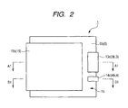
- FIG. 2 is a bottom view (base view, back side view, plan view) thereof
- FIG. 3 and FIG. 4 are sectional views (side surface sectional views) thereof.
- a section taken along line A1-A1 of FIG. 1 substantially corresponds to FIG. 3
- a section taken along line B1-B1 of FIG. 1 substantially corresponds to FIG. 4 .
- the semiconductor device (semiconductor package) 1 in this embodiment is a resin sealed and surface mounted semiconductor package. That is, the semiconductor device 1 is a semiconductor device of a resin sealed semiconductor package type.
- the semiconductor device 1 in this embodiment, illustrated in FIG. 1 to FIG. 4 includes: a semiconductor chip 2; a source terminal (terminal for source, conductor section for coupling a source, conductor section, second conductor section) 3, a gate terminal (terminal for gate, conductor section for coupling a gate, conductor section, second conductor section) 4, and a drain terminal (terminal for drain, conductor section for coupling a drain, conductor section, first conductor section) 5, each formed of a conductor; and an encapsulation resin section (sealing section, encapsulation resin) 6 sealing all of them.
- the encapsulation resin section 6 is formed of resin material, such as thermosetting resin, and may contain filler or the like.
- resin material such as thermosetting resin
- epoxy resin or the like containing filler can be used to form the encapsulation resin section 6.
- the semiconductor chip 2, source terminal 3, gate terminal 4, and drain terminal 5 are sealed and protected by the encapsulation resin section 6.
- the encapsulation resin section 6 has a top surface (front surface, second surface) 6a and a back surface (bottom surface, under surface, first surface) 6b, which are two principal surfaces positioned on the opposite side to each other.
- the back surface 6b of the encapsulation resin section 6, that is, the back surface (bottom surface, under surface) 1b of the semiconductor device 1 is the mounting surface of the semiconductor device 1.
- the semiconductor chip 2 is obtained by: forming various semiconductor elements or semiconductor integrated circuits in a semiconductor substrate (semiconductor wafer) comprised of, for example, single crystal silicon or the like; grinding the back surface of the semiconductor substrate as required; and then dividing the semiconductor substrate into individual semiconductor chips 2 by dicing or the like.
- the semiconductor chip 2 is sealed in the encapsulation resin section 6 and is not exposed from the encapsulation resin section 6.
- a semiconductor chip with a vertical power MISFET (Metal Insulator Semiconductor Field Effect Transistor) of trench gate structure formed therein can be used for the semiconductor chip 2.
- the semiconductor chip 2 has a front surface 2a and a back surface 2b, which are two principal surfaces positioned on the opposite side to each other.
- the semiconductor chip 2 includes: a source pad electrode (front surface electrode) 2s and a gate pad electrode (front surface electrode) 2g formed in the front surface 2a of the semiconductor chip 2; and a back surface drain electrode (back surface electrode) 2d formed in the entire back surface 2b of the semiconductor chip 2.
- the source pad electrode 2s is electrically coupled to the source of MISFET formed in the semiconductor chip 2; the gate pad electrode 2g is electrically coupled to the gate electrode of the MISFET formed in the semiconductor chip 2; and the back surface drain electrode 2d is electrically coupled to the drain of the MISFET formed in the semiconductor chip 2.
- FIG. 5 is a plan view (top view) illustrating an example of the chip layout of the semiconductor chip 2.
- the source pad electrode 2s and the gate pad electrode 2g are formed in the front surface 2a of the semiconductor chip 2.
- the disposition of each electrode may be modified as required.
- the source terminal 3, gate terminal 4, and drain terminal 5 are formed of conductive material, for example, metal material, such as copper (Cu) or copper alloy.
- the semiconductor chip 2 is so disposed that the following is implemented: the semiconductor chip 2 is positioned between the drain terminal 5 positioned under the semiconductor chip 2 and the source terminal 3 and the gate terminal 4 positioned above the semiconductor chip 2; and the front surface 2a of the semiconductor chip 2 surfaces upward.
- conductive bonding material (adhesive) 7 The following is implemented through conductive bonding material (adhesive) 7: the source terminal 3 is joined (bonded, coupled) with the source pad electrode 2s in the front surface 2a of the semiconductor chip 2; the gate terminal 4 is joined (bonded, coupled) with the gate pad electrode 2g in the front surface 2a of the semiconductor chip 2; and the drain terminal 5 is joined (bonded, coupled) with the back surface drain electrode 2d in the back surface 2b of the semiconductor chip 2.
- the source terminal 3 is electrically coupled to the source pad electrode 2s of the semiconductor chip 2 through the bonding material 7;
- the gate terminal 4 is electrically coupled to the gate pad electrode 2g of the semiconductor chip 2 through the bonding material 7; and the drain terminal 5 is electrically coupled to the back surface drain electrode 2d of the semiconductor chip 2 through the bonding material 7.
- the conductive bonding material 7 is preferably obtained by curing solder or silver (Ag) paste.
- the under surface 15b of the drain terminal 5 is exposed at the back surface 6b of the encapsulation resin section 6.
- a side surface (end surface, end) 15c of the drain terminal 5 is exposed at a side surface of the encapsulation resin section 6 and the other side surfaces (end surfaces, ends) of the drain terminal 5 are covered and sealed with the encapsulation resin section 6.
- the exposed side surface 15c of the drain terminal 5 is a side surface (end surface) produced as the result of a cutting step (corresponding to Step S11, describe later) during the manufacture of the semiconductor device 1.
- Part of the top surface 15a of the drain terminal 5 is joined with the back surface drain electrode 2d of the semiconductor chip 2 through the conductive bonding material 7; and the other part of the top surface 15a of the drain terminal 5 is covered and sealed with the encapsulation resin section 6.
- the source terminal 3 includes: a first portion (chip coupling portion, conductor section) 3a; a second portion (external terminal composing portion, conductor section) 3b; and a stepped portion (bent portion, coupling portion, conductor section) 3c that couples the first portion 3a and the second portion 3b together.
- the first portion 3a, second portion 3b, and stepped portion 3c are integrally formed of the same conductive material and the stepped portion 3c couples together the first portion 3a and the second portion 3b different in height from each other.
- Part of the under surface 13a of the first portion 3a of the source terminal 3 is joined to the source pad electrode 2s of the semiconductor chip 2 through the conductive bonding material 7; and the other part of the under surface 13a of the first portion 3a of the source terminal 3 is covered and sealed with the encapsulation resin section 6.
- the top surface 13b of the first portion 3a of the source terminal 3 is exposed at the top surface 6a of the encapsulation resin section 6.
- the stepped portion 3c of the source terminal 3 is covered with the encapsulation resin section 6 and sealed in the encapsulation resin section 6.
- the under surface 13c of the second portion 3b of the source terminal 3 is exposed at the back surface 6b of the encapsulation resin section 6.
- a side surface (end surface, end) 13d of the second portion 3b of the source terminal 3 is exposed at a side surface of the encapsulation resin section 6.
- the side surface 13d is an end side surface 13d on the opposite side to the side where the second portion 3b is coupled to the stepped portion 3c.
- the other side surfaces (end surfaces, ends) of the second portion 3b of the source terminal 3 are covered and sealed with the encapsulation resin section 6.
- the exposed side surface 13d of the source terminal 3 is a side surface (end surface) produced as the result of a cutting step (corresponding to Step S11, described later) during the manufacture of the semiconductor device 1.
- the gate terminal 4 includes: a first portion (chip coupling portion, conductor section) 4a; a second portion (external terminal composing portion, conductor section) 4b; and a stepped portion (bent portion, coupling portion, conductor section) 4c that couples the first portion 4a and the second portion 4b together.
- the first portion 4a, second portion 4b, and stepped portion 4c are integrally formed of the same conductive material and the stepped portion 4c couples together the first portion 4a and the second portion 4b different in height from each other.
- Part of the under surface 14a of the first portion 4a of the gate terminal 4 is joined to the gate pad electrode 2g of the semiconductor chip 2 through the conductive bonding material 7; and the other part of the under surface 14a of the first portion 4a of the gate terminal 4 is covered and sealed with the encapsulation resin section 6.
- the top surface 14b of the first portion 4a of the gate terminal 4 is exposed at the top surface 6a of the encapsulation resin section 6.
- the stepped portion 4c of the gate terminal 4 is covered with the encapsulation resin section 6 and sealed in the encapsulation resin section 6.
- the under surface 14c of the second portion 4b of the gate terminal 4 is exposed at the back surface 6b of the encapsulation resin section 6.
- a side surface (end surface, end) 14d of the second portion 4b of the gate terminal 4 is exposed at a side surface of the encapsulation resin section 6.
- the side surface 14d is an end side surface 14d on the opposite side to the side where the second portion 4b is coupled to the stepped portion 4c.
- the other side surfaces (end surfaces, ends) of the second portion 4b of the gate terminal 4 are covered and sealed with the encapsulation resin section 6.
- the exposed side surface 14d of the gate terminal 4 is a side surface (end surface) produced as the result of a cutting step (corresponding to Step S11, described later) during the manufacture of the semiconductor device 1.
- the bonding material (adhesive) 7 exists between the back surface 2b (back surface drain electrode 2d) of the semiconductor chip 2 and the top surface 15a of the drain terminal 5.
- a film member (film for bonding) 8a also exists there. Between the back surface 2b of the semiconductor chip 2 and the top surface 15a of the drain terminal 5, the bonding material 7 and the film member 8a do not overlap each other on a plane. (That is, they do not overlap each other as viewed from a plane parallel with the front surface 2a of the semiconductor chip 2.)
- the bonding material 7 is placed in an area of the back surface 2b (back surface drain electrode 2d) of the semiconductor chip 2 where the film member 8a is not placed.
- the bonding material (adhesive) 7 exists between the front surface 2a of the semiconductor chip 2 and the following under surfaces: the under surface 13a of the first portion 3a of the source terminal 3 and the under surface 14a of the first portion 4a of the gate terminal 4.
- a film member (film for bonding) 8b also exists there. Between the front surface 2a of the semiconductor chip 2 and the under surfaces 13a, 14a of the source terminal 3 and gate terminal 4, the bonding material 7 and the film member 8b do not overlap each other on a plane.
- the film member 8b is preferably placed in a position on the front surface 2a of the semiconductor chip 2 where it does not overlap the source pad electrode 2s or the gate pad electrode 2g.
- the bonding material 7 is placed on the front surface 2a of the semiconductor chip 2 over the source pad electrode 2s and the gate pad electrode 2g.
- the film member 8a and the film member 8b are preferably formed of films of substantially the same sort except that they are different in planar shape.
- the following under surfaces exposed at the back surface 6b of the encapsulation resin section 6 should be formed substantially flush with one another: the under surface 13c of the second portion 3b of the source terminal 3; the under surface 14c of the second portion 4b of the gate terminal 4; and the under surface 15b of the drain terminal 5.
- the following under surfaces are exposed at the back surface (bottom surface) 1b of the semiconductor device 1 corresponding to the back surface 6b of the encapsulation resin section 6: the under surface 13c of the second portion 3b of the source terminal 3; the under surface 14c of the second portion 4b of the gate terminal 4; and the under surface 15b of the drain terminal 5. These exposed portions function as external terminals (terminals, external coupling terminals, terminals for external coupling) of the semiconductor device 1.
- the above exposed portions include the under surface 13c of the second portion 3b of the source terminal 3, the under surface 14c of the second portion 4b of the gate terminal 4, and the under surface 15b of the drain terminal 5.
- the source terminal 3, gate terminal 4, and drain terminal 5 are exposed at the back surface 1b of the semiconductor device 1 (the back surface 6b of the encapsulation resin section 6)
- the semiconductor device 1 can be surface mounted.
- the back surface 1b of the semiconductor device 1 (the back surface 6b of the encapsulation resin section 6) functions as the mounting surface of the semiconductor device 1.
- the following top surfaces are exposed at the top surface 1a of the semiconductor device 1: the top surface 13b of the first portion 3a of the source terminal 3 and the top surface 14b of the first portion 4a of the gate terminal 4.
- the top surface 1a is, in other words, the principal surface of the semiconductor device 1 on the opposite side to the back surface 1b.
- the top surface 13b and the top surface 14b are exposed at the front surface 6a of the encapsulation resin section 6.
- the semiconductor device 1 in this embodiment is a semiconductor device of a resin sealed semiconductor package type having exposed conductors on the top and under surfaces.
- the first portion 3a of the source terminal 3 and the first portion 4a of the gate terminal 4 are exposed conductors on the top surface 1a (top surface 6a) side.
- the second portion 3b of the source terminal 3, the second portion 4b of the gate terminal 4, and the drain terminal 5 are exposed conductors on the back surface 1b (back surface 6b) side.
- the conductor sections coupled (joined) to the semiconductor chip 2 are exposed not only at the back surface 1b of the semiconductor device 1 (the back surface 6b of the encapsulation resin section 6).
- the conductor sections are also exposed at the top surface 1a of the semiconductor device 1 (the top surface 6a of the encapsulation resin section 6).
- the conductor sections include the first portion 3a of the source terminal 3 and the first portion 4a of the gate terminal 4.
- FIG. 6 is a process flowchart illustrating the manufacturing process for the semiconductor device 1 in this embodiment.
- FIG. 7 and FIG. 8 are sectional views of substantial parts of the semiconductor chip 2 in the manufacturing process.
- FIG. 9 is a plan view illustrating lead frames 21, 22.
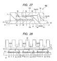
- the drawings from FIG. 10 to FIG. 27 are substantial part plan views, substantial part sectional views, or explanatory drawings illustrating the manufacturing process for the semiconductor device 1 in this embodiment.
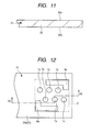
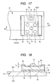
- FIG. 10 , FIG. 12 , FIG. 15 , FIG. 17 , and FIG. 19 are plan views (substantial part plan views); and FIG. 11 , FIG. 13 , FIG. 16 , FIG. 18 , and FIG.
- FIG. 20 to FIG. 27 are sectional views (substantial part sectional views).
- FIG. 10 and FIG. 11 correspond to an identical process step
- FIG. 12 and FIG. 13 correspond to an identical process step
- FIG. 15 and FIG. 16 correspond to an identical process step
- FIG. 17 and FIG. 18 correspond to an identical process step
- FIG. 19, FIG. 20 , and FIG. 21 correspond to an identical process step.
- FIG. 20 and FIG. 21 correspond to different sectional views at the identical process step
- FIG. 22 and FIG. 23 correspond to different sectional views at the identical process step.
- FIG. 27 are sectional views that substantially correspond to sections taken along line A2-A2 illustrated in FIG. 10 , FIG. 12 , FIG. 15 , FIG. 17 , and FIG. 19 and are substantially equivalent to FIG. 3 .
- the sectional views in FIG. 21 and FIG. 23 are sectional views that substantially correspond to a section taken along line B2-B2 illustrated in FIG. 19 and are substantially equivalent to FIG. 4 .
- FIG. 14 is an explanatory drawing of a preparation step for the film members 8a, 8b.
- Step S1 To manufacture the semiconductor device 1, first, the semiconductor chip 2 and the lead frames (conductive material members) 21, 22 are prepared (Step S1).
- an epitaxial layer 101b is grown over a principal surface of a semiconductor substrate (semiconductor wafer) 101a to form a semiconductor substrate (semiconductor wafer, so-called epitaxial wafer) 101 as illustrated in FIG. 7 .
- the semiconductor substrate 101a is comprised of n + -type single crystal silicon or the like implanted with, for example, arsenic (As).
- the epitaxial layer 101b is comprised of n - -type single crystal silicon.
- an insulating film silicon oxide film
- this insulating film is patterned to form an insulating film 102 (SiO 2 plate).
- a p-type impurity for example, boron (B)
- B boron
- the semiconductor substrate 101 is dry-etched to form grooves for trench gate formation, that is, trenches 104 for gate.
- the trenches 104 for gate have such dimensions that the depth thereof is larger than that of the p-type well 103 and shallower than the bottom of the epitaxial layer 101b.
- a relatively thin gate insulating film (silicon oxide film) 105 is formed over the inner wall surfaces (side surfaces and bottom surfaces) of the trenches 4 for gate and the like.
- a conductor film comprised of, for example, a low-resistance polycrystalline silicon film or the like is formed over the principal surface of the semiconductor substrate 101.
- a photoresist pattern (not shown) that covers a gate wiring formation region and does not cover the other regions is formed over the above-mentioned conductor film. Using this photoresist pattern as an etching mask, the above-mentioned conductor film is etched back to from the following sections: a gate section 106 comprised of low-resistance polycrystalline silicon or the like filled in the trenches 104 for gate and a gate wiring section 106a formed integrally with the gate section 106.
- a p-type impurity for example, boron (B)
- B boron
- n-type impurity for example, arsenic (As)
- As arsenic
- An insulating film 112 is formed over the principal surface of the semiconductor substrate 101 and is patterned by photolithography and etching. At this time, the following holes are formed in the insulating film 112: a contact hole 113 for exposing the principal surface of the semiconductor substrate 101 and a through hole 114 for exposing part of the gate wiring section 106a.
- the semiconductor substrate 101 exposed in the contact holes 113 is etched to form holes 115. Thereafter, the semiconductor substrate 101 exposed in the contact holes 113 and the holes 115 is ion-implanted with, for example, a p-type impurity (for example, boron (B)) to form a p + -type semiconductor region.
- a p-type impurity for example, boron (B)
- a titanium tungsten film (not shown) is formed over the principal surface of the semiconductor substrate 101 and then an aluminum film (or an aluminum alloy film) 116 is formed thereover by sputtering or the like. Subsequently, the laminated film of the titanium tungsten film and the aluminum film 116 is patterned by photolithography and etching. As a result, front surface electrodes, such as a gate electrode 116a and a source wiring 116b, are formed.
- An insulating film (protective film) 117 for front surface protection comprised of, for example, polyimide resin or the like is formed over the principal surface of the semiconductor substrate 101. Subsequently, using photolithography and etching, the insulating film 117 is patterned to form openings (not shown) exposing part of the gate electrode 116a and the source wiring 116b, and thus bonding pads are formed.
- the gate electrode 116a exposed in an opening in the insulating film 117 becomes the above-mentioned gate pad electrode 2g of the semiconductor chip 2; and the source wiring 116b exposed in an opening in the insulating film 117 becomes the above-mentioned source pad electrode 2s.
- the back surface of the semiconductor substrate 101 is ground or polished to reduce the thickness thereof. Thereafter, for example, nickel, titanium, or nickel and gold is deposited on the back surface of the semiconductor substrate 101 by a vapor deposition method or the like to form a drain electrode 118.
- This drain electrode 118 becomes the above-mentioned back surface drain electrode 2d of the semiconductor chip 2.
- Such a semiconductor element as a vertical power MISFET of trench gate structure is formed in the semiconductor substrate 101.
- the semiconductor substrate 101 is cut or diced using a dicing saw or the like and thereby separated into segmented semiconductor chips 2.
- the semiconductor chip 2 with the vertical power MISFET of trench gate structure formed therein is manufactured.
- the vertical MISFET corresponds to MISFET in which a source-drain current flows in the direction of the thickness of a semiconductor substrate (direction substantially perpendicular to the principal surface of the semiconductor substrate).
- Lead frames 21, 22 used in the manufacture of the semiconductor device 1 are conductive material members comprised of conductive material and are formed of metal material, such as copper (Cu) or copper alloy.
- the lead frame 21 has a drain terminal portion 25 that becomes the drain terminal 5 later and is so structured that multiple drain terminal portions 25 are integrally tied with a frame rim 21a.
- the lead frame 22 has a source terminal portion 23 that becomes the source terminal 3 later and a gate terminal portion 24 that becomes the gate terminal 4 later.
- the lead frame 22 is so structured that a source terminal portion 23 and a gate terminal portion 24 are paired with each other and multiple pairs are integrally tied with a frame rim 22a.
- Each source terminal portion 23 of the lead frame 22 includes: a first portion 23a of the source terminal portion 23 that becomes the first portion 3a of the source terminal 3 later; a second portion 23b of the source terminal portion 23 that becomes the second portion 3b of the source terminal 3 later; and a stepped portion (bent portion) 23c of the source terminal portion 23 that becomes the stepped portion (bent portion) 3c of the source terminal 3 later. These portions are integrally formed.
- Each gate terminal portion 24 of the lead frame 22 includes: a first portion 24a of the gate terminal portion 24 that becomes the first portion 4a of the gate terminal 4 later; a second portion 24b of the gate terminal portion 24 that becomes the second portion 4b of the gate terminal 4 later; and a stepped portion (bent portion) 24c of the gate terminal portion 24 that becomes the stepped portion (bent portion) 4c of the gate terminal 4 later. These portions are integrally formed.
- each source terminal portion 23 and each gate terminal portion 24 are tied with the frame rim 20b at the respective ends (ends of the second portions 23b, 24b) and are integrally formed.
- the lead frames 21, 22 are multiple lead frames and the lead frames 21, 22 can be used to manufacture multiple semiconductor devices 1 at once. At this time, one semiconductor device 1 is manufactured from one drain terminal portion 25 and one pair of a source terminal portion 23 and a gate terminal portion 24.
- the lead frames 21, 22 illustrated in FIG. 10 to FIG. 13 and FIG. 15 to FIG. 21 referred to later, correspond to areas 20a, 20b illustrated in FIG. 9 .
- the lead frames 21, 22 may be provided with perforations (not shown) along a line along which the lead frames are to be cut to facilitate cutting of the lead frames 21, 22 described later.
- the lead frames 21, 22 can be manufactured by processing a metal plate (copper plate or the like) into a desired shape by, for example, molding (pressing), etching, or the like or by other like methods.
- FIG. 10 and FIG. 11 illustrate a drain terminal portion 25 of a lead frame 21 that underwent Step S1 before Step S2, described later, is carried out.
- a film member (film for bonding) 8a is placed (mounted, stuck to) over the lead frame 21 as illustrated in FIG. 12 and FIG. 13 (Step S2). Specifically, at Step S2, the film member 8a is placed (mounted) over the first principal surface (top surface) 35a of a drain terminal portion 25 of the lead frame 21.
- the film member 8a has a thickness of T 1 .
- Each drain terminal portion 25 of the lead frame 21 has a first principal surface (top surface) 35a and a second principal surface (under surface) 35b on the opposite side to each other.
- the first principal surface 35a becomes the top surface 15a of the drain terminal 5 later and the second principal surface 35b becomes the under surface 15b of the drain terminal 5 later.
- the film member 8a is placed (mounted) in part of an area where the semiconductor chip 2 is to be mounted.
- the area where the semiconductor chip 2 is disposed later is indicated by a broken line to facilitate understanding.
- a die bonding film (die attach film) or the like can be used for the film member 8a and the film member 8b used later.
- FIG. 14 is an explanatory drawing illustrating an example of a preparation step for the film member 8a and the film member 8b described later.
- the sketch (a) in FIG. 14 illustrates the film members before cutting.
- the upper illustration in the sketch (a) in FIG. 14 is a schematic plan view (top view) and the lower illustration is a schematic sectional view though not hatched.
- the sketch (b) in FIG. 14 illustrates the film members after cutting.
- the upper illustration in the sketch (b) in FIG. 14 is a schematic plan view (top view) and the lower illustration is a schematic sectional view though not hatched.
- the film 8 is cut into a desired shape.
- the base material layer 37 is not cut.
- the cut film 8 becomes the film members 8a (or the film members 8b described later).
- a film member 8a is picked up (stripped) from the base material layer 37 and placed over the lead frame 21 at Step S2.
- Step S5 described later, a film member 8b is picked up from the base material layer 37 and placed over the semiconductor chip 2.
- Step S3 the conductive bonding material 7a is placed over the lead frame 21 as illustrated in FIG. 12 and FIG. 13 (Step S3).
- the bonding material 7a is placed over (applied to) the first principal surface 35a of each drain terminal portion 25 of the lead frame 21.
- the bonding material 7a is a paste-like bonding material and is preferably solder paste or silver paste.
- the bonding material 7a is placed in or applied to the following area of the first principal surface 35a of each drain terminal portion 25 of the lead frame 21: an area where the semiconductor chip 2 is to be mounted and the film member 8a is not placed.
- FIG. 12 and FIG. 13 illustrate a state in which the steps up to Step S3, or the bonding material 7a placement step, have been carried out.
- the semiconductor chip 2 is placed (mounted) over the lead frame 21 (Step S4).
- Step S4 specifically, the semiconductor chip 2 is placed (mounted) over the first principal surface 35a of each drain terminal portion 25 of the lead frame 21 so that the following is implemented: the front surface 2a of the semiconductor chip 2 surfaces upward; and the back surface 2b (back surface drain electrode 2d side) of the semiconductor chip 2 is opposed to the first principal surface 35a of each drain terminal portion 25 of the lead frame 21.
- the semiconductor chip 2 is placed (mounted) over the first principal surface 35a of each drain terminal portion 25 of the lead frame 21 with the bonding material 7a and the film member 8a in-between.
- the semiconductor chip 2 is temporarily fixed by the adhesion (adherence) of either or both of the bonding material 7a and the film member 8a.
- film members (films for bonding) 8b are placed over (mounted over, stuck to) the front surface 2a of the semiconductor chip 2 (Step S5).
- the film member 8b has a thickness of t 2 .
- the film member 8b is placed (mounted) over the front surface 2a of the semiconductor chip 2 in positions where they do not overlap the gate pad electrode 2g or the source pad electrode 2s.
- Conductive bonding material 7b is placed over the front surface 2a of the semiconductor chip 2 (Step S6).
- the bonding material 7b is a paste-like bonding material and is preferably solder paste or silver paste.
- the bonding material 7b is a bonding material of the same sort as the bonding material 7a. Therefore, when the bonding material 7a is silver paste, the bonding material 7b is also comprised of silver paste; and when the bonding material 7a is solder paste, the bonding material 7b is also comprised of solder paste.
- the bonding material 7b is placed or applied in an area of the front surface 2a of the semiconductor chip 2 where the film member 8b is not placed.
- FIG. 17 and FIG. 18 illustrate a state in which the steps up to Step S6, or the bonding material 7b placement step, have been carried out.
- the lead frame 22 is placed over the front surface 2a of the semiconductor chip 2 (Step S7).
- Step S7 specifically, the lead frame 22 is placed over the lead frame 21 and the semiconductor chip 2 so that the following is implemented: the first portion 23a of each source terminal portion 23 of the lead frame 22 is placed over the source pad electrode 2s of each semiconductor chip 2; and at the same time, the first portion 24a of each gate terminal portion 24 of the lead frame 22 is placed over the gate pad electrode 2g of each semiconductor chip 2.
- the following are placed (mounted) over the front surface 2a of the semiconductor chip 2 with the bonding material 7b and the film member 8b in-between: the first portion 23a of a source terminal portion 23 of the lead frame 22 (the first principal surface 33a thereof) ; and the first portion 24a of a gate terminal portion 24 (the first principal surface 34a thereof). These portions are temporarily fixed by the adhesion (adherence) of either or both of the bonding material 7b and the film member 8a.
- the first portion 23a of each source terminal portion 23 of the lead frame 22 has a first principal surface (under surface) 33a and a second principal surface (top surface) 33b on the opposite side to each other.
- the first principal surface 33a becomes the under surface 13a of the first portion 3a of the source terminal 3 later.
- the second principal surface 33b becomes the top surface 13b of the first portion 3a of the source terminal 3 later.
- the top surface 13b is a surface exposed from the top surface 6a of the encapsulation resin section 6.
- the first portion 24a of each gate terminal portion 24 of the lead frame 22 has a first principal surface (under surface) 34a and a second principal surface (top surface) 34b on the opposite side to each other.
- the first principal surface 34a becomes the under surface 14a of the first portion 4a of the gate terminal 4 later.
- the second principal surface 34b becomes the top surface 14b of the first portion 4a of the gate terminal 4.
- the top surface 14b is a surface exposed from the top surface 6a of the encapsulation resin section 6.
- FIG. 21 the area covered with the encapsulation resin section 6 later (area where the encapsulation resin 6 is to be formed) is indicated by a broken line to facilitate understanding.
- Step S8 the bonding materials 7a, 7b are cured.
- solder reflow is carried out at Step S8 to melt and solidify (re-solidify) the bonding materials 7a, 7b.
- bonding material 7a, 7b are silver paste
- heat treatment for curing the silver paste is carried out at Step S8 to cure the bonding materials 7a, 7b.
- Step S8 for the bonding materials 7a, 7b, the following are respectively joined and electrically coupled together through the bonding material 7 (the cured bonding materials 7a, 7b) as illustrated in FIG. 22 and FIG. 23 : each source terminal portion 23, gate terminal portion 24, and drain terminal portion 25 of the lead frames 21, 22 and the source pad electrode 2s, gate pad electrode 2g, and back surface drain electrode 2d of each semiconductor chip 2. More specific description will be given.
- the first portion 23a (first principal surface 33a thereof) of a source terminal portion 23 of the lead frame 22 and the source pad electrode 2s of the semiconductor chip 2 are joined and electrically coupled together through the bonding material 7.
- the first portion 24a (first principal surface 34a thereof) of a gate terminal portion 24 of the lead frame 22 and the gate pad electrode 2g of the semiconductor chip 2 are joined and electrically coupled together through the bonding material 7.
- the back surface drain electrode 2d of the semiconductor chip 2 and (the first principal surface 35a of) a drain terminal portion 25 of the lead frame 21 are joined and electrically coupled together through the bonding material 7.
- the bonding material 7 is the bonding materials 7a, 7b cured by the processing of Step S8.
- the bonding materials 7a, 7b are solder paste
- the bonding materials 7a, 7b comprised of solder paste are melted and solidified by the solder reflow at Step S8 and turned into the bonding material 7 comprised of solder.
- the bonding materials 7a, 7b are silver paste
- the bonding materials 7a, 7b comprised of silver paste are cured by the heat treatment of Step S8 and turned into the bonding material 7.
- the film members 8a, 8b are also cured.
- the cured film member 8a contributes to the junction (bonding) between the back surface 2b of the semiconductor chip 2 and the drain terminal portion 25.
- the cured film member 8b contributes to the junction (bonding) between the front surface 2a of the semiconductor chip 2 and the first portion 23a of the source terminal portion 23 and the first portion 24a of the gate terminal portion 24.
- the film members 8a, 8b can be regarded as films for bonding (film-type adhesive, film-type bonding material).
- Step S8 cleaning may be carried out to remove flux and the like as required.
- a source terminal portion 23 of the lead frame 22 is joined to the source pad electrode 2s in the front surface 2a of the semiconductor chip 2; a gate terminal portion 24 of the lead frame 22 is joined to the gate pad electrode 2g in the front surface 2a of the semiconductor chip 2; and a drain terminal portion 25 of the lead frame 21 is joined to the back surface drain electrode 2d in the back surface 2b of the semiconductor chip 2.
- an assembly (work) 40 comprised of the lead frames 21, 22 and a semiconductor chip 2 joined therebetween is obtained.
- a molding step (resin molding step, for example, transfer molding step) is carried out to form the encapsulation resin section 6 and each semiconductor chip 2 is sealed with the encapsulation resin section 6 (Step S9).
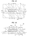
- FIG. 24 illustrates the assembly 40 fixed in a mold 41, 42 (upper die 41 and lower die 42) at the molding step, Step S9.
- Step S9 the assembly 40 is fixed in the mold 41, 42. More specific description will be given. As illustrated in FIG. 24 , the peripheral portions of the lead frames 21, 22 are sandwiched and clamped (fixed) between the dies 41, 42 so that the following is implemented: each source terminal portion 23 and gate terminal portion 24 of the lead frame 22, each drain terminal portion 25 of the lead frame 21, and each semiconductor chip 2 therebetween are disposed in a cavity 43. This cavity is formed by the under surface 41a of the die 41 and the top surface 42a of the die 42.
- the second principal surface (under surface) 35b of each drain terminal portion 25 of the lead frame 21 is a surface on the opposite side to the side where it is opposed to the back surface 2b of the semiconductor chip 2. That is, the second principal surface (under surface) 35b of the drain terminal portion 25 of the lead frame 21 is a surface on the opposite side to the side where it is joined to the back surface drain electrode 2d.
- the second principal surface (under surface) 35b becomes the under surface 15b of the drain terminal 5.
- the under surface 33c of the second portion 23b of each source terminal portion 23 of the lead frame 22 becomes the following: the under surface 13c of the second portion 3b of the source terminal 3.
- the under surface 34c of the second portion 24b of each gate terminal portion 24 of the lead frame 22 becomes the following: the under surface 14c of the second portion 4b of the gate terminal 4.
- the second principal surface (top surface) 33b of the first portion 23a of each source terminal portion 23 of the lead frame 22 becomes the following: the top surface 13b of the first portion 3a of the source terminal 3.
- the second principal surface (top surface) 34b of the first portion 24a of each gate terminal portion 24 of the lead frame 22 becomes the following: the top surface 14b of the first portion 4a of the gate terminal 4.
- the height h 1 of the assembly 40 immediately before the molding step is equivalent to the height (distance) from the second principal surface (under surface) 35b of the drain terminal portion 25 to the following: the second principal surface (top surface) 33b of the first portion 23a of the source terminal portion 23 and the second principal surface (top surface) 34b of the first portion 24a of the gate terminal portion 24.
- the height h 0 of the cavity 43 in the mold 41, 42 is equivalent to the distance from the under surface 41a of the die 41 to the top surface 42a of the die 42 in the cavity 43 when the dies 41, 42 are clamped together.
- the lead frames 21, 22 are clamped and fixed between the dies 41, 42 as illustrated in FIG. 24 . Thereafter, encapsulation resin material 46 as the material for the formation of the encapsulation resin section 6 is injected (guided, filled) into the cavity 43 in the mold 41, 42 as illustrated in FIG. 25 . The injected encapsulation resin material 46 is cured to form the encapsulation resin section 6.
- the encapsulation resin material 46 for the formation of the encapsulation resin section 6 is comprised of resin material, such as thermosetting resin material, or the like.
- the encapsulation resin material may contain filler or the like and, for example, epoxy resin containing filler and the like can be used as the encapsulation resin material.
- the encapsulation resin material 46 is comprised of thermosetting resin material
- the encapsulation resin material 46 is injected into the cavity 43 in the mold 41, 42 and then the dies 41, 42 are heated to a predetermined temperature.
- the encapsulation resin material 46 can be thereby heated and cured.
- the bonding material 7 is solder
- it is desirable that the temperature at which the encapsulation resin material 46 is cured should be lower than the melting point of the solder composing the bonding material 7. As a result, it is possible to prevent the solder from being melted while the encapsulation resin material 46 is being cured.
- the encapsulation resin section 6 is formed.
- the following measure may be taken: the work and the mold in FIG. 24 and FIG. 25 are turned upside down and the lead frames 21, 22 and the semiconductor chip 2 are set in the dies 41, 42 so that the back surface drain electrode 2d of the semiconductor chip 2 faces upward.
- the die 41 is lower die and the die 42 is upper die.
- the assembly 40 with the encapsulation resin section 6 formed thereon (that is, an assembly 40a) is released from the dies 41, 42.
- the molding step, Step S9, is carried out as mentioned above.
- fins and the like are removed from the encapsulation resin section 6 as required.
- the assembly 40a is the assembly 40 with the encapsulation resin section 6 formed thereon.
- the formed encapsulation resin section 6 has a top surface 6a and a back surface 6b which are two principal surfaces positioned on the opposite side to each other.
- the encapsulation resin section 6 seals the semiconductor chip 2, source terminal portion 23, gate terminal portion 24, and drain terminal portion 25.
- Step S9 there is substantially no gap between the following and the top surface 42a of the die 42: the second principal surface (under surface) 35b of each drain terminal portion 25 of the lead frame 21; the under surface 34c of the second portion 24b of each gate terminal portion 24 of the lead frame 22; and the under surface 33c of the second portion 23b of each source terminal portion 23 of the lead frame 22. Therefore, the encapsulation resin section 6 is hardly formed thereon.
- Step S9 there is substantially no gap between the following and the under surface 41a of the die 41: the second principal surface (top surface) 33b of the first portion 23a of each source terminal portion 23 of the lead frame 22; and the second principal surface (top surface) 34b of the first portion 24a of each gate terminal portion 24 of the lead frame 22. Therefore, the encapsulation resin section 6 is hardly formed thereon.
- the following are exposed from the back surface 6b of the encapsulation resin section 6: the second principal surface (under surface) 35b of the drain terminal portion 25 of the lead frame 21; the under surface 34c of the second portion 24b of the gate terminal portion 24 of the lead frame 22; and the under surface 33c of the second portion 23b of the source terminal portion 23 of the lead frame 22. Further, the following are exposed from the top surface 6a of the encapsulation resin section 6: the second principal surface (top surface) 33b of the first portion 23a of the source terminal portion 23 of the lead frame 22; and the second principal surface (top surface) 34b of the first portion 24a of the gate terminal portion 24 of the lead frame 22.
- a fin of the encapsulation resin section 6 is formed on the surface (33b, 33c, 34b, 34c, 35b) of each terminal portion to be exposed from the top surface 6a or the back surface 6b of the encapsulation resin section 6, they can be removed at the fin removal step subsequent to the molding step.
- the encapsulation resin section 6 has the conductor sections (source terminal portion 23, gate terminal portion 24, and drain terminal portion 25) exposed at the top surface 6a and the back surface 6b.
- Plating is carried out as required to form a metal skin (not shown) over the portions (portions comprised of conductive material) of the lead frames 21, 22 exposed from the encapsulation resin section 6 (Step S10).
- lead-free solder can be used to carry out solder plating or the like.
- the lead frames 21, 22 are cut in predetermined positions (Step S11). For example, the lead frames 21, 22 are cut along the cutting plane lines 47 indicated by broken lines in FIG. 26 and FIG. 27 to remove the lead frames 21, 22 protruded from the encapsulation resin section 6. Thus the individually divided semiconductor device 1 illustrated in FIG. 1 to FIG. 4 is obtained (manufactured). The semiconductor device 1 is manufactured as mentioned above.
- the source terminal portion 23 cut and separated from the lead frame 22 becomes the source terminal 3 of the semiconductor device 1; the gate terminal portion 24 cut and separated from the lead frame 22 becomes the gate terminal 4 of the semiconductor device 1; and the drain terminal portion 25 cut and separated from the lead frame 21 becomes the drain terminal 5 of the semiconductor device 1.
- the first portion 23a of the source terminal portion 23 becomes the first portion 3a of the source terminal 3; the second portion 23b of the source terminal portion 23 becomes the second portion 3b of the source terminal 3; and the stepped portion 23c of the source terminal portion 23 becomes the stepped portion 3c of the source terminal 3.
- the first portion 24a of the gate terminal portion 24 becomes the first portion 4a of the gate terminal 4; the second portion 24b of the gate terminal portion 24 becomes the second portion 4b of the gate terminal 4; and the stepped portion 24c of the gate terminal portion 24 becomes the stepped portion 4c of the gate terminal 4.
- the second principal surface (top surface) 33b of the first portion 23a of the source terminal portion 23 becomes the top surface 13b of the first portion 3a of the source terminal 3 exposed from the top surface 6a of the encapsulation resin 6; and the second principal surface (top surface) 34b of the first portion 24a of the gate terminal portion 24 becomes the top surface 14b of the first portion 4a of the gate terminal 4 exposed from the top surface 6a of the encapsulation resin 6.
- the second principal surface (under surface) 35b of the drain terminal portion 25 becomes the under surface 15b of the drain terminal 3 exposed from the back surface 6b of the encapsulation resin 6.
- the under surface 33c of the second portion 23b of the source terminal portion 23 becomes the under surface 13c of the second portion 3b of the source terminal 3 exposed from the back surface 6b of the encapsulation resin section 6; and the under surface 34c of the second portion 24b of the gate terminal portion 24 becomes the under surface 14c of the second portion 4b of the gate terminal 4 exposed from the back surface 6b of the encapsulation resin section 6.
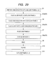
- FIG. 28 is a side view (sectional view) illustrating multiple semiconductor devices 1 mounted over a mounting board 51.
- each semiconductor device 1 is mounted over the mounting board (wiring board) 51.
- the back surface (bottom surface) 1b of each semiconductor device 1 functions as the mounting surface when it is mounted over the mounting board 51.
- the external coupling terminals exposed at the back surface 1b of each semiconductor device 1 are joined and electrically coupled with terminals 52 of the mounting board 51 through conductive bonding material 53, such as solder.
- These external coupling terminals are the source terminal 3, gate terminal 4, and drain terminal 5 (the respective under surfaces 13c, 14c, 15b thereof).
- each source terminal 3 (under surface 13c of the second portion 3b thereof) and each drain terminal 5 (under surface 15b thereof)exposed at the back surface 1b of each semiconductor device 1 are joined to terminals 52 of the mounting board 51 through the bonding material 53.
- each gate terminal 4 (under surface 14c of the second portion 4b thereof) exposed at the back surface 1b of the semiconductor device 1 is joined to a terminal 52 of the mounting board 51 through the bonding material 53.
- the radiation fin 55 is a heat radiating member formed of, for example, such metal material as aluminum (A1) or aluminum alloy.
- the heat conduction sheet 54 is an elastic insulating sheet and is relatively high in thermal conductivity.
- the heat conduction sheet 54 is formed of, for example, silicon, acrylic, or ethylene-propylene material and is comprised of a rubber-like or gel-like sheet or the like.
- the heat conduction sheet 54 may be formed of a material obtained by mixing the above materials with glass cloth as base material.
- the heat conduction sheet 54 can be sandwiched between the semiconductor devices 1 and the radiation fin 55 as a heat radiation part and caused to function to enhance the heat radiation effect.
- the radiation fin 55 is fixed over the mounting board 51 by screws, fixing brackets (not shown), or the like.
- heat-radiating resin adhesive or the like may be used to join and fix the radiation fin 55 with and on the top surfaces 1a of the semiconductor devices 1.
- each semiconductor device 1 When each semiconductor device 1 is actuated to operate the semiconductor chip 2 in the semiconductor device 1, the semiconductor chip 2 in the semiconductor device 1 produces heat.
- the semiconductor chip 2 is coupled with the source terminal 3, gate terminal 4, and drain terminal 5.
- the source terminal 3, gate terminal 4, and drain terminal 5 are formed of a conductive material (such metal as copper alloy) higher in thermal conductivity than the encapsulation resin section 6. For this reason, heat produced in the semiconductor chip 2 in each semiconductor device 1 is radiated to outside the semiconductor device 1 through the source terminal 3, gate terminal 4, and drain terminal 5. At this time, heat from each semiconductor chip 2 is radiated to the mounting board 51 through the source terminal 3, gate terminal 4, and drain terminal 5. At the same time, the heat is radiated to the radiation fin 55 through the source terminal 3, gate terminal 4, and heat conduction sheet 54.
- the radiation fin 55 has multiple fins formed therein and heat conducted from each semiconductor device 1 to the radiation fin 55 is further radiated to the outside air.
- the following are exposed as external coupling terminals at the back surface 1b of the semiconductor device 1: the source terminal 3 (second portion 3b thereof); the gate terminal 4 (second portion 4b thereof); and the drain terminal 5.
- the following are exposed at the top surface 1a of the semiconductor device 1 (the top surface 6a of the encapsulation resin section 6): the top surface 13b of the first portion 3a of the source terminal 3; and the top surface 14b of the first portion 4a of the gate terminal 4.
- the heat can be radiated from the side of the back surface 1b and the side of the top surface 1a of the semiconductor device.
- the top surface side there are the first portion 3a of the source terminal 3 and the first portion 4a of the gate terminal 4.
- the height h 1 of the assembly 40 is excessively larger than the height h 0 of the cavity 43 in the mold 41, 42 when the assembly 40 is clamped between the dies 41, 42, the following takes place: pressure from the dies 41, 42 is applied to the semiconductor chip 2 from above and below through the following: the first portion 23a of the source terminal portion 23 and the first portion 24a of the gate terminal portion 24 positioned above the semiconductor chip 2 and the drain terminal portion 25 positioned below the semiconductor chip 2.
- the portions of the source terminal portion 23, gate terminal portion 24, and drain terminal portion 25 to be exposed from the encapsulation resin 6 are covered with the encapsulation resin section 6 and are not exposed.
- Variation in the height h 1 of the assembly 40 immediately before the molding step is caused by the following: variation in the state of the junction between the semiconductor chip 2 and the lead frames 21, 22, variation in the quantity of bonding material, or the like.
- a large quantity of bonding material increases the thickness of the bonding material layers between the semiconductor chip 2 and the lead frames 21, 22.
- the height h 1 of the assembly 40 is increased.
- a small quantity of bonding material reduces the thickness of the bonding material layers between the semiconductor chip 2 and the lead frames 21, 22.
- the height h 1 of the assembly 40 is reduced.
- the height of the finished semiconductor device is defined by the height h 1 of the assembly 40 immediately before the molding step. Therefore, if there is variation in the height h 1 of the assembly 40 immediately before the molding step, the height of the finished semiconductor device varies. If there is variation in the height of the semiconductor device 1, a problem can arise in the following cases: cases where multiple semiconductor devices 1 are mounted over a mounting board 51 and a radiation fin 55 is mounted over the semiconductor devices 1 with a heat conduction sheet 54 in-between as illustrated in FIG. 28 . Variation is produced in the state of coupling between the radiation fin 55 and the semiconductor devices 1 through the heat conduction sheet 54. As a result, there is a possibility that the state of heat radiation varies from semiconductor device 1 to semiconductor device 1.
- Steps S2 to S4 the semiconductor chip 2 is placed (mounted) over the first principal surface 35a of each drain terminal portion 25 of the lead frame 21 with the film member 8a and the bonding material 7a in-between. Further, at Steps S5 to S7, the following are placed (mounted) over the front surface 2a of the semiconductor chip 2 with the film member 8a and the bonding material 7b in-between: the first portion 23a of a source terminal portion 23 and the first portion 24a of a gate terminal portion 24 of the lead frame 22.
- Step S8 for the bonding materials 7a, 7b: not only the bonding material 7a but also the film member 8a exists between the back surface 2b of the semiconductor chip 2 and the first principal surface 35a of each drain terminal portion 25 of the lead frame 21.
- the bonding material 7b but also the film member 8b exist between the following surfaces: the front surface 2a of the semiconductor chip 2; and the first principal surface 33a of the first portion 23a of each source terminal portion 23 and the first principal surface 34a of the first portion 24a of each gate terminal portion 24 of the lead frame 22.
- the film members 8a, 8b If there is not provided the film members 8a, 8b, unlike this embodiment, the following is caused by variation in the quantity of the bonding materials 7a, 7b supplied or the like as described above: after the bonding materials 7a, 7b are cured at Step S8, there is variation in the height h 1 of the assembly 40.
- the film member 8a exists between the semiconductor chip 2 and each drain terminal portion 25 of the lead frame 21.
- the film member 8a defines the distance (length) D 1 between the first principal surface (top surface) 35a of each drain terminal portion 25 of the lead frame 21 and the back surface 2b of the semiconductor chip 2.
- the film member 8b exists between the semiconductor chip 2 and each source terminal portion 23 and gate terminal portion 24 of the lead frame 22.
- the film member 8b defines the distance length) D 2 between the front surface 2a of the semiconductor chip 2 and the following: the first principal surface (under surface) 33a of the first portion 23a of each source terminal portion 23 and the first principal surface (under surface) 34a of the first portion 24a of each gate terminal portion 24 of the lead frame 22.
- the film members 8a, 8b are film-like members and thus the thicknesses T 1 T 2 thereof are easy to control.
- the film members 8a, 8b having desired thicknesses T 1 , T 2 can be obtained by, for example, cutting a film 8 having a desired thickness into a predetermined shape (shape of the film members 8a, 8b) as illustrated in FIG. 14 . For this reason, it is possible to prevent variation in the thicknesses T 1 , T 2 of the film members 8a, 8b.
- the film member 8a exists between the semiconductor chip 2 and each the drain terminal portion 25 of the lead frame 21.
- the film member 8a functions to keep the distance D 1 between the back surface 2b of the semiconductor chip 2 and each drain terminal portion 25 of the lead frame 21 substantially constant until the bonding materials 7a, 7b are cured at Step S8.
- the film member 8b exists between the semiconductor chip 2 and each source terminal portion 23 and gate terminal portion 24 of the lead frame 22.
- the film member 8b functions to keep the following distance substantially constant until the bonding materials 7a, 7b are cured at Step S8: the distance D 2 between the front surface 2a of the semiconductor chip 2 and the first portion 23a of each source terminal portion 23 and the first portion 24a of each gate terminal portion 24 of the lead frame 22.
- the bonding material 7 obtained by curing the bonding material 7a is so formed that the following is implemented: the bonding material 7 is in contact with the back surface drain electrode 2d of the semiconductor chip 2 and a drain terminal portion 25 of the lead frame 21 and joins them together.
- the film thickness thereof is defined by the film thickness of the film member 8a, not by the quantity of the supplied bonding material 7a.
- the bonding material 7 obtained by curing the bonding material 7b is so formed that it is in contact with the following: the source pad electrode 2s and gate pad electrode 2g of the semiconductor chip 2 and the first portion 23a of each source terminal portion 23 and the first portion 24a of each gate terminal portion 24 of the lead frame 22.
- the bonding material 7 joins them together.
- the film thickness thereof is defined by the film thickness of the film member 8b, not by the quantity of the supplied bonding material 7b. Fluctuation in the quantities of the supplied bonding materials 7a, 7b can be absorbed by variation in the planar size (area) of the bonding material 7. For this reason, the film thickness of the bonding material 7 can be controlled to a predetermined value by adjusting the film thickness of each of the film members 8a, 8b. Therefore, use of the film members 8a, 8b having predetermined film thicknesses makes it possible to suppress variation (fluctuation) in the film thickness of the bonding material 7. Thus it is possible to suppress variation (fluctuation) in the height h 1 of the assembly 40 immediately before the molding step.
- the film members 8a, 8b should be less prone to be deformed under load (load in the direction of thickness) as compared with the bonding materials 7a, 7b. That is, it is required that the film members 8a, 8b should be low in the ratio of deformation (ratio of deformation in the direction of thickness) under load (load in the direction of thickness) as compared with the bonding materials 7a, 7b. This means the following: when the bonding materials 7a, 7b and the film members 8a, 8b are placed on a plane and the same load is applied to them, the film members 8a, 8b are less prone to be deformed than the bonding materials 7a, 7b.
- the film members 8a, 8b are less prone to be deformed in the direction of thickness perpendicular to the above plane.
- the film members 8a, 8b are film-like members, they are less prone to be deformed under load (lower in ratio of deformation) as compared with the paste-like bonding materials 7a, 7b.
- the above distances D 1 , D 2 can be kept substantially constant by placing not only the bonding materials 7a, 7b but also the film members 8a, 8b between the semiconductor chip 2 and the terminals.
- the film members 8a, 8b should have elasticity. This brings about the effect that thermal stress in the semiconductor device is absorbed and cracking in the semiconductor chip 2 and fatigue breakdown of the bonding material 7 can be more appropriately prevented. Therefore, it is desirable that a material higher in elasticity than the bonding materials 7a, 7b should be used for the film members 8a, 8b.
- the film members 8a, 8b a material that does not deform in the direction of thickness during the heat treatment or reflow processing at the curing step, Step S8, for the bonding materials 7a, 7b; the thicknesses T 1 , T 2 thereof can be maintained as much as possible; and the above distances D 1 , D 2 can be kept at predetermined values as much as possible.
- examples of materials desirable for the film members 8a, 8b include: a material obtained by mixing spacer particles in a base film (base material layer) comprised of resin material (polyimide, epoxy resin, or the like). That is, the film members 8a, 8b are formed of a resin film (base film) with spacer particles mixed therein.
- a material that is hardly deformed by heating during the curing step, Step S8, is desirable and it is desirable that the shape of the material should be spherical.
- Metal particles are more desirable as the spacer particles; however, any other particles obtained by curing thermosetting resin particles beforehand or the like can be used as the spacer particles.
- the diameter of the spacer particles in the film member 8a should be substantially the same as the thickness T 1 of the film member 8a.
- the diameter of the spacer particles in the film member 8b should be substantially the same as the thickness T 2 of the film member 8b.
- a resin film does not contain a spacer particle, it can be used for the film members 8a, 8b as long as it is less prone to be deformed (shrunken) in the direction of thickness at the following step: the curing step (heat treatment or reflowing), Step S8, for the bonding materials 7a, 7b.
- Both a conductive film member and an insulating film member can be used as the film members 8a, 8b.
- a conductive film member is used as the film member 8a, not only the bonding material 7 but also the film member 8a can contribute to the electrical coupling between the electrodes of the semiconductor chip 2 and the terminals. Therefore, coupling resistance can be reduced more.
- the electrodes of the semiconductor chip 2 could be joined with the source terminal 3, gate terminal 4, and drain terminal 5 only by a conductive film member without use of the bonding material 7 (7a, 7b) unlike this embodiment. In this case, however, a problem arises.
- the resistance between the electrodes of the semiconductor chip 2 and the source terminal 3, gate terminal 4, and drain terminal 5 is increased as compared with cases where a bonding material 7 high in electrical conductivity, comprised of silver paste, solder, or the like. As a result, the performance of the semiconductor device is degraded.
- a semiconductor chip with a vertical power MISFET of trench gate structure formed therein is used as the semiconductor chip 2
- the passed current is large. Therefore, it is required to reduce the resistance between the electrodes of the semiconductor chip 2 and the source terminal 3, gate terminal 4, and drain terminal 5 as much as possible.
- the bonding material 7 (7a, 7b) is used to join together the electrodes of the semiconductor chip 2 and the source terminal 3, gate terminal 4, and drain terminal 5.
- a material higher in electrical conductivity (lower in electric resistivity) than the film members 8a, 8b can be used as the bonding material 7 (7a, 7b). Therefore, it is possible to reduce the resistance between the electrodes of the semiconductor chip 2 and the source terminal 3, gate terminal 4, and drain terminal 5 and thus enhance the performance of the semiconductor device 1.
- the bonding material 7 should be higher in electrical conductivity (that is, lower in electric resistivity) than the film members 8a, 8b. In other words, it is desirable that the bonding material 7 should be lower in resistance per unit area than the film members 8a, 8b.
- the unit area is a unit area on a plane parallel with the front surface 2a or the back surface 2b of the semiconductor chip 2.
- the film member 8a placed between the semiconductor chip 2 and the drain terminal 5 (drain terminal portion 25) it is desirable that the following measure should be taken as seen from FIG. 12 : the film member 8a is placed in the peripheral portion of the back surface 2b of the semiconductor chip 2, not in the central portion of the back surface 2b of the semiconductor chip 2 as viewed on a plane. (This plane is a plane parallel with the back surface 2b of the semiconductor chip 2.) As a result, it is possible to hold mainly the bonding material 7, high in electrical conductivity and adhesion, responsible for the following: the junction between the back surface drain electrode 2d of the semiconductor chip 2 and the drain terminal 5 (drain terminal portion 25).
- the bonding material 7a and at least one film member 8a are placed between the semiconductor chip 2 and the drain terminal 5 (drain terminal portion 25).
- multiple film members 8a should be placed on the back surface 2b (preferably, the peripheral portion of the back surface 2b) of the semiconductor chip 2.
- two film members 8a are placed.
- the film members 8a are placed in positions in the direction of a diagonal line of or positions along the two opposite sides of the back surface 2b of the semiconductor chip 2. This makes it possible to enhance the parallelism between the top surface 15a (first principal surface 35a) of the drain terminal 5 (drain terminal portion 25) and the back surface 2b of the semiconductor chip 2.
- the two film members 8a in FIG. 12 could be coupled together to form one film member in a planar ring shape. In this case, however, an escape route for the bonding material 7a is eliminated if a too large quantity of the bonding material 7a is supplied. Therefore, it is required to relatively accurately adjust the quantity of the supplied bonding material 7a.
- the film member 8a is divided into multiple pieces and these pieces are placed in the peripheral portion of the back surface 2b of the semiconductor chip 2 as illustrated in FIG. 12 , the following advantage is brought: even though a too large quantity of the bonding material 7a is supplied, the bonding material 7a can escape to the peripheral side when the semiconductor chip 2 is mounted at Step S4; and thus the above distance D 1 can be made identical with the thickness T 1 of the film member 8a. For this reason, it is possible to ensure a margin of the quantity of the supplied bonding material 7a.
- the film member 8b placed between the semiconductor chip 2 and the source terminal 3 (source terminal portion 23) and gate terminal 4 (gate terminal portion 24) it is desirable that the following measure should be taken as seen from FIG. 17 : the film member 8b is placed (mounted) in a position on the front surface 2a of the semiconductor chip 2 where it does not overlap the gate pad electrode 2g or the source pad electrode 2s. As a result, it is possible to appropriately place the bonding material 7b on the gate pad electrode 2g and the source pad electrode 2s at Step S6.
- the bonding material 7b and at least one film member 8b are placed between the semiconductor chip 2 and the source terminal 3 (source terminal portion 23) and gate terminal 4 (gate terminal portion 24).
- the multiple film members 8b should be placed on the front surface 2a (preferably, the peripheral portion of the front surface 2a) of the semiconductor chip 2.
- two film members 8b are placed.
- the film members 8b are placed in positions in the direction of a diagonal line of or positions along the two opposite sides of the front surface 2a of the semiconductor chip 2.
- the heights of the finished semiconductor devices 1 can be equalized, the following can be implemented when a member for heat radiation (for example, the above-mentioned radiation fin 55) is mounted over multiple semiconductor devices 1: the state of coupling between each semiconductor device 1 and the member for heat radiation becomes even and thus the state of heat radiation in each semiconductor device 1 can be made even. Therefore, it is possible to make the heat radiation characteristic of each semiconductor device uniform and enhance the performance thereof.
- a member for heat radiation for example, the above-mentioned radiation fin 55
- the semiconductor device 1 of a resin sealed semiconductor package type with the terminals exposed at the top and under surfaces is manufactured so that the following is implemented: the semiconductor chip 2 is sandwiched from above and below by the multiple terminals (source terminal 3, gate terminal 4, and drain terminal 5).
- a semiconductor chip having an electrode at only either of the front surface 2a and the back surface 2b could be used as the semiconductor chip 2.
- the great effect can be obtained when this embodiment is applied to a case where a semiconductor chip having an electrode at both the front surface 2a and the back surface 2b is used as the semiconductor chip 2.
- a semiconductor chip has a front surface electrode and a back surface electrode.
- semiconductor chips with various semiconductor elements formed therein can be used as the semiconductor chip 2 in this embodiment.
- the semiconductor chip need not be the above-mentioned semiconductor chip with a vertical power MISFET (Metal Insulator Semiconductor Field Effect Transistor) of trench gate structure formed therein and any other type of semiconductor chip can be used.
- MISFET Metal Insulator Semiconductor Field Effect Transistor
- the great effect can be obtained when this embodiment is applied to the following case: a case where a semiconductor chip producing a large amount of heat, for example, a semiconductor chip with such a power transistor as a power MISFET formed therein is used as the semiconductor chip 2.
- the semiconductor chip producing a large amount of heat is a semiconductor chip with a semiconductor amplifying element for power amplification formed therein.
- the semiconductor device 1 in this embodiment has the radiation performance thereof enhanced by exposing terminals at the top and under surfaces.
- the above-mentioned semiconductor chip with a vertical power MISFET of trench gate structure formed therein produces a relatively large amount of heat when it operates. Therefore, the greater effect can be obtained when this embodiment is applied to a case where a semiconductor chip with a vertical power MISFET of trench gate structure formed therein is used as the semiconductor chip 2. This is the same with the second to seventh embodiments described below.
- variation in the height h 1 of the assembly 40 immediately before the molding step is suppressed by taking the following measure: not only the bonding materials 7a, 7b (7) but also the film members 8a, 8b are placed between the semiconductor chip 2 and the terminals.
- variation in the height h 1 of the assembly immediately before the molding step is suppressed without use of the film member 8a or 8b. This is done by giving a twist to the type of the bonding materials 7a, 7b and the curing step for the bonding materials 7a, 7b.
- FIG. 29 is a process flowchart illustrating the manufacturing process for the semiconductor device 1c in this embodiment.
- FIG. 30, FIG. 31 , and FIG. 34 to FIG. 37 are substantial part sectional views illustrating the manufacturing process for the semiconductor device 1c in this embodiment.
- FIG. 30 and FIG. 31 are different sectional views illustrating an identical process step
- FIG. 34 and FIG. 35 are different sectional views illustrating an identical process step
- FIG. 36 and FIG. 37 are different sectional views illustrating an identical process step.
- FIG. 30 corresponds to a cross section in the same position at the same process step as in FIG. 20 in relation to the first embodiment
- FIG. 31 substantially corresponds to a cross section in the same position at the same process step as in FIG. 21 in relation to the first embodiment;
- FIG. 34 substantially corresponds to a cross section in the same position at the same process step as in FIG. 22 in relation to the first embodiment; and FIG. 35 substantially corresponds to a cross section in the same position at the same process step as in FIG. 23 in relation to the first embodiment.
- FIG. 36 is a sectional view corresponding to FIG. 3 in relation to the first embodiment and
- FIG. 37 is a sectional view corresponding to FIG. 4 in relation to the first embodiment.
- FIG. 32 and FIG. 33 are explanatory drawings of the curing step for silver paste 7c. Of these drawings, FIG. 32 is a plan view and FIG. 33 is a sectional view. FIG. 33 illustrates a cross section corresponding to that in FIG. 30 .
- Step S7 the steps up to Step S7 (lead frame 22 placement step) are carried out as in the first embodiment, except that: neither Step S2 nor S5 (film member 8a, 8b placement step) is carried out; and silver paste 7c is used as the bonding materials 7a, 7b at Steps S3 and S6 (bonding material 7a, 7b placement steps). (That is, Steps S3a and S6a are carried out in place of Steps S3 and S6.) As a result, the structure illustrated in FIG. 30 and FIG. 31 equivalent to FIG. 20 and FIG. 21 in relation to the first embodiment is obtained.
- Step S1 the semiconductor chip 2 and the lead frames 21, 22 are prepared as in the first embodiment.
- the structure and the manufacturing method of the semiconductor chip 2 and the lead frames 21, 22 are the same as in the first embodiment.
- Step S2 film member 8a placement step
- Step S3a silver paste 7c placement step
- Step S3a silver paste 7c placement step
- the silver paste 7c is placed or applied in an area in the first principal surface 35a of each drain terminal portion 25 of the lead frame 21 where the semiconductor chip 2 is to be mounted.
- the silver paste 7c contains spacer particles (spacer particles 66 described later), which will be described in detail later.
- Step S4 the semiconductor chip 2 is placed (mounted) over each drain terminal portion 25 of the lead frame 21 as in the first embodiment.
- the method for placing the semiconductor chip 2 over each drain terminal portion 25 of the lead frame 21 is the same as in the first embodiment.
- the semiconductor chip 2 is placed (mounted) over the first principal surface 35a of each drain terminal portion 25 of the lead frame 21 with the silver paste 7c in-between and is temporarily fixed by the adhesion (adherence) of the silver paste 7c.
- Step S2 film member 8a placement step
- Step S2 film member 8a placement step
- Step S5 film member 8b placement step
- silver (Ag) paste 7c second silver paste
- Step S6a silver paste 7c placement step
- Step S6a silver paste 7c placement step
- the lead frame 22 is placed over the front surface 2a of each semiconductor chip 2 as in the first embodiment.
- the method for placing the lead frame 22 over the front surface 2a of each semiconductor chip 2 is the same as in the first embodiment.
- the first portion 23a of each source terminal portion 23 of the lead frame 22 is placed over the source pad electrode 2s of each semiconductor chip 2 with the silver paste 7c in-between.
- the first portion 24a of each gate terminal portion 24 of the lead frame 22 is placed over the gate pad electrode 2g of each semiconductor chip 2 with the silver paste 7c in-between. They are temporarily fixed by the adhesion (adherence) of the silver paste 7c.
- the temporary assembly 40b is comprised of the lead frames 21, 22 and the semiconductor chip 2 sandwiched therebetween through the silver paste 7c; however, the silver paste 7c has not been cured yet.
- Steps S2 and S5 are omitted. Therefore, only the silver paste 7c exists between the following surfaces in the temporary assembly 40b: the back surface 2b (back surface drain electrode 2d) of the semiconductor chip 2 and the first principal surface (top surface) 35a of each drain terminal portion 25 of the lead frame 21.
- the temporary assembly 40b only the silver paste 7c exists between the front surface 2a of the semiconductor chip 2 and the following: the first principal surface 33a of the first portion 23a of each source terminal portion 23 and the first principal surface 34a of the first portion 24a of each gate terminal portion 24 of the lead frame 22.
- Step S8a The silver paste 7c is cured (Step S8a).
- Step S8a silver paste 7c curing step
- Step S8a bonding material 7a, 7b curing step mentioned above.
- the silver paste 7c is cured by heat treatment (heating).
- This embodiment is characterized in that the curing processing for (heat treatment for curing) the silver paste 7c is carried out while the following operation is performed at the curing step, Step S8a, for the silver paste 7c: pressure (load) is applied to each drain terminal portion 25 of the lead frame 21 and each source terminal portion 23 and gate terminal portion 24 of the lead frame 22 with the semiconductor chip 2 sandwiched therebetween.
- pressure (load) is schematically indicated by an arrow 67 and the direction of the arrow 67 is equivalent to the direction of the application of pressure (load).
- FIG. 32 and FIG. 33 are explanatory drawings illustrating an example of the curing step for the silver paste 7c.
- FIG. 32 illustrates the way the temporary assembly 40b is set over the base portion 61 of a retaining jig 60 (with the lid portion 62 removed) in the form of plan view.
- FIG. 33 illustrates the way, after the temporary assembly 40b is set over the base portion 61 of the retaining jig 60, the lid portion 62 of the retaining jig 60 is attached to the base portion 61 in the form of sectional view.
- the position in which the section in the FIG. 33 is taken corresponds to line C1-C1 of FIG. 32 .
- the temporary assembly 40b is set over the base portion 61 of the retaining jig 60 as illustrated in FIG. 32 and FIG. 33 . Then the lid portion 62 of the retaining jig 60 is attached to the base portion 61.
- the base portion 61 is provided with multiple prop-like height fixing pins 61a.
- the lid portion 62 is fixed on the base portion 61 by fitting the protrusions (projected portions) 62a of the lid portion 62 in the holes 61b provided in the tops of the height fixing pins 61a.
- the second principal surface (under surface) 35b of each drain terminal portion 25 of the lead frame 21 is brought into contact with the top surface 61c of the base portion 61 of the retaining jig 60; and the following are brought into contact with the under surface 62c of the lid portion 62 of the retaining jig 60: the second principal surface (top surface) 33b of the first portion 23a of each source terminal portion 23 and the second principal surface (top surface) 34b of the first portion 24a of each gate terminal portion 24 of the lead frame 22.
- pressure (load) is applied to the area between the following surfaces: the second principal surface (top surface) 33b of the first portion 23a of each source terminal portion 23 and the second principal surface (top surface) 34b of the first portion 24a of each gate terminal portion 24 of the lead frame 22; and the second principal surface (under surface) 35b of each drain terminal portion 25 of the lead frame 21.
- Adjustment of the height of the height fixing pins 61a makes it possible to prevent excessive pressure (load) from being applied to the temporary assembly 40b.
- the temporary assembly 40b set on the retaining jig 60 is heated (subjected to heat treatment) to cure the silver paste 7c in the temporary assembly 40b.
- the silver paste 7c is turned into a bonding material 7d comprised of cured silver paste.
- the bonding material 7d corresponds to the bonding material 7 in the first embodiment; however, the bonding material 7d (equivalent to the bonding material 7) in this embodiment is obtained by curing the silver paste 7c.
- the retaining jig 60 is fabricated from a material that endures this heat treatment. This makes it possible to place the temporary assembly 40b, held from above and below by the retaining jig 60, in a heating furnace together with the retaining jig 60 and heat it (carry out heating for curing the silver paste 7c).
- Step S8a for the silver paste 7c can be carried out.
- the following portions and electrodes are joined and electrically coupled together through the bonding material 7d (cured silver paste 7c) as illustrated in FIG. 34 and FIG. 35 : each source terminal portion 23, gate terminal portion 24, and drain terminal portion 25 of the lead frames 21, 22; and the source pad electrode 2s, gate pad electrode 2g, and back surface drain electrode 2d of each semiconductor chip 2. That is, each source terminal portion 23(the first principal surface 33a thereof) of the lead frame 22 and the source pad electrode 2s of each semiconductor chip 2 are joined and electrically coupled together through the bonding material 7d.
- Each gate terminal portion 24 (first principal surface 34a thereof) of the lead frame 22 and the gate pad electrode 2g of each semiconductor chip 2 are joined and electrically coupled together through the bonding material 7d.
- the back surface drain electrode 2d of each semiconductor chip 2 and each drain terminal portion 25 (first principal surface 35a thereof) of the lead frame 21 are joined and electrically coupled together through the bonding material 7d.
- an assembly (work) 40c comprised of the lead frames 21, 22 and the semiconductor chips 2 joined therebetween through the bonding material 7d is obtained.
- the assembly 40c is obtained by curing the silver paste 7c in the temporary assembly 40b and corresponds to the assembly 40 in the first embodiment. Unlike the assembly 40, however, there is not the film member 8a or 8b between the semiconductor chip 2 and the terminal portions. Instead, each terminal portion of the lead frames 21, 22 and each electrode of the semiconductor chip 2 are joined and electrically coupled together through the bonding material 7d (cured silver paste 7c).
- the subsequent steps are the same as in the first embodiment. That is, the encapsulation resin section 6 is formed at Step S9, plating is carried out at Step S10, and the lead frames 21, 22 are cut at Step S11 as in the first embodiment. These steps are the same as in the first embodiment and the description thereof will be omitted here.
- the semiconductor device 1c in this embodiment is manufactured as illustrated in FIG. 36 and FIG. 37 .
- the top view and bottom view of the semiconductor device 1c are the same as FIG. 1 and FIG. 2 in relation to the first embodiment and these drawings will be omitted here.
- the semiconductor device 1c illustrated in FIG. 36 and FIG. 37 is different from the semiconductor device 1 in the first embodiment in that: the film member 8a or 8b is not used and the following are joined and electrically coupled through the conductive bonding material 7d (cured silver paste 7c) : the source terminal 3 is joined and electrically coupled with the source pad electrode 2s in the front surface 2a of the semiconductor chip 2; the gate terminal 4 is joined and electrically coupled with the gate pad electrode 2g in the front surface 2a of the semiconductor chip 2; and the drain terminal 5 is joined and electrically coupled with the back surface drain electrode 2d in the back surface 2b of the semiconductor chip 2.
- the other configurations of the semiconductor device 1c are the same as those of the semiconductor device 1 in the first embodiment and the description thereof will be omitted here.
- FIG. 38 is an explanatory drawing of the silver paste 7c.
- FIG. 38 schematically depicts the way the silver paste 7c exists between a semiconductor chip 2 and a terminal portion 64 in the temporary assembly 40b.
- FIG. 38 is a sectional view but hatching is omitted for making the drawing understandable.
- the terminal portion 64 in FIG. 38 corresponds to a drain terminal portion 25 of the lead frame 21, a source terminal portion 23 of the lead frame 22, or a gate terminal portion 24 of the lead frame 22.
- the terminal portion 64 is the drain terminal portion 25
- the back surface 2b (back surface drain electrode 2d) of the semiconductor chip 2 is opposed to the terminal portion 64 with the silver paste 7c in-between.
- the terminal portion 64 is the source terminal portion 23
- the front surface 2a (source pad electrode 2s) of the semiconductor chip 2 is opposed to the terminal portion 64 with the silver paste 7c in-between.
- the terminal portion 64 is the gate terminal portion 24, the front surface 2a (gate pad electrode 2g) of the semiconductor chip 2 is opposed to the terminal portion 64 with the silver paste 7c in-between.
- the silver paste is comprised of conductive resin obtained by mixing Ag filler into thermosetting epoxy resin.
- the silver (Ag) paste 7c used in this embodiment is obtained by blending spacer particles 66 into ordinary silver paste obtained by mixing Ag (silver) filler 65 into thermosetting resin (for example, thermosetting epoxy resin) as base resin. It is desirable that the spacer particles 66 should be hardly deformed when the silver paste 7c is cured at Step S8a and the shape thereof should be spherical. Particles of thermosetting resin cured beforehand are more desirable as the spacer particles 66; however, any other particles, such as metal particles, can be used for the spacer particles 66. It is desirable that the coefficient of elasticity of the spacer particles 66 should be not more than 4Gpa.
- the particle size (diameter) of the spacer particles 66 is equivalent to the thickness of the bonding material 7d (cured silver paste 7c). Therefore, the particle size of the spacer particles 66 is preferably 8 ⁇ m to 20 ⁇ m or so. This is because: if the particle size of the spacer particles 66 is too small, the thickness of the bonding material 7d is reduced and the bonding strength is lowered; and if the particle size of the spacer particles 66 is too large, the thickness of the bonding material 7d is increased and there is a possibility that voids are produced.
- the silver paste 7c blended with the spacer particles 66 can be prepared as described below, for example. Solvent is added to Ag filler 65 and thermosetting resin (for example, thermosetting epoxy resin) used in ordinary silver paste to adjust the viscosity thereof and then these materials are kneaded in a roll. The kneaded mixture is deaerated in vacuum to remove air bubbles therein. Then the spacer particles 66 having a particle size of, for example, 10 ⁇ m or so is blended and the mixture is further kneaded. When the spacer particles 66 are kneaded, kneading by a roll is avoided to prevent collapse and destruction thereof and, for example, a mixer is used. As a result, the silver paste 7c blended with the spacer particles 66 having a particle size of, for example, 10 ⁇ m or so is obtained.
- thermosetting resin for example, thermosetting epoxy resin
- ordinary silver pastes are not blended with spacer particles 66 and obtained by filling Ag filler in liquid resin containing resin as base resin and solvent.
- the liquid resin is shrunken and the solvent is volatilized at the same time. Therefore, the film thickness of the Ag paste is reduced as compared with that before curing.
- the film thickness of the bonding material 7 is controlled to a predetermined thickness using the film members 8a, 8b. (The reason for this is that the thickness of the bonding material 7 becomes substantially equal to the thickness of the film members 8a, 8b.)
- the silver paste 7c blended with the spacer particles 66 is used as mentioned above.
- the base resin of the silver paste 7c is shrunken when liquid resin containing resin as the base resin and solvent is cured at the curing step, Step S8a, the following is implemented: the spacer particles 66 are not deformed (shrunken) and thus the film thickness of the silver paste 7c is not reduced to a value equal to or smaller than the particle size of the spacer particles 66.
- Step S8a pressure (load) is applied to each drain terminal portion 25 of the lead frame 21 and each source terminal portion 23 and gate terminal portion 24 of the lead frame 22 with the semiconductor chip 2 sandwiched therebetween.
- this pressure (load) is schematically indicated by an arrow 67 and the direction of the arrow 67 is equivalent to the direction of the application of pressure (load).
- Step S8a curing step for the silver paste 7c
- the silver paste 7c is cured while the following operation is performed: each drain terminal portion 25 of the lead frame 21 and each source terminal portion 23 and gate terminal portion 24 of the lead frame 22 with the semiconductor chip 2 sandwiched therebetween are held by the retaining jig 60. (That is, the silver paste 7c is cured while pressure is applied to these terminal portions.)
- the silver paste 7c is cured by carrying out heat treatment while the following operation is performed: pressure (load) is applied to the area between each drain terminal portion 25 of the lead frame 21 and the semiconductor chip 2 opposed to each other with the silver paste 7c in-between; and at the same time, pressure (load) is applied to the area between each source terminal portion 23 and gate terminal portion 24 of the lead frame 22 and the semiconductor chip 2 opposed to each other with the silver paste 7c in-between.
- the silver paste 7c is going to be thinned under the applied pressure (load) but the spacer particles 66 blended in the silver paste 7c is hardly deformed under this pressure (load). Therefore, the film thickness of the silver paste 7c becomes equal to the particle size (diameter) of the spacer particles 66.
- the film thickness of the bonding material 7d comprised of the cured silver paste 7c becomes substantially equal to the particle size (diameter) of the spacer particles 66. Therefore, the film thickness of the bonding material 7d can be controlled to a predetermined value by matching the particle size of the spacer particles 66 blended in the silver paste 7c with a desired thickness of the bonding material 7d. For this reason, use of the silver paste 7c blended with the spacer particles 66 having a predetermined particle size makes it possible to suppress variation (fluctuation) in the film thickness of the bonding material 7d. Thus it is possible to suppress variation (fluctuation) in the height h 1 of the assembly 40c immediately before the molding step.
- variation (fluctuation) in the height h 1 of the assembly 40c immediately before the molding step can be suppressed by taking the following measure: the silver paste 7c containing the spacer particles 66 is used and the silver paste 7c is cured while pressure (load) is applied thereto.
- the silver paste 7c containing the spacer particles 66 is used and the silver paste 7c is cured while pressure (load) is applied thereto.
- the heights of the finished semiconductor devices 1c can be equalized, the following can be implemented when a member for heat radiation (for example, the above-mentioned radiation fin 55) is mounted over multiple semiconductor devices 1c: the state of coupling between each semiconductor device 1c and the member for heat radiation becomes even and thus the state of heat radiation in each semiconductor device 1c can be made even. Therefore, it is possible to make the heat radiation characteristic of each semiconductor device uniform and enhance the performance thereof.
- a member for heat radiation for example, the above-mentioned radiation fin 55
- variation in the height h 1 of the assembly 40 immediately before the molding step is suppressed by taking the following measure: not only the bonding materials 7a, 7b but also the film members 8a, 8b are placed between the semiconductor chip 2 and the terminals.
- variation in the height h 1 of the assembly 40c immediately before the molding step is suppressed by taking the following measure: the silver paste 7c containing the spacer particles 66 is used and the silver paste 7c is cured while pressure (load) is applied thereto.
- the third embodiment meanwhile, a semiconductor device favorable in fabrication yield and excellent in heat radiation characteristic even though there is variation in the height of an assembly immediately before the molding step is provided.
- FIG. 39 is a process flowchart illustrating the manufacturing process for the semiconductor device 1d in this embodiment.
- the drawings from FIG. 40 to FIG. 48 are substantial part plan views or substantial part sectional views illustrating the manufacturing process for the semiconductor device 1d in this embodiment.
- FIG. 40 , FIG. 41 , and FIG. 46 are plan views (substantial part plan views) and FIG. 42 to FIG. 45 , FIG. 47, and FIG. 48 are sectional views (substantial part sectional views).
- the drawings from FIG. 40 to FIG. 43 illustrate an identical process step.
- FIG. 40 is a top view
- FIG. 41 is a plan view corresponding to FIG. 40 with the heat conduction sheet 71 seen through
- FIG. 42 substantially corresponds to a sectional view taken along line A3-A3 of FIG. 41 ; and FIG. 43 substantially corresponds to a sectional view taken along line B3-B3 of FIG. 41 .
- an area to be covered with the encapsulation resin section 6 later is indicated by a broken line to facilitate understanding.
- FIG. 41 the position of the outline of the heat conduction sheet 71 seen through is indicated by an alternate long and two short dashes line to facilitate understanding.
- FIG. 44 and FIG. 45 are sectional views of different process steps in the position (sectional position) corresponding to the illustration in FIG. 42 .
- FIG. 46 is a top view of the finished semiconductor device 1d; FIG.
- FIG. 47 substantially corresponds to a section taken along line A4-A4 of FIG. 46 and corresponds to FIG. 3 in relation to the first embodiment; and
- FIG. 48 substantially corresponds to a section taken along line B4-B4 of FIG. 46 and corresponds to FIG. 4 in relation to the first embodiment.
- the steps up to Step S8, or the curing step for the bonding materials 7a, 7b are carried out as in the first embodiment, except that: neither Step S2 (film member 8a placement step) nor Step S5 (film member 8b placement step) is carried out.
- the steps up to Step S7, or the lead frame 22 placement step are carried out as in the second embodiment; however, a material (bonding material not limited to the silver paste 7c) similar with that in the first embodiment is used for the bonding materials 7a, 7b; and then the curing step, Step S8, for the bonding materials 7a, 7b is carried out as in the first embodiment.
- a heat conduction sheet (insulating sheet, heat conduction insulating sheet) 71 is placed (mounted, stuck to) over the following portions: the first portion 23a of each source terminal portion 23 and the first portion 24a of each gate terminal portion 24 of the lead frame 22 (Step S21). More specific description will be given.
- the heat conduction sheet 71 has a top surface 71a and an under surface 71b, which are principal surfaces on the opposite side to each other.
- the heat conduction sheet 71 is stuck so that the under surface 71b of the heat conduction sheet 71 is brought into contact with the following surfaces: the second principal surface (top surface) 33b of the first portion 23a of each source terminal portion 23 and the second principal surface (top surface) 34b of the first portion 24a of each gate terminal portion 24 of the lead frame 22.
- an assembly (work) 40d comprised of the lead frames 21, 22, semiconductor chips 2 joined therebetween, and the heat conduction sheets 71 stuck to over the lead frame 22.
- the assembly 40d corresponds to the assemblies 40, 40c in the first and second embodiments but it is different from these assemblies mainly in that the heat conduction sheets 71 are stuck.
- the heat conduction sheet 71 stuck at Step S21 should embrace the first portion 23a of a source terminal portion 23 and the first portion 24a of a gate terminal portion 24 on a plane. As a result, the radiation performance of the semiconductor device 1d can be further enhanced.
- the heat conduction sheet 71 has a thickness (initial thickness) T 3 .
- the heat conduction sheet 71 is temporarily fixed on the first portion 23a of a source terminal portion 23 and the first portion 24a of a gate terminal portion 24 by the adhesion of the heat conduction sheet 71.
- the heat conduction sheet 71 is comprised of insulator and has insulation properties. For this reason, the heat conduction sheet 71 is an insulating sheet. This makes it possible to prevent the source terminal 3 and the gate terminal 4 from being short-circuited in the finished semiconductor device 1d. Since the heat conduction sheet 71 is used for heat radiation, it is desirable that it should be high in thermal conductivity and it is required that it should be higher in thermal conductivity than at least the encapsulation resin section 6. It is further desirable that the thermal conductivity of the heat conduction sheet 71 should be 5 to 10W/m ⁇ K. Further, the heat conduction sheet 71 has elasticity and is shrinkable in the direction of thickness under pressure (load).
- the heat conduction sheet 71 is desirably an elastic sheet. It is more desirable that the coefficient of elasticity of the heat conduction sheet 71 should be 1 to 100Mpa.
- the following material can be used as the heat conduction sheet 71: a material obtained by placing glass cloth (woven cloth of glass fiber) in a base film of silicone rubber for maintaining strength and containing filler therein for the enhancement of thermal conductivity.
- the height h 4 of the assembly 40d corresponds to the height (distance) from the second principal surface (under surface) 35b of the drain terminal portion 25 to the following: the top surface 71a of the heat conduction sheet 71 over the first portion 23a of the source terminal portion 23 and the first portion 24a of the gate terminal portion 24.
- the height h 3 corresponds to the height (distance) from the second principal surface (under surface) 35b of the drain terminal portion 25 to the following: the second principal surface (top surface) 33b of the first portion 23a of the source terminal portion 23 and the second principal surface (top surface) 34b of the first portion 24a of the gate terminal portion 24.
- This height h 3 before the heat conduction sheet 71 is stuck corresponds to the height h 1 of the assembly immediately before the molding step in the first and second embodiments.
- Step S9a A molding step (resin molding step, for example, transfer molding step) is carried out to form the encapsulation resin section 6 and each semiconductor chip 2 is sealed with the encapsulation resin section 6 (Step S9a).
- Step S9a corresponds to Step S9 (molding step) in the first and second embodiments except for a difference. Description will be given to this difference from Step S9 (molding step) with reference to FIG. 44 .
- FIG. 44 illustrates the encapsulation resin section 6 formed by doing the following procedure: the assembly 40d is clamped (fixed) between the dies 41, 42; encapsulation resin material (corresponding to the above-mentioned resin material 46) for the formation of the encapsulation resin section 6 is injected into the cavity in the mold 41, 42; and the injected encapsulation resin material is cured.
- FIG. 44 corresponds to FIG. 25 in relation to the first embodiment.
- the molding step, Step S9a, in the third embodiment is different from the molding step, Step S9, in the first embodiment in the following point:
- the heat conduction sheet 71 exists between the under surface 41a of the die (upper die) 41 and the following as illustrated in FIG. 44 : the first portion 23a of each source terminal portion 23 and the first portion 24a of each gate terminal portion 24 of the lead frame 22. Therefore, the following is not brought into contact with the under surface 41a of the die (upper die) 41: the second principal surface (top surface) 33b of the first portion 23a of each source terminal portion 23 or the second principal surface (top surface) 34b of the first portion 24a of each gate terminal portion 24.
- the height h 0 (indicated in FIG. 44 ) of the cavity in the mold 41, 42 should be smaller than the following: the height h 4 (indicated in FIG. 42 and FIG. 43 ) of the assembly 40d immediately before the molding step (h 0 ⁇ h 4 ).
- the height h 0 of the cavity in the mold 41, 42 is equivalent to the following distance: the distance from the under surface 41a of the die 41 to the top surface 42a of the die 42 in the cavity when the dies 41, 42 are clamped together.
- the height h 0 of the cavity in the mold 41, 42 should be made larger than the height h 3 of the assembly 40d before the heat conduction sheet 71 is stuck. (That is, h 0 >h 3 .)
- the distance D 3 between the under surface 41a of the die (upper die) 41 and the following surfaces is smaller than the thickness (initial thickness) T 3 of the heat conduction sheet 71: the second principal surface (top surface) 33b of the first portion 23a of each source terminal portion 23 and the second principal surface (top surface) 34b of the first portion 24a of each gate terminal portion 24 of the lead frame 22.
- the dies 41, 42 are clamped together, the top surface 71a of the heat conduction sheet 71 is brought into close contact with the under surface 41a of the die 41.
- the heat conduction sheet is pushed (pressed) downward by the die 41 and is shrunken in the direction of thickness. That is, the heat conduction sheet 71 is shrunken in the direction of thickness so that the thickness of the heat conduction sheet 71 becomes equal to the above distance D 3 between the following and the under surface 41a of the die 41: the first portion 23a of the source terminal portion 23 and the first portion 24a of the gate terminal portion 24.
- the amount of shrinkage in the heat conduction sheet 71 in the direction of thickness substantially corresponds to the difference (that is, T 3 -D 3 ) between the above thickness T 3 and the above distance D 3 . Since the heat conduction sheet 71 has elasticity, pressure (load) from the die 41 is absorbed at the heat conduction sheet 71 and it is possible to prevent a crack or the like from occurring in the semiconductor chip 2.
- the encapsulation resin section 6 is formed with the heat conduction sheet 71 crushed (shrunken) in the direction of thickness between the following and the die 41: the first portion 23a of the source terminal portion 23 and the first portion 24a of the gate terminal portion 24.
- the assembly 40d with the encapsulation resin section 6 formed thereon (that is, an assembly 40e) is released from the dies 41, 42 and fins and the like are removed from the encapsulation resin section 6 as required.
- the molding step, Step S9a is completed.
- an assembly (work) 40e as illustrated in FIG. 45 is obtained.
- the assembly 40e is the assembly 40d with the encapsulation resin section 6 formed thereon and corresponds to the assemblies 40a, 40c in the first and second embodiments.
- the encapsulation resin section 6 seals the semiconductor chip 2, source terminal portion 23, gate terminal portion 24, drain terminal portion 25, and heat conduction sheet 71.
- the following are exposed from the back surface 6b of the encapsulation resin section 6 in the assembly 40e: the second principal surface (under surface) 35b of the drain terminal portion 25 of the lead frame 21; the under surface 34c of the second portion 24b of the gate terminal portion 24 of the lead frame 22; and the under surface 33c of the second portion 23b of the source terminal portion 23 of the lead frame 22.
- each source terminal portion 23 or gate terminal portion 24 of the lead frame 22 is not exposed at the top surface 6a of the encapsulation resin section 6 in the assembly 40e.
- the encapsulation resin section 6 is formed with the top surface 71a of the heat conduction sheet 71 in close contact with the under surface 41a of the die 41 at the molding step. In the assembly 40e, therefore, the top surface 71a of the heat conduction sheet 71 is exposed at the top surface 6a of the encapsulation resin section 6 as illustrated in FIG. 45 .
- the encapsulation resin section 6 is formed with the heat conduction sheet 71 crushed (shrunken) in the direction of thickness.
- the assembly 40e gets free of the pressure (load) from the die 41 and thus the heat conduction sheet 71 is going to be returned to the origin thickness T 3 by elastic force.
- the top surface 6a of the encapsulation resin section 6 and the top surface 71a of the heat conduction sheet 71 do not become flush with each other.
- the top surface 71a of the heat conduction sheet 71 is slightly protruded from the top surface 6a of the encapsulation resin section 6 as illustrated in FIG. 45 .
- T 4 h 4 -h 0 .
- the above amount (thickness) T 4 of the protrusion is equal to the difference between the following and the height position of the top surface 6a of the encapsulation resin section 6: the height position of the top surface 71a of the heat conduction sheet 71 over the first portion 23a of the source terminal portion 23 and the first portion 24a of the gate terminal portion 24.
- the encapsulation resin section 6 has the conductor sections (source terminal portion 23, gate terminal portion 24, and drain terminal portion 25) exposed at the back surface 6b. At the top surface 6a, however, the conductor sections (source terminal portion 23, gate terminal portion 24, and drain terminal portion 25) are not exposed but the heat conduction sheet 71 is exposed.
- Step S10 plating is carried out at Step S10 and the lead frames 21, 22 are cut at Step S11 as in the first and second embodiments.
- Step S11 the lead frames 21, 22 are cut at Step S11 as in the first and second embodiments.
- the semiconductor device 1d in this embodiment is manufactured as illustrated in FIG. 46 to FIG. 48 .
- the bottom view of the semiconductor device 1d is the same as FIG. 2 in relation to the first embodiment and that drawing will be omitted here.
- the semiconductor device 1d illustrated in FIG. 46 to FIG. 48 is different from the semiconductor device 1 in the first embodiment in that: the film member 8a or 8b is not used; the heat conduction sheet 71 is used; and at the top surface 6a of the encapsulation resin section 6, the source terminal 3 (first portion 3a thereof) or the gate terminal 4 (first portion 4a thereof) is not exposed but the heat conduction sheet 71 is exposed.
- the top surface 13b of the first portion 3a of the source terminal 3 and the top surface 14b of the first portion 4a of the gate terminal 4 are in close contact with the under surface 71b of the heat conduction sheet 71.
- the top surface 6a of the encapsulation resin section 6 and the top surface 71a of the heat conduction sheet 71 are not flush with each other.
- the top surface 71a of the heat conduction sheet 71 is slightly protruded from the top surface 6a of the encapsulation resin section 6. (The amount of protrusion is the same as the above amount T 4 of protrusion.) However, at least part (lower part) of the heat conduction sheet 71 is buried and sealed in the encapsulation resin section 6.
- the other configurations of the semiconductor device 1d are the same as those of the semiconductor device 1 in the first embodiment and the description thereof will be omitted here.
- the following are exposed as external coupling terminals at the back surface 1b of the semiconductor device 1d (the back surface 6b of the encapsulation resin section 6): the source terminal 3 (second portion 3b thereof); the gate terminal 4 (the second portion 4b thereof); and the drain terminal 5.
- terminals are not exposed but the heat conduction sheet 71 is exposed at the top surface 1a of the semiconductor device 1d (the top surface 6a of the encapsulation resin section 6).
- This heat conduction sheet 71 is high in thermal conductivity (higher in thermal conductivity than at least the encapsulation resin section 6).
- the top surface 13b of the first portion 3a of the source terminal 3 and the top surface 14b of the first portion 4a of the gate terminal 4 are in close contact with the under surface 71b of the heat conduction sheet 71. For this reason, it is possible to radiate heat from the semiconductor chip 2 from the back surface 1b of the semiconductor device 1d through the source terminal 3 (the second portion 3b thereof), the gate terminal 4 (the second portion 4b thereof), and the drain terminal 5. At the same time, it is also possible to radiate the heat from the top surface 1a of the semiconductor device 1d through the source terminal 3 (first portion 3a thereof), the gate terminal 4 (the first portion 4a thereof), and the heat conduction sheet 71. That is, heat can be radiated from the top and under surfaces of the semiconductor device 1d. As a result, it is possible to enhance the heat radiation characteristic of the semiconductor device of a resin sealed semiconductor package type and the performance thereof.
- the encapsulation resin section 6 is formed with the heat conduction sheet 71 having elasticity placed between the die 41 and the following portions: the first portion 23a of the source terminal portion 23 and the first portion 24a of the gate terminal portion 24.
- this variation can be absorbed by the following fluctuation: fluctuation in the amount of shrinkage in the heat conduction sheet 71 in the direction of thickness when the dies 41, 42 are clamped together.
- fluctuation in the amount of shrinkage in the heat conduction sheet 71 in the direction of thickness when the dies 41, 42 are clamped together As a result, it is possible to prevent a crack or the like from being produced in a semiconductor chip at the molding step and enhance the fabrication yield of semiconductor devices.
- the top surface 6a of the encapsulation resin section 6 and the top surface 71a of the heat conduction sheet 71 are not flush with each other.
- the top surface 71a of the heat conduction sheet 71 is protruded from the top surface 6a of the encapsulation resin section 6.
- the third embodiment may be combined with the first or second embodiment.
- the steps up to Step S8 bonding material 7a, 7b curing step
- Step S9a molding step
- Step S10 planning step
- Step S11 lead frame 21, 22 cutting step
- Step S8a silver paste 7c curing step
- Step S10 plating step
- Step S11 lead frame 21, 22 cutting step
- the terminal on the lower side of the semiconductor chip (side of the back surface of the semiconductor device) is taken as the drain terminal 5; and the terminals on the upper side of the semiconductor chip (side of the top surface of the semiconductor device) are taken as the source terminal 3 and the gate terminal 4.
- FIG. 49 is a top view (plan view) of a semiconductor device 1e in this embodiment;
- FIG. 50 is a bottom view (base view, back surface view, plan view) thereof;
- FIG. 51 and FIG. 52 are sectional views (side surface sectional views) thereof.
- the drain terminal 5 is of flat structure and the source terminal 3 and the gate terminal 4 are of such structure that they are bent at midpoints.
- the source terminal 3 and the gate terminal 4 are of flat structure and the drain terminal 5 is of such structure that it is bent at midpoints.
- the source terminal 3 in this embodiment is of such flat structure that the first portion 3a and the second portion 3b are integrally coupled together without the above stepped portion 3c.
- the gate terminal 4 in this embodiment is of such flat structure that the first portion 4a and the second portion 4b are integrally coupled together without the above stepped portion 4c.
- the drain terminal 5 in this embodiment includes the following portions like the source terminal 3 and the gate terminal 4 in the first embodiment: a first portion (chip coupling portion, conductor section) 5a; a second portion (external terminal composing portion, conductor section) 5b; and a stepped portion (bent portion, coupling portion, conductor section) 5c that couples the first portion 5a and the second portion 5b together.
- the first portion 5a, second portion 5b, and stepped portion 5c are integrally formed of the same conductive material.
- the stepped portion 5c couples together the first portion 5a and the second portion 5b different in height position from each other and the drain terminal 5 is thereby formed.
- the semiconductor chip 2 is disposed between the source terminal 3 and the gate terminal 4 positioned under the semiconductor chip 2 and the drain terminal 5 positioned above the semiconductor chip 2 so that the following is implemented: the front surface 2a of the semiconductor chip 2 faces downward.
- the following is implemented through the conductive bonding material 7: the source terminal 3 is joined and electrically coupled with the source pad electrode 2s in the front surface 2a of the semiconductor chip 2: the gate terminal 4 is joined and electrically coupled with the gate pad electrode 2g in the front surface 2a of the semiconductor chip 2; and the drain terminal 5 is joined and electrically coupled with the back surface drain electrode 2d in the back surface 2b of the semiconductor chip 2.
- the semiconductor chip 2, source terminal 3, gate terminal 4, and drain terminal 5 are sealed in the encapsulation resin section 6.
- the back surface 6b (second surface) of the encapsulation resin section 6 the following surfaces are exposed: the under surface 13f of the source terminal 3, the under surface 14f of the gate terminal 4, and the under surface 15g of the second portion 5c of the drain terminal 5.
- the top surface 6a (first surface) of the encapsulation resin section 6 the top surface 15f of the first portion 5c of the drain terminal 5 is exposed.
- the following surfaces exposed at the back surface 6b of the encapsulation resin section 6, or the mounting surface of the semiconductor device 1e, are taken as the external coupling terminals of the semiconductor device le: the under surface 13f of the source terminal 3; the under surface 14f of the gate terminal 4; and the under surface 15g of the second portion 5c of the drain terminal 5. It is desirable that these surfaces are formed substantially flush.
- the following is implemented: not only the bonding material 7 but also the film member 8a exists between the back surface 2b (back surface drain electrode 2d) of the semiconductor chip 2 and the first portion 5a of the drain terminal 5; and not only the bonding material 7 but also the film member 8b exists between the front surface 2a of the semiconductor chip 2 and the source terminal 3 and gate terminal 4.
- the semiconductor device 1e in this embodiment is also a semiconductor device of a resin sealed semiconductor package type having exposed conductors at the top and under surfaces like the semiconductor device 1 in the first embodiment. Therefore, it is possible to enhance the heat radiation characteristic of the semiconductor device 1e and the performance of the semiconductor device 1e.
- FIG. 53 to FIG. 60 are substantial part plan views or substantial part sectional views illustrating the manufacturing process for the semiconductor device 1e in this embodiment.
- FIG. 53 , FIG. 55 , and FIG. 57 are plan views (substantial part plan views) and FIG. 54 , FIG. 56 , and FIG. 58 to FIG. 60 are sectional views (substantial part sectional views).
- FIG. 53 and FIG. 54 correspond to the process step illustrated in FIG. 12 and FIG. 13 in relation to the first embodiment
- FIG. 55 and FIG. 56 correspond to the process step illustrated in FIG. 17 and FIG. 18 in relation to the first embodiment
- FIG. 57 and FIG. 58 correspond to the process step illustrated in FIG. 19 and FIG.
- FIG. 54 , FIG. 56 , and FIG. 58 to FIG. 60 are sectional views that substantially correspond to the sections taken along line A5-A5 illustrated in FIG. 53 , FIG. 55 , and FIG. 57 and are substantially equivalent to FIG. 51 .
- FIG. 12 the area where the semiconductor chip 2 is disposed later (area to be mounted with the semiconductor chip 2) is indicated by a broken line to facilitate understanding.
- FIG. 57 the area that is covered with the encapsulation resin section 6 later (area where the encapsulation resin 6 is to be formed) is indicated by a broken line for the same purpose.
- the semiconductor device 1e in this embodiment is manufactured substantially similarly with the semiconductor device 1 in the first embodiment, except that the shape of the lead frames 21, 22 is different.
- the lead frame 22 used in this embodiment has source terminal portions 23 that become source terminals 3 later and gate terminal portions 24 that become gate terminals 4 later. Since the source terminal 3 and the gate terminal 4 are flat as mentioned above, the source terminal portions 23 and the gate terminal portions 24 are also flat.
- the lead frame 21 used in this embodiment has drain terminal portions 25 that become drain terminals 5 later. As mentioned above, the drain terminal 5 is comprised of the first portion 5a, second portion 5b, and stepped portion 3c.
- each drain terminal portion 25 of the lead frame 21 includes: the first portion 25a of the drain terminal portion 25 that becomes the first portion 5a of the drain terminal 5 later; the second portion 25b of the drain terminal portion 25 that becomes the second portion 5b of the drain terminal 5 later; and the stepped portion 25c of the drain terminal portion 25 that becomes the stepped portion 5c of the drain terminal 5 later. These portions are integrally formed.
- the other configurations of the lead frames 21, 22 are the same as those in the first embodiment.
- the film members 8a are placed over the lead frame 21 at Step S2 and then the bonding material 7a is placed over the lead frame 21 at Step S3 as in the first embodiment.
- the film members 8a and the bonding material 7a are placed over the first principal surface 35e of the first portion 25a of each drain terminal portion 25 of the lead frame 21.
- the first portion 25a of each drain terminal portion 25 of the lead frame 21 has a first principal surface 35e and a second principal surface 35f on the opposite side to each other.
- the second principal surface 35f becomes the top surface 15f (face exposed from the encapsulation resin section 6) of the first portion 5a of the drain terminal 5 later.
- Steps S2 and S3 are carried out as in the first embodiment.
- the configuration, functions, and effect of the film member 8a are also the same as in the first embodiment.
- Step S4 each semiconductor chip 2 is placed over the lead frame 21 and then the film members 8b are placed over the front surface 2a of the semiconductor chip 2 at Step S5; and thereafter, the bonding material 7b is placed over the front surface 2a of the semiconductor chip 2 at Step S6.
- the semiconductor chip 2 is placed over the first principal surface 35e of the first portion 25a of each drain terminal portion 25 of the lead frame 21 with the film members 8a and the bonding material 7a in-between.
- Steps S4, S5, and S6 are carried out as in the first embodiment.
- the configuration, functions, and effect of the film member 8b are also the same as in the first embodiment.
- the lead frame 22 is placed over the front surface 2a of each semiconductor chip 2 at Step S7 as in the first embodiment.
- the procedure in this embodiment is the same as in the first embodiment in that: the lead frame 22 is placed over the lead frame 21 and each semiconductor chip 2 so that the following is implemented: (part of) each source terminal portion 23 of the lead frame 22 is placed over the source pad electrode 2s of a semiconductor chip 2; and at the same time, (part of) each gate terminal portion 24 of the lead frame 22 is placed over the gate pad electrode 2g of a semiconductor chip 2.
- the bonding materials 7a, 7b are cured as in the first embodiment.
- each source terminal portion 23, gate terminal portion 24, and drain terminal portion 25 of the lead frames 21, 22 are joined and electrically coupled with the following with the bonding material 7 in-between as illustrated in FIG. 59 : the source pad electrode 2s, gate pad electrode 2g, and back surface drain electrode 2d of each semiconductor chip 2.
- the bonding material 7 is the cured bonding materials 7a, 7b.
- FIG. 59 is equivalent to the structure illustrated in FIG. 58 turned upside down.
- Step S9 is carried out to form the encapsulation resin section 6 as in the first embodiment.
- the molding step in this embodiment is different from that in the first embodiment in the following respects.
- the following are brought into contact (close contact) with the top surface 42a of the die 42: the first principal surface 35g of the second portion of each drain terminal portion 25 of the lead frame 21; the first principal surface (not shown here) of each gate terminal portion 24 of the lead frame 22; and the first principal surface 33f of each source terminal portion 23 of the lead frame 22.
- the second principal surface 35f of the first portion 25a of each drain terminal portion 25 of the lead frame 21 is brought into contact (close contact) with the under surface 41a of the die 41.
- the molding step can be carried out as in the first embodiment. That is, in the foregoing state of things, the above-mentioned encapsulation resin material 46 is injected into the cavity 43 in the mold 41, 42 and cured to form the encapsulation resin section 6.
- the following are exposed at the back surface 6b of the encapsulation resin section 6: the first principal surface 35g of the second portion of each drain terminal portion 25 of the lead frame 21; and the first principal surface (not shown here) of each gate terminal portion 24 and the first principal surface 33f of each source terminal portion 23 of the lead frame 22.
- the second principal surface 35f of the first portion 25a of each drain terminal portion 25 of the lead frame 21 is exposed at the top surface 6a of the encapsulation resin section 6.
- the second principal surface 35f of the first portion 25a of a drain terminal portion 25 of the lead frame 21 is exposed at the top surface 6a of the encapsulation resin section 6.
- the first principal surface 33f of a source terminal portion 23 of the lead frame 22, exposed at the back surface 6b of the encapsulation resin section 6, is on the opposite side to the side where it is opposed to the semiconductor chip 2. That is, it is a surface on the opposite side to the side where it is joined with the source pad electrode 2s.
- the manufacture of the semiconductor device 1 When the manufacture of the semiconductor device 1 is completed, it becomes the under surface 13f of the source terminal 3.
- the first principal surface (not shown here) of a gate terminal portion 24 of the lead frame 22 is exposed at the back surface 6b of the encapsulation resin section 6. It is on the opposite side to the side where it is opposed to the semiconductor chip 2. That is, it is a surface on the opposite side to the side where it is joined with the gate pad electrode 2g.
- the first principal surface 35g of the second portion of a drain terminal portion 25 of the lead frame 21 is exposed at the back surface 6b of the encapsulation resin section 6. It is on the same side as the first principal surface 35e of the first portion 25a of the drain terminal portion 25.
- the manufacture of the semiconductor device 1e When the manufacture of the semiconductor device 1e is completed, it becomes the under surface 15g of the second portion 5a of the drain terminal 5.
- the subsequent steps are the same as in the first embodiment. That is, plating is carried out at Step S10 and the lead frames 21, 22 are cut at Step S11 as in the first embodiment. As a result, the semiconductor device 1e in this embodiment, illustrated in FIG. 49 to FIG. 52 , is manufactured.
- substantially the same effect as in the first embodiment can be obtained by applying the same technique (use of the film members 8a, 8b) as in the first embodiment as mentioned above.
- FIG. 61 is a sectional view of another semiconductor device in this embodiment in the manufacturing process. (This semiconductor device is obtained by applying the second embodiment to a drain top-type semiconductor device.) FIG. 61 corresponds to FIG. 33 in relation to the second embodiment.
- Step S2 In the above-mentioned manufacturing process for the semiconductor device 1e, neither Step S2 nor Step S5 (film member 8a, 8b placement steps) is carried out. Further, the silver paste 7c is used as the bonding materials 7a, 7b at Steps S3 and S6 (bonding material 7a, 7b placement steps).
- Step S7 Lead frame 22 placement step.
- the temporary assembly 40f (equivalent to the temporary assembly 40b in the second embodiment) illustrated in FIG. 61 is fabricated.
- the silver paste 7c is cured at Step S8a as in the second embodiment.
- Step S8a or the curing step for the silver paste 7c, is carried out as in the second embodiment. That is, the silver paste 7c is cured (subjected to heat treatment for curing) while pressure is applied to the following: each drain terminal portion 25 of the lead frame 21 and each source terminal portion 23 and gate terminal portion 24 of the lead frame 22 with the semiconductor chip 2 sandwiched therebetween.
- the procedure illustrated in FIG. 61 is followed as in the second embodiment. That is, the temporary assembly 40f is set on the base portion 61 of the retaining jig 60 and then the lid portion 62 of the retaining jig 60 is attached to the base portion 61. The temporary assembly 40f is thereby held from above and below by the lid portion 62 and the base portion 61 of the retaining jig 60. As the result of being clamped and held between the base portion 61 and the lid portion 62, pressure (load) is applied to the area between the following portions: each source terminal portion 23 and gate terminal portion 24 (not shown in FIG. 61 ) of the lead frame 22; and the first portion 25a of each drain terminal portion 25 of the lead frame 21. The temporary assembly 40f set on the retaining jig 60 is heated (subjected to heat treatment) to cure the silver paste 7c in the temporary assembly 40f.
- substantially the same effect as in the second embodiment can be obtained by applying the same technique as in the second embodiment.
- the technique includes use of the silver paste 7c and giving a twist to the silver paste 7c curing step.
- FIG. 62 is a sectional view of another semiconductor device in this embodiment in the manufacturing process. (This semiconductor device is obtained by applying the third embodiment to a drain top-type semiconductor device.)
- FIG. 63 is a sectional view of the finished semiconductor device.
- FIG. 62 corresponds to FIG. 42 in relation to the third embodiment and
- FIG. 63 corresponds to FIG. 47 in relation to the third embodiment and FIG. 51 in relation to this embodiment.
- Step S2 nor Step S5 film member 8a, 8b placement steps
- Step S8 curing step for the bonding materials 7a, 7b
- the heat conduction sheet 71 is placed (mounted, stuck to) over the first portion 25a of each drain terminal portion 25 of the lead frame 21 at Step S21 as in the third embodiment.
- This modification to the fourth embodiment is different from the third embodiment in that: the heat conduction sheet 71 is stuck to over the first portion 25a of each drain terminal portion 25, not over the source terminal portion 23 or the drain terminal portion 24.
- the heat conduction sheet 71 is stuck so that the under surface 71b of the heat conduction sheet 71 is brought into contact with the second principal surface 35f of the first portion 25a of each drain terminal portion 25 of the lead frame 21. It is desirable that the stuck heat conduction sheet 71 should embrace the first portion 25a of a drain terminal portion 25 on a plane. As a result, the radiation performance of the semiconductor device can be further enhanced.
- Step S9a or the molding step, is carried out to form the encapsulation resin section 6 as in the third embodiment.
- the molding step in this embodiment is different from that in the third embodiment in the following respects.
- the following are brought into contact (close contact) with the top surface 42a of the die 42: the first principal surface 35g of the second portion of each drain terminal portion 25 of the lead frame 21; the first principal surface (surface that becomes the under surface 14f of the gate terminal 4 later) of each gate terminal portion 24 of the lead frame 22; and the first principal surface 33f of each source terminal portion 23 of the lead frame 22.
- the heat conduction sheet 71 exists between the under surface 41a of the die 41 and the first portion 25a of each drain terminal portion 25 of the lead frame 21.
- Step S9a or the molding step, is carried out as in the third embodiment.
- the encapsulation resin section 6 is formed with the heat conduction sheet 71 crushed (shrunken) in the direction of thickness between the first portion 25a of each drain terminal portion 25 and the die 41.
- Steps S10 and S11 The subsequent steps are the same as in the above-mentioned manufacturing process (steps corresponding to Steps S10 and S11) for the semiconductor device 1e and the description thereof will be omitted here.
- the thus manufactured semiconductor device illustrated in FIG. 63 is different from the semiconductor device 1e illustrated in FIG. 49 to FIG. 52 in the following respects.
- the way terminals are exposed at the back surface 6b of the encapsulation resin section 6 is the same as that in the semiconductor device 1e.
- the drain terminal 5 is not exposed but the heat conduction sheet 71 is exposed as in the third embodiment.
- the top surface 15f of the first portion 5a of the drain terminal 5 is in close contact with the under surface 71b of the heat conduction sheet 71.
- the top surface 6a of the encapsulation resin section 6 and the top surface 71a of the heat conduction sheet 71 are not flush with each other.
- the top surface 71a of the heat conduction sheet 71 is slightly protruded from the top surface 6a of the encapsulation resin section 6.
- the reason for this protrusion is the same as the reason described with respect to the third embodiment.
- the other configurations of the semiconductor device in FIG. 63 are substantially the same as those of the semiconductor device 1e illustrated in FIG. 49 to FIG. 52 and the description thereof will be omitted here.
- substantially the same effect as in the third embodiment can be obtained by applying the same technique as in the third embodiment.
- the technique includes use of the heat conduction sheet 71 and giving a twist to the molding step.
- FIG. 64 is a process flowchart illustrating the manufacturing process for the semiconductor device 1h in this embodiment.
- FIG. 65 is a top view of a first semiconductor device 1f used to manufacture a semiconductor device 1h in this embodiment;
- FIG. 66 is a bottom view of the first semiconductor device 1f;
- FIG. 67 and FIG. 68 are sectional views (side surface sectional views) of the first semiconductor device 1f.
- the sectional view taken along line A6-A6 of FIG. 65 and FIG. 66 corresponds to FIG. 67 and the sectional view taken along line B6-B6 of FIG. 65 and FIG. 66 corresponds to FIG. 68.
- FIG. 69 is a top view of a second semiconductor device 1g used to manufacture the semiconductor device 1h in this embodiment;
- FIG. 70 is a bottom view of the second semiconductor device 1g; and FIG. 71 and FIG. 72 are sectional views (side surface sectional views) of the second semiconductor device 1g.
- the sectional view taken along line A7-A7 of FIG. 69 and FIG. 70 corresponds to FIG. 71 and the sectional view taken along line B7-B7 of FIG. 69 and FIG. 70 corresponds to FIG. 72 .
- the drawings from FIG. 73 to FIG. 76 are a substantial part plan view or substantial part sectional views illustrating the semiconductor device 1h in this embodiment in the manufacturing process. Of these drawings, FIG. 73 is a plan view and the drawings from FIG. 74 to FIG. 76 are sectional views.
- FIG. 73 and FIG. 74 correspond to an identical process step and FIG.
- FIG. 75 and FIG. 76 are different sectional views of an identical process step.
- the sectional view taken along line A8-A8 of FIG. 73 corresponds to FIG. 74 .
- FIG. 75 is a sectional view in the same position (sectional position) as in FIG. 67
- FIG. 71 and
- FIG. 74 and FIG. 76 is a sectional view in the same position (sectional position) as in FIG. 68 and FIG. 72 .
- the first semiconductor device 1f used to manufacture the semiconductor device 1h in this embodiment has the structure illustrated in FIG. 65 to FIG. 68 .
- the first semiconductor device 1f is different from the semiconductor device 1 in the first embodiment in the following respects.
- the stepped portion 3c and second portion 3b of the source terminal 3 and the stepped portion 4c and second portion 4b of the gate terminal 4 are protruded from a side surface of the encapsulation resin section 6.
- the top surface 13b of the first portion 3a of the source terminal 3 is exposed but the gate terminal 4 (top surface 14b of the first portion 4a thereof) is not exposed.
- the first portion 4a of the gate terminal 4 is thinner than the first portion 3a of the source terminal 3.
- the other configurations of the first semiconductor device 1f are substantially the same as those of the semiconductor device 1 in the first embodiment and the description thereof will be omitted here.
- the first semiconductor device 1f of such structure can be manufactured substantially similarly with the semiconductor device 1 in the first embodiment. However, the manufacturing process for the first semiconductor device 1f is different from that for the semiconductor device 1 in the following respects.
- a lead frame in which each source terminal portion 23 and gate terminal portion 24 are flat is used for the lead frame 22.
- the same lead frame as in the first embodiment is used for the lead frame 21.
- the lead frames 21, 22 are cut at Step S11, the following procedure is followed: the source terminal 3 and gate terminal 4 protruded from the side surface of the encapsulation resin section 6 are bent; and the stepped portion 3c and second portion 3b of the source terminal 3 and the stepped portion 4c and second portion 4b of the gate terminal 4 are thereby formed.
- the stepped portion 3c and second portion 3b of the source terminal 3 and the stepped portion 4c and second portion 4b of the gate terminal 4 are formed outside the encapsulation resin section 6, not inside the encapsulation resin section 6.
- each gate terminal 4 is made thinner than the first portion 3a of each source terminal 3.
- the following structure can be obtained: a structure in which at the top surface 6a of the encapsulation resin section 6, the top surface 13b of the first portion 3a of the source terminal 3 is exposed but the gate terminal 4 (the top surface 14b of the first portion 4a thereof)is not exposed.
- the manufacturing process for the first semiconductor device 1f is substantially the same as that for the semiconductor device 1 in the first embodiment and the description thereof will be omitted here.
- the following should be formed substantially flush: the under surface 15b of the drain terminal 5 exposed at the back surface 6b of the encapsulation resin section 6; the under surface 13c of the second portion 3b of the source terminal 3; and the under surface 14c of the second portion 4b of the gate terminal 4.
- bonding material 7f (7e) the top surface 13b of the first portion 3a of the source terminal 3 exposed at the top surface 1a of the first semiconductor device 1f (the top surface 6a of the encapsulation resin section 6); and the under surface 15b of the drain terminal 5 exposed at the back surface 1b of the second semiconductor device 1g, described next (the back surface 6b of the encapsulation resin section 6).
- the second semiconductor device 1g used to manufacture the semiconductor device 1h in this embodiment has the structure illustrated in FIG. 69 to FIG. 72 .
- the second semiconductor device 1g is different from the semiconductor device 1 in the first embodiment in the following respects.
- the stepped portion 3c and second portion 3b of the source terminal 3 and the stepped portion 4c and second portion 4b of the gate terminal 4 are protruded from a side surface of the encapsulation resin section 6.
- the following differences in height are larger than in the semiconductor device 1 in the first embodiment: the difference in height between the first portion 3a and second portion 3b of the source terminal 3 and the difference in height between the first portion 4a and second portion 4b of the gate terminal 4.
- the former difference in height is equivalent to the height of the step formed by the stepped portion 3c.
- the latter difference in height is equivalent to the height of the step formed by the stepped portion 4c.
- the following are positioned lower than the back surface 6b of the encapsulation resin section 6 by an amount equivalent to the height of the first semiconductor device 1f: the under surface 13c of the second portion 3b of the source terminal 3 and the under surface 14c of the second portion 4b of the gate terminal 4.
- the other configurations of the second semiconductor device 1g are substantially the same as those of the semiconductor device 1 in the first embodiment and the description thereof will be omitted here.
- the second semiconductor device 1g of such structure can be manufactured substantially similarly with the semiconductor device 1 in the first embodiment. However, the manufacturing process for the second semiconductor device 1g is different from that for the semiconductor device 1 in the following respects.
- a lead frame in which each source terminal portion 23 and gate terminal portion 24 are flat is used for the lead frame 22.
- the same lead frame as in the first embodiment is used for the lead frame 21.
- the lead frames 21, 22 are cut at Step S11, the following procedure is followed: the source terminal 3 and gate terminal 4 protruded from the side surface of the encapsulation resin section 6 are bent; and the stepped portion 3c and second portion 3b of the source terminal 3 and the stepped portion 4c and second portion 4b of the gate terminal 4 are thereby formed.
- the stepped portion 3c and second portion 3b of the source terminal 3 and the stepped portion 4c and second portion 4b of the gate terminal 4 are formed outside the encapsulation resin section 6, not inside the encapsulation resin section 6.
- the manufacturing process for the second semiconductor device 1g is substantially the same as that for the semiconductor device 1 in the first embodiment and the description thereof will be omitted here.
- the semiconductor device 1h in this embodiment is manufactured as follows:
- the first semiconductor device 1f and second semiconductor device 1g mentioned above are prepared (Step 31).
- a film member (film for bonding) 8c is placed (mounted, stuck to) over the first semiconductor device 1f (Step S32). More specific description will be given.
- the film member 8c is placed over the top surface 1a of the first semiconductor device 1f.
- the top surface 1a of the semiconductor device 1f is the principal surface on the side of the front surface 6a of the encapsulation resin section 6.
- the film member 8c is the same as the film member 8c used in the first embodiment and the description thereof will be omitted here.
- the film member 8c is placed in the peripheral portion of the top surface 1a of the first semiconductor device 1f, not in the central portion of the top surface 1a of the first semiconductor device 1f. This makes it possible to reduce overlap with the film member 8c and the exposed source terminal 3 as much as possible at the top surface 1a of the first semiconductor device 1f. As a result, it is possible to hold mainly the bonding material 7f, high in electrical conductivity and adhesion, responsible for the following: the junction between the source terminal 3 of the first semiconductor device 1f and the drain terminal 5 of the second semiconductor device 1g mounted later.
- the film members 8c are placed in positions along two opposite sides of the top surface 1a of the first semiconductor device 1f. This makes it possible to enhance the parallelism between the first semiconductor device 1f and the second semiconductor device 1g mounted later.
- Bonding material 7e is placed over the first semiconductor device 1f (Step S33).
- the bonding material 7e is placed (applied to) over the top surface 1a of the first semiconductor device 1f.
- the bonding material 7e is a conductive bonding material, a paste-like bonding material, and preferably solder paste or silver paste.
- the bonding material 7e is placed or applied in the following area of the top surface 1a of the first semiconductor device 1f: an area over the surface where the source terminal 3 is exposed (that is, the top surface 13b of the first portion 3a of the source terminal 3) where no film member 8c is placed.
- FIG. 73 and FIG. 74 illustrate a state in which the steps up to Step S33, or the bonding material 7e placement step, have been carried out.
- the second semiconductor device 1g is placed (mounted) over the first semiconductor device 1f (Step S34).
- Step S34 specifically, the second semiconductor device 1g is placed (mounted) over the top surface 1a of the first semiconductor device 1f so that the following is implemented: the top surface 1a of the second semiconductor device 1g (the top surface 6a of the encapsulation resin section 6) faces upward; and the back surface 1b of the second semiconductor device 1g (the back surface 6b of the encapsulation resin section 6) is opposed to the top surface 1a of the first semiconductor device 1f (the top surface 6a of the encapsulation resin section 6).
- the second semiconductor device 1g is placed (mounted) over the top surface 1a of the first semiconductor device 1f with the bonding material 7e and the film member 8c in-between.
- the second semiconductor device 1g is temporarily fixed by the adhesion (adherence) of either or both of the bonding material 7e and the film member 8c.
- the bonding material 7e is cured (Step S35).
- solder reflow is carried out at Step S35 to melt and solidify (re-solidify) the bonding material 7e.
- bonding material 7e is silver paste
- heat treatment for curing the silver paste is carried out at Step S35 to cure the bonding material 7e.
- Step S35 for the bonding material 7e, the following are joined and electrically coupled together through the bonding material 7f (the cured bonding material 7e) as illustrated in FIG. 75 and FIG. 76 : the first portion 3a of the source terminal 3 of the first semiconductor device 1f positioned on the lower side; and the drain terminal 5 of the second semiconductor device 1g positioned on the upper side.
- the bonding material 7f is the bonding material 7e cured by the processing of Step S35.
- the bonding material 7e is solder paste
- the bonding material 7e comprised of solder paste is melted and solidified by the solder reflow at Step S35 and turned into the bonding material 7f comprised of solder.
- the bonding material 7e is silver paste
- the bonding material 7e comprised of silver paste is cured by the heat treatment of Step S35 and turned into the bonding material 7f comprised of the cured silver paste.
- the film member 8c is also cured by heat treatment at the curing step, Step S35, for the bonding material 7e.
- the cured film member 8c contributes to the junction (bonding) between the following: the back surface 1b of the second semiconductor device 1g (the back surface 6b of the encapsulation resin section 6) positioned on the upper side; and the top surface 1a of the first semiconductor device 1f (the top surface 6a of the encapsulation resin section 6) positioned on the lower side.
- the film member 8c can be regarded as a film for bonding (film-type adhesive, film-type bonding material).
- solder When solder is used as the bonding material 7 in either or both of the first semiconductor device 1f and the second semiconductor device 1g (bonding material 7 for joining the semiconductor chips 2 and terminals), it is desirable to take some measure to: prevent the bonding material 7 from being melted during heat treatment at the curing step, Step S35, for the bonding material 7e.
- Step S35 This makes it possible to prevent the following state from changing during the curing step, Step S35, for the bonding material 7e: the state of junction between the semiconductor chips 2 and terminals by the bonding material 7 in the first semiconductor device 1f and the second semiconductor device 1g. As a result, the reliability of coupling can be further enhanced.
- Step S35 cleaning may be carried out to remove flux and the like as required.
- the semiconductor device 1h in this embodiment is manufactured.
- the semiconductor device 1h in this embodiment the following become terminals for external coupling and are preferably formed substantially flush: the under surface 15b of the drain terminal 5, the under surface 13c of the second portion 3b of the source terminal 3, and the under surface 14c of the second portion 4b of the gate terminal 4 of the first semiconductor device 1f positioned on the lower side; and the under surface 13c of the second portion 3b of the source terminal 3 and the under surface 14c of the second portion 4b of the gate terminal 4 of the second semiconductor device 1g positioned on the upper side.
- the semiconductor device 1h is a surface mount semiconductor device (semiconductor package).
- the first portion 3a of the source terminal 3 of the first semiconductor device 1f positioned on the lower side and the drain terminal 5 of the second semiconductor device 1g positioned on the upper side are electrically coupled together through the bonding material 7f. For this reason, the following are electrically coupled together: the source pad electrode 2s of the semiconductor chip 2 of the first semiconductor device 1f positioned on the lower side; and the back surface drain electrode 2d of the semiconductor chip 2 of the second semiconductor device 1g positioned on the upper side.
- the source terminal 3 of the first semiconductor device 1f positioned on the lower side also functions as the drain terminal of the second semiconductor device 1g positioned on the upper side.
- the drain terminal 5 of the second semiconductor device 1g positioned on the upper side to the mounting surface of the semiconductor device 1h (the under surface of the first semiconductor device 1f on the side of the mounting surface).
- the MISFET formed in the semiconductor chip 2 of the first semiconductor device 1f positioned on the lower side and the MISFET formed in the semiconductor chip 2 of the second semiconductor device 1g positioned on the upper side.
- the following are exposed at the top surface 1a of the second semiconductor device 1g positioned on the upper side that becomes the top surface of the semiconductor device 1h: the top surface 13b of the first portion 3a of the source terminal 3 and the top surface 14b of the first portion 4a of the gate terminal 4 of the second semiconductor device 1g positioned on the upper side.
- Heat produced in the internal semiconductor chips 2 can also be radiated from the top surface side of the semiconductor device 1h through these exposed portions. As a result, it is possible to enhance the heat radiation characteristic and the performance of the semiconductor device 1h.
- the thickness of the bonding material 7f joining them together fluctuates and the height of the finished semiconductor devices 1h varies.
- the height of the semiconductor device 1h corresponds to the height (distance) from the under surface 1b of the first semiconductor device 1f (the under surface 6b of the encapsulation resin section 6) positioned on the lower side to the following: the top surface 1a of the second semiconductor device 1g (the top surface 6b of the encapsulation resin section 6) positioned on the upper side.
- the film member 8c exists between the first semiconductor device 1f and the second semiconductor device 1g: the film member 8a defines the distance (length) between the top surface 1a of the first semiconductor device 1f positioned on the lower side and the under surface 1b of the second semiconductor device 1g positioned on the upper side.
- the film member 8c exists between the top surface of the first semiconductor device 1f and the under surface of the second semiconductor device 1g and functions to keep the following distance substantially constant until the bonding material 7e is cured at Step S35: the distance between the top surface of the first semiconductor device 1f and the under surface of the second semiconductor device 1g.
- the film member 8c should be low in the ratio of deformation (ratio of deformation in the direction of thickness) under load (load in the direction of thickness) as compared with the bonding material 7e. That is, when the bonding material 7e and the film member 8c are placed on a plane and the same load is applied to them, it is required that the film member 8c should be less prone to be deformed than the bonding material 7e. (That is, it is required that the film member 8c should not be deformed in the direction of thickness perpendicular to the above plane.) Since the film member 8c is a film-like member, it is lower in the ratio of deformation under load as compared with the paste-like bonding material 7e.
- the distance between the top surface of the first semiconductor device 1f and the under surface of the second semiconductor device 1g can be kept substantially constant by taking the following measure: not only the bonding material 7e but also the film member 8c is placed between the first semiconductor device 1f and the second semiconductor device 1g.
- the bonding material 7f formed by curing the bonding material 7e is so formed that the following is implemented: it is in contact with the first portion 3a of the source terminal 3 of the first semiconductor device 1f positioned on the lower side and the drain terminal 5 of the second semiconductor device 1g positioned on the upper side and joins them together.
- the film thickness thereof is defined by the film thickness of the film member 8c. Therefore, the film thickness of the bonding material 7f can be controlled to a predetermined value by adjusting the film thickness of the film member 8c. For this reason, use of the film member 8c having a predetermined film thickness makes it possible to suppress variation (fluctuation) in the film thickness of the bonding material 7f. Thus it is possible to suppress variation (fluctuation) in the height of the finished semiconductor devices 1h.
- the first semiconductor device 1f and second semiconductor device 1g used to manufacture the semiconductor device 1h are manufactured substantially as in the first embodiment. Since the film members 8a, 8b are used, there is a little variation (fluctuation) in the height of each of the first semiconductor device 1f and the second semiconductor device 1g. For this reason, in this embodiment, variation in the film thickness of the bonding material 7f can be suppressed owing to the following: use of the film member 8c as well as the first semiconductor device 1f and the second semiconductor device 1g that do not vary in height so much. As a result, it is possible to appropriately suppress variation in the height of the finished semiconductor devices 1h.
- the heights of the finished semiconductor devices 1h can be equalized, the following can be implemented when a member for heat radiation (for example, the above-mentioned radiation fin 55) is mounted over multiple semiconductor devices 1h: the state of coupling between each semiconductor device 1h and the member for heat radiation becomes even and thus the state of heat radiation in each semiconductor device 1h can be made even. Therefore, it is possible to make the heat radiation characteristic of each semiconductor device uniform and enhance the performance thereof.
- a member for heat radiation for example, the above-mentioned radiation fin 55
- multiple semiconductor devices are stacked by a technique of using such a film member as in the first embodiment together with bonding material.
- multiple semiconductor devices are stacked by a technique of using such silver paste 7c as in the second embodiment.
- FIG. 77 is a process flowchart illustrating a manufacturing process for the semiconductor device in this embodiment.
- FIG. 78 is a substantial part sectional view of a semiconductor device in this embodiment in the manufacturing process.
- the differences (differences in structure and manufacturing method) between the first semiconductor device 1j used to manufacture the semiconductor device in this embodiment and the semiconductor device 1c in the second embodiment are the same as the following differences: the differences between the first semiconductor device 1f described in relation to the fifth embodiment and the semiconductor device 1 in the first embodiment. Therefore, the description thereof will be omitted here.
- the first semiconductor device 1j, except for these differences, is substantially the same as the semiconductor device 1c in the second embodiment.
- the differences (differences in structure and manufacturing method) between the second semiconductor device 1k used to manufacture the semiconductor device in this embodiment and the semiconductor device 1c in the second embodiment are the same as the following differences: the differences between the second semiconductor device 1g described in relation to the fifth embodiment and the semiconductor device 1 in the first embodiment. Therefore, the description thereof will be omitted here.
- the second semiconductor device 1k, except for these differences, is substantially the same as the semiconductor device 1c in the second embodiment.
- the semiconductor device 1h in this embodiment is manufactured as follows:
- the first semiconductor device 1j and second semiconductor device 1k mentioned above are prepared (Step 31a).
- silver paste 7c is placed over the first semiconductor device 1j (Step S33a). More specific description will be given.
- the silver paste 7c is placed or applied to over the following: the top surface 13b of the first portion 3a of the source terminal 3 exposed at the top surface 1a of the first semiconductor device 1j (the top surface 6a of the encapsulation resin section 6).
- the silver paste 7c is the same as that used in the second embodiment and the description thereof will be omitted here.
- the second semiconductor device 1k is placed (mounted) over the first semiconductor device 1j (Step S34a).
- Step S34a specifically, the second semiconductor device 1k is placed (mounted) over the top surface 1a of the first semiconductor device 1j so that the following is implemented: the top surface 1a of the second semiconductor device 1k (the top surface 6a of the encapsulation resin section 6) faces upward; and the back surface 1b of the second semiconductor device 1k (the back surface 6b of the encapsulation resin section 6) is opposed to the top surface 1a of the first semiconductor device 1j (the top surface 6a of the encapsulation resin section 6).
- the second semiconductor device 1k is placed (mounted) over the top surface 1a of the first semiconductor device 1j with the silver paste 7c in-between and is temporarily fixed by the adhesion (adherence) of the silver paste 7c.
- the silver paste 7c is cured (Step S35a). That is, at Step S35a, heat treatment for curing is carried out to cure the silver paste 7c.
- Step S8a for the silver paste 7c in the second embodiment, the following measure is taken also at the curing step, Step 35a, for the silver paste 7c in this embodiment: the silver paste 7c is cured (subjected to heat treatment for curing) while pressure (load) is applied to between the second semiconductor device 1k positioned on the upper side and the first semiconductor device 1j positioned on the lower side with the silver paste 7c in-between.
- this pressure (load) is schematically indicated by an arrow 67a and the direction of the arrow 67a is equivalent to the direction of the application of pressure (load).
- the silver paste 7c can be cured (subjected to heat treatment for curing). (This structure is obtained by mounting the second semiconductor device 1k over the first semiconductor device 1j with the silver paste 7c in-between.)
- Step S35a curing step for the silver paste 7c
- the silver paste 7c is cured while the following operation is performed: the first semiconductor device 1j and the second semiconductor device 1k with the silver paste 7c sandwiched therebetween are held by such an object as the above-mentioned retaining jig 60 (pressure is applied thereto).
- the cured silver paste 7c becomes bonding material 7g.
- the following are joined and electrically coupled together by this bonding material 7g (cured silver paste 7c): the first portion 3a of the source terminal 3 of the first semiconductor device 1f positioned on the lower side and the drain terminal 5 of the second semiconductor device 1g positioned on the upper side.
- the semiconductor device in this embodiment is manufactured.
- the function of each terminal and the relation of coupling in the manufactured semiconductor device are the same as in the semiconductor device 1h in the fifth embodiment and the description thereof will be omitted here.
- the silver paste 7c is used and heat treatment is carried out to cure the silver paste 7c while pressure (load) is applied.
- the bonding material 7g formed by curing the silver paste 7c is so formed that the following is implemented: it is in contact with the first portion 3a of the source terminal 3 of the first semiconductor device 1j positioned on the lower side and the drain terminal 5 of the second semiconductor device 1k positioned on the upper side and joins them together.
- the film thickness thereof becomes substantially equal to the particle size (diameter) of the above-mentioned spacer particles 66 in the silver paste 7c.
- the film thickness of the bonding material 7g can be controlled to a predetermined value by matching the particle size of the spacer particles 66 blended in the silver paste 7c with a desired thickness of the bonding material 7g. Further, variation (fluctuation) in the film thickness of the bonding material 7g can be suppressed by taking the same measure. As a result, it is possible to suppress variation (fluctuation) in the height of the manufactured semiconductor device (obtained by stacking the second semiconductor device 1k over the first semiconductor device 1j).
- the heights of the finished semiconductor devices can be equalized, the following can be implemented when a member for heat radiation (for example, the above-mentioned radiation fin 55) is mounted over multiple semiconductor devices: the state of coupling between each semiconductor device and the member for heat radiation becomes even and thus the state of heat radiation in each semiconductor device can be made even. Therefore, it is possible to make the heat radiation characteristic of each semiconductor device uniform and enhance the performance thereof.
- a member for heat radiation for example, the above-mentioned radiation fin 55
- the first semiconductor device 1j and the second semiconductor device 1k are manufactured substantially as in the second embodiment and there is a little variation (fluctuation) in the height of each of the first semiconductor device 1j and the second semiconductor device 1k. For this reason, in this embodiment, it is possible to use the first semiconductor device 1j and second semiconductor device 1k that do not vary in height so much and suppress variation in the film thickness of the bonding material 7g joining them together. As a result, it is possible to appropriately suppress variation in the height of the finished semiconductor devices (obtained by stacking the second semiconductor device 1k over the first semiconductor device 1j).
- the first semiconductor device 1f used in the fifth embodiment may be used in place of the first semiconductor device 1j.
- the second semiconductor device 1g used in the fifth embodiment may be used in place of the second semiconductor device 1k.
- the first semiconductor device 1j used in this embodiment may be used in place of the first semiconductor device 1f.
- the second semiconductor device 1k used in this embodiment may be used in place of the second semiconductor device 1g.
- This embodiment and the fifth embodiment are obtained by stacking and joining together multiple resin sealed semiconductor devices having exposed conductors at the top and under surfaces of the encapsulation resin section 6.
- Such semiconductor devices include the first semiconductor devices 1f, 1j and the second semiconductor devices 1g, 1k.
- the thermal resistance and the inductance can be reduced.
- the semiconductor devices stacked in this embodiment and the fifth embodiment need not be the first semiconductor device 1f or 1j or the second semiconductor device 1g or 1k. They only have to be resin sealed semiconductor devices having exposed conductors at the top and under surfaces of an encapsulation resin section. This brings about the effect that the film thickness of bonding material (equivalent to the above-mentioned bonding materials 7f, 7g) for joining the stacked semiconductor devices together can be made even.
- the film thickness of the bonding material (equivalent to the bonding materials 7f, 7g) between the stacked semiconductor devices is made even; and in addition, variation in the height of individual semiconductor devices before stacking is reduced as much as possible. This is because variation in the height of the individual semiconductor devices is accumulated.
- multiple semiconductor devices are stacked as mentioned above.
- the uppermost semiconductor device such a semiconductor device (semiconductor device 1d) using the heat conduction sheet 71 as in the third embodiment may be used.
- sealed bodies are stacked after the semiconductor chips 2 are sealed with the encapsulation resin section 6.
- the sealed bodies correspond to the first semiconductor device 1f, second semiconductor device 1g, first semiconductor device 1j, and second semiconductor device 1k.
- semiconductor chips 2 are stacked before they are sealed with an encapsulation resin section.
- FIG. 79 to FIG. 88 are substantial part plan views or substantial part sectional views of a semiconductor device 1m in this embodiment in the manufacturing process.
- FIG. 79 , FIG. 81 , FIG. 83 and FIG. 85 are plan views (substantial part plan views) and FIG. 80 , FIG. 82 , FIG. 84 , FIG. 86 to FIG. 88 are sectional views (substantial part sectional views).
- FIG. 79 and FIG. 80 correspond to an identical process step;
- FIG. 81 and FIG. 82 correspond to an identical process step;
- FIG. 83 and FIG. 84 correspond to an identical process step; and
- FIG. 85 and FIG. 86 correspond to an identical process step.
- FIG. 80 , FIG. 82 , FIG. 84 , and FIG. 86 to FIG. 88 substantially correspond to the sections taken along line A9-A9 of FIG. 79 , FIG. 81 , FIG. 83 , and FIG. 85 .
- the drawings from FIG. 89 to FIG. 91 are sectional views (side surface sectional views) of the manufactured semiconductor device 1m in this embodiment.
- semiconductor chips 81, 82 and lead frames 21b, 22b, 22c are prepared.
- multiple semiconductor chips 2, the semiconductor chips 81, 82 in this case, are used to manufacture one semiconductor device 1m.
- the semiconductor chips 81, 82 have the same configuration as the above-mentioned semiconductor chip 2.
- the semiconductor chips 81, 82 have a source pad electrode 2s and a gate pad electrode 2g at the front surface 2a thereof and a back surface drain electrode in the entire back surface 2b thereof.
- the lead frame 21b corresponds to the lead frame 21 in the second embodiment and includes drain terminal portions 25.
- the lead frames 22b, 22c each correspond to the lead frame 22 in the second embodiment and have source terminal portions 23 and gate terminal portions 24.
- silver (Ag) paste 7c is placed (applied to) over the first principal surface 35a of each drain terminal portion 25 of the lead frame 21b as at Step S3a in the second embodiment.
- the silver paste 7c is the same as that in the second embodiment.
- the silver paste 7c is placed or applied in an area in the first principal surface 35a of each drain terminal portion 25 of the lead frame 21b where the semiconductor chip 81 is to be mounted.
- the semiconductor chip 81 (semiconductor chip 2) is placed (mounted) over each drain terminal portion 25 of the lead frame 21b as at Step S4 in the second embodiment.
- the semiconductor chip 81 is placed (mounted) over the first principal surface 35a of a drain terminal portion 25 of the lead frame 21b with the silver paste 7c in-between. Then it is temporarily fixed by the adhesion (adherence) of the silver paste 7c.
- the structure in FIG. 79 and FIG. 80 is obtained. Only the silver paste 7c exists between the back surface 2b (back surface drain electrode 2d) of the semiconductor chip 81 and the first principal surface (top surface) 35a of the drain terminal portion 25 of the lead frame 21b.
- the silver paste 7c is placed (applied to) over the gate pad electrode 2g and source pad electrode 2s in the front surface 2a of the semiconductor chip 81 as at Step S6a in the second embodiment.
- the lead frame 22b is placed over the front surface 2a of each semiconductor chip 81 as at Step S7 in the second embodiment. At the time, the lead frame 22b is placed over the lead frame 21b and semiconductor chips 81 so that the following is implemented: each source terminal portion 23 of the lead frame 22b is placed over the source pad electrode 2s of a semiconductor chip 81; and at the same time, each gate terminal portion 24 of the lead frame 22b is placed over the gate pad electrode 2g of a semiconductor chip 81.
- each source terminal portion 23 of the lead frame 22b is placed over the source pad electrode 2s of a semiconductor chip 81 with the silver paste 7c in-between; each gate terminal portion 24 of the lead frame 22b is placed over the gate pad electrode 2g of a semiconductor chip 81 with the silver paste 7c in-between; and they are temporality fixed by the adhesion (adherence) of the silver paste 7c.
- FIG. 81 and FIG. 82 are temporality fixed by the adhesion (adherence) of the silver paste 7c.
- the silver paste 7c is placed (applied to) over the first principal surface (top surface) 33d of each source terminal portion 23 of the lead frame 22b. At this time, the silver paste 7c is placed or applied in an area in the first principal surface 33d of each source terminal portion 23 of the lead frame 22b where the semiconductor chip 82 is to be mounted.
- the first principal surface 33d of each source terminal portion 23 of the lead frame 22b is the principal surface on the opposite side to the side where it is opposed to the semiconductor chip 81.
- the semiconductor chip 82 (semiconductor chip 2) is placed (mounted) over each source terminal portion 23 of the lead frame 22b. As a result, the semiconductor chip 82 is placed (mounted) over the first principal surface 33d of the source terminal portion 23 of the lead frame 22b with the silver paste 7c in-between. Then it is temporarily fixed by the adhesion (adherence) of the silver paste 7c. Thus the structure in FIG. 83 and FIG. 84 is obtained. Only the silver paste 7c exists between the back surface 2b (back surface drain electrode 2d) of the semiconductor chip 82 and the first principal surface (top surface) 33d of the source terminal portion 23 of the lead frame 22b.
- each source terminal portion 23 of the lead frame 22b is so disposed that it does not overlap the gate pad electrode 2g of a semiconductor chip 81 on a plane.
- Each semiconductor chip 82 is placed over each the source terminal portion 23 of the lead frame 22b. For this reason, the semiconductor chip 82 is disposed in a position shifted from the semiconductor chip 81 as viewed on a plane. Therefore, the back surface drain electrode 2d of the semiconductor chip 81 is not in contact with a gate terminal portion 24 of the lead frame 22b.
- the silver paste 7c is placed (applied to) over the gate pad electrode 2g and source pad electrode 2s in the front surface 2a of each semiconductor chip 82 as is done with the semiconductor chip 81.
- each source terminal portion 23 of the lead frame 22c is placed over the source pad electrode 2s of a semiconductor chip 82; and at the same time, each gate terminal portion 24 of the lead frame 22c is placed over the gate pad electrode 2g of a semiconductor chip 82.
- each source terminal portion 23 of the lead frame 22c is placed over the source pad electrode 2s of a semiconductor chip 82 with the silver paste 7c in-between; each gate terminal portion 24 of the lead frame 22c is placed over the gate pad electrode 2g of a semiconductor chip 82 with the silver paste 7c in-between; and they are temporarily fixed by the adhesion (adherence) of the silver paste 7c.
- the temporary assembly 40g is comprised of the lead frames 21b, 22b, 22c and the semiconductor chips 81, 82 sandwiched therebetween through the silver paste 7c; however, the silver paste 7c has not been cured yet.
- the silver paste 7c is cured as at Step S8a in the second embodiment. That is, the silver paste 7c is cured by heat treatment (heating). Also in this embodiment, as in the second embodiment, the silver paste 7c is cured (subjected to heat treatment for curing) while pressure (load) is applied to the temporary assembly 40g at the curing step for the silver paste 7c.
- this pressure (load) is schematically indicated by an arrow 67b and the direction of the arrow 67b is equivalent to the direction of the application of pressure (load).
- the silver paste 7c is cured (subjected to heat treatment for curing) while pressure (load) is applied to the following with the semiconductor chip 81, a source terminal portion 23 of the lead frame 22b, and the semiconductor chip 82 in-between: each drain terminal portion 25 of the lead frame 21b and each source terminal portion 23 and gate terminal portion 24 of the lead frame 22c.
- FIG. 87 is an explanatory drawing (sectional view) illustrating an example of the curing step for the silver paste 7c in this embodiment and corresponds to FIG. 33 in relation to the second embodiment.
- the temporary assembly 40g can be held from above and below by the lid portion 62 and base portion 61 of the retaining jig 60 by following the following procedure: the temporary assembly 40g is set on the base portion 61 of the retaining jig 60 and then the lid portion 62 of the retaining jig 60 is attached to the base portion 61. Thus pressure (load) is applied to the area between each source terminal portion 23 of the lead frame 22c and each drain terminal portion 25 of the lead frame 21b (area where the semiconductor chips 81, 82 and the silver paste 7c are placed). The temporary assembly 40g set on the retaining jig 60 is heated (subjected to heat treatment) to cure the silver paste 7c in the temporary assembly 40g.
- the silver paste 7c is cured while the following operation is performed: each drain terminal portion 25 of the lead frame 21b and each source terminal portion 23 and gate terminal portion 24 of the lead frame 22c are held by the retaining jig 60 (pressure is applied thereto) with the following sandwiched therebetween: the semiconductor chip, each source terminal portion 23 of the lead frame 22b, and the semiconductor chip 82.
- the silver paste 7c is turned into bonding material 7h comprised of the cured silver paste.
- the curing step for the silver paste 7c can be carried out.
- the following are joined and electrically coupled together with the bonding material 7h (cured silver paste 7c) in-between as illustrated in FIG. 88 .
- the back surface drain electrode 2d of each semiconductor chip 81 and each drain terminal portion 25 of the lead frame 21b are joined and electrically coupled together with the bonding material 7h in-between.
- the source pad electrode 2s of each semiconductor chip 81 and each source terminal portion 23 of the lead frame 22b are joined and electrically coupled together with the bonding material 7h in-between.
- the gate pad electrode 2g of each semiconductor chip 81 and each gate terminal portion 24 of the lead frame 22b are joined and electrically coupled together with the bonding material 7h in-between.
- the back surface drain electrode 2d of each semiconductor chip 82 and each source terminal portion 23 of the lead frame 22b are joined and electrically coupled together through the bonding material 7h in-between.
- the source pad electrode 2s of each semiconductor chip 82 and each source terminal portion 23 of the lead frame 22c are joined and electrically coupled together with the bonding material 7h in-between.
- the gate pad electrode 2g of each semiconductor chip 82 and each gate terminal portion 24 of the lead frame 22c are joined and electrically coupled together with the bonding material 7h in-between.
- the encapsulation resin section 6 is formed at Step S9, plating is carried out at Step S10, and the lead frames 21b, 22b, 22c are cut at Step S11.
- This embodiment is different from the second embodiment in that: the drain terminal portions 25, gate terminal portions 24, and source terminal portions 23 of the lead frames 21b, 22b, 22c are formed flat; after the formation of the encapsulation resin section 6, the lead frames 21b, 22b, 22c are cut; and then each source terminal portion 23 and gate terminal portion 24 protruded from a side surface of the encapsulation resin section 6 are bent.
- each gate terminal portion 24 and source terminal portion 23 of the lead frames 22b, 22c are bent beforehand; and the encapsulation resin section 6 is so formed that the bent portions are sealed in the encapsulation resin section 6.
- the terminal portions of the lead frames are formed flat and, after the formation of the encapsulation resin section 6, the terminals are bent.
- FIG. 89 illustrates a section taken in the same position as in FIG. 86 and FIG. 88 (that is, a section taken in the position corresponding to line A9-A9 of FIG. 85 );
- FIG. 90 illustrates a section taken in the position corresponding to line B9-B9 of FIG. 85 ;
- FIG. 91 illustrates a section taken in the position corresponding to line C9-C9 of FIG. 85 .
- a drain terminal portion 25 of the lead frame 21b becomes the drain terminal 5 of the semiconductor device 1m.
- a source terminal portion 23 of the lead frame 22b becomes the first source terminal 3d of the semiconductor device 1m.
- a gate terminal portion 24 of the lead frame 22b becomes the first gate terminal 4d of the semiconductor device 1m.
- a source terminal portion 23 of the lead frame 22c becomes the second source terminal 3e of the semiconductor device 1m.
- a gate terminal portion 24 of the lead frame 22c becomes the second gate terminal 4e of the semiconductor device 1m.
- the under surface 15b of the drain terminal 5 is exposed.
- the under surface 15b of the drain terminal 5 is the principal surface on the opposite side to the side where the semiconductor chip 81 is mounted.
- the top surface of the semiconductor device 1m that is, the top surface 6b of the encapsulation resin section 6, the top surface 13b of the second source terminal 3e and the top surface 14b of the second gate terminal 4e are exposed.
- the top surface 13e of the second source terminal 3e and the top surface 14e of the second gate terminal 4e are the following principal surfaces: the principal surfaces on the opposite side to the side where they are coupled to the source pad electrode 2s and the gate pad electrode 2g of the semiconductor chip 82.
- the semiconductor device 1m in this embodiment is a resin sealed semiconductor package (semiconductor device) having exposed conductors at the top and under surfaces. That is, the terminals are exposed both at the top surface of the semiconductor device 1 (the top surface 6a of the encapsulation resin section 6) and at the under surface of the semiconductor device 1 (the back surface 6b of the encapsulation resin section 6). For this reason, it is possible to enhance the heat radiation characteristic of the semiconductor device 1m and the performance of the semiconductor device 1m.
- the first source terminal 3d, second source terminal 3e, first gate terminal 4d, and second gate terminal 4e are bent at portions protruded from the encapsulation resin section 6.
- the following surfaces formed as the result of this bending are formed substantially flush with the under surface 15b of the drain terminal 5 exposed at the back surface 6b of the encapsulation resin section 6: the under surface 13c of the first source terminal 3d, the under surface 13c of the second source terminal 3e, the under surface 14c of the first gate terminal 4d, and the under surface 14c of the second gate terminal 4e.
- the semiconductor device 1m is a surface mount semiconductor device (semiconductor package).
- the first source terminal 3d (a source terminal portion 23 of the lead frame 22b) is joined and electrically coupled with both of the following through the bonding material 7h: the source pad electrode 2s of the semiconductor chip 81 positioned on the lower side and the back surface drain electrode 2d of the semiconductor chip 82 positioned on the upper side.
- the source pad electrode 2s of the lower semiconductor chip 81 and the back surface drain electrode 2d of the upper semiconductor chip 82 are electrically coupled with each other.
- the first source terminal 3 functions both as the source terminal of the lower semiconductor chip 81 and as the drain terminal of the upper semiconductor chip 82. Therefore, it is possible to couple the MISFET formed in the lower semiconductor chip 81 and the MISFET formed in the upper semiconductor chip 82 in series.
- the silver paste 7c blended with the spacer particles 66 is used to join each terminal and the electrodes of the semiconductor chips 81, 82.
- heat treatment is carried out while pressure (load) is applied to cure the silver paste 7c.
- the film thickness of the bonding material 7h formed by curing the silver paste 7c becomes substantially equal to the particle size (diameter) of the spacer particles 66 in the silver paste 7c.
- the film thickness of the bonding material 7h can be controlled to a predetermined value by matching the particle size of the spacer particles 66 blended in the silver paste 7c with a desired thickness of the bonding material 7h.
- variation (fluctuation) in the film thickness of the bonding material 7h can be suppressed by taking the same measure.
- variation (fluctuation) in the height of the assembly 40h immediately before the molding step it is possible to suppress variation (fluctuation) in the height of the assembly 40h immediately before the molding step. Therefore, it is possible to prevent a crack or the like from being produced in the semiconductor chips 81, 82 at the molding step and enhance the fabrication yield of the semiconductor devices 1m. Further, the heights of the finished semiconductor devices 1m can be equalized.
- the heights of the finished semiconductor devices 1m can be equalized, the following can be implemented when a member for heat radiation (for example, the above-mentioned radiation fin 55) is mounted over multiple semiconductor devices 1m: the state of coupling between each semiconductor device 1m and the member for heat radiation becomes even and thus the state of heat radiation in each semiconductor device 1m can be made even. Therefore, it is possible to make the heat radiation characteristic of each semiconductor device uniform and enhance the performance thereof.
- a member for heat radiation for example, the above-mentioned radiation fin 55
- the technique in the second embodiment is applied and the lead frame 21b, semiconductor chips 81, lead frame 22b, semiconductor chips 82, and lead frame 22c are stacked with the silver paste 7c in-between.
- the technique in the first embodiment may be applied in place of the technique in the second embodiment to implement the following: the lead frame 21b, semiconductor chips 81, lead frame 22b, semiconductor chips 82, and lead frame 22c are stacked through bonding material (equivalent to the bonding materials 7a, 7b) and a film member (equivalent to the film members 8a, 8b).
- the film thickness of the cured bonding material 7 can be controlled by a film member and substantially the same effect can be obtained.
- the semiconductor device 1m in this embodiment multiple semiconductor chips are encapsulated and the electrodes of the semiconductor chips are coupled together in the encapsulation resin section 6. For this reason, the thermal resistance and the inductance can be reduced as compared with cases where multiple resin sealed semiconductor devices with one semiconductor chip encapsulated are individually used. Further, the mounting area (the area of a mounting board) can be reduced as compared with cases where multiple resin sealed semiconductor devices with one semiconductor chip encapsulated are individually mounted over a mounting board or the like.
- This embodiment may be combined with the third embodiment.
- the following procedure can be followed after the above assembly 40h is obtained as in this embodiment: the heat conduction sheet 71 is stuck to over each source terminal portion 23 and gate terminal portion 24 of the lead frame 22c in the assembly 40h as in the third embodiment; and then the molding (encapsulation resin section 6 formation) step, the plating step, the lead frame 21b, 22b, 22c cutting step, and a step for bending terminals (the terminals protruded from a side surface of the encapsulation resin section 6) are carried out.
- the effect of the third embodiment can also be obtained.
- the invention is favorably applicable to techniques for manufacturing semiconductor devices of a resin sealed semiconductor package type.
Landscapes
- Structures Or Materials For Encapsulating Or Coating Semiconductor Devices Or Solid State Devices (AREA)
- Encapsulation Of And Coatings For Semiconductor Or Solid State Devices (AREA)
- Cooling Or The Like Of Semiconductors Or Solid State Devices (AREA)
- Wire Bonding (AREA)
Applications Claiming Priority (1)
| Application Number | Priority Date | Filing Date | Title |
|---|---|---|---|
| JP2008041765A JP2009200338A (ja) | 2008-02-22 | 2008-02-22 | 半導体装置の製造方法 |
Publications (2)
| Publication Number | Publication Date |
|---|---|
| EP2093793A2 true EP2093793A2 (de) | 2009-08-26 |
| EP2093793A3 EP2093793A3 (de) | 2012-10-17 |
Family
ID=40510596
Family Applications (1)
| Application Number | Title | Priority Date | Filing Date |
|---|---|---|---|
| EP09250234A Withdrawn EP2093793A3 (de) | 2008-02-22 | 2009-01-28 | Herstellungsverfahren für ein Halbleiterbauelement |
Country Status (4)
| Country | Link |
|---|---|
| US (1) | US8114710B2 (de) |
| EP (1) | EP2093793A3 (de) |
| JP (1) | JP2009200338A (de) |
| CN (1) | CN101515551A (de) |
Cited By (2)
| Publication number | Priority date | Publication date | Assignee | Title |
|---|---|---|---|---|
| WO2012113645A1 (de) * | 2011-02-21 | 2012-08-30 | Osram Opto Semiconductors Gmbh | Halbleiterchipgehäuseanordnung und herstellungsverfahren |
| WO2013076064A1 (de) * | 2011-11-21 | 2013-05-30 | Robert Bosch Gmbh | Verfahren zum kontaktieren eines halbleiters und kontaktanordnung für einen halbleiter |
Families Citing this family (66)
| Publication number | Priority date | Publication date | Assignee | Title |
|---|---|---|---|---|
| US7965126B2 (en) | 2008-02-12 | 2011-06-21 | Transphorm Inc. | Bridge circuits and their components |
| JP2010056517A (ja) * | 2008-07-28 | 2010-03-11 | Toshiba Corp | 半導体装置及びその製造方法 |
| US8289065B2 (en) | 2008-09-23 | 2012-10-16 | Transphorm Inc. | Inductive load power switching circuits |
| US8138529B2 (en) * | 2009-11-02 | 2012-03-20 | Transphorm Inc. | Package configurations for low EMI circuits |
| US8212342B2 (en) | 2009-12-10 | 2012-07-03 | Stats Chippac Ltd. | Integrated circuit package system with removable backing element having plated terminal leads and method of manufacture thereof |
| US8816497B2 (en) * | 2010-01-08 | 2014-08-26 | Transphorm Inc. | Electronic devices and components for high efficiency power circuits |
| US8624662B2 (en) | 2010-02-05 | 2014-01-07 | Transphorm Inc. | Semiconductor electronic components and circuits |
| JP5437943B2 (ja) * | 2010-07-26 | 2014-03-12 | 日立オートモティブシステムズ株式会社 | パワー半導体ユニット、パワーモジュールおよびそれらの製造方法 |
| US8786327B2 (en) | 2011-02-28 | 2014-07-22 | Transphorm Inc. | Electronic components with reactive filters |
| US9209176B2 (en) | 2011-12-07 | 2015-12-08 | Transphorm Inc. | Semiconductor modules and methods of forming the same |
| US8648643B2 (en) | 2012-02-24 | 2014-02-11 | Transphorm Inc. | Semiconductor power modules and devices |
| JP2013183024A (ja) * | 2012-03-01 | 2013-09-12 | Toyota Industries Corp | 半導体デバイスおよび半導体装置 |
| US8803246B2 (en) | 2012-07-16 | 2014-08-12 | Transphorm Inc. | Semiconductor electronic components with integrated current limiters |
| JP5970316B2 (ja) * | 2012-09-26 | 2016-08-17 | ルネサスエレクトロニクス株式会社 | 半導体装置の製造方法 |
| KR102071078B1 (ko) | 2012-12-06 | 2020-01-30 | 매그나칩 반도체 유한회사 | 멀티 칩 패키지 |
| US8987876B2 (en) * | 2013-03-14 | 2015-03-24 | General Electric Company | Power overlay structure and method of making same |
| JP6239840B2 (ja) * | 2013-03-27 | 2017-11-29 | ローム株式会社 | 半導体装置および半導体装置の製造方法 |
| US9059076B2 (en) | 2013-04-01 | 2015-06-16 | Transphorm Inc. | Gate drivers for circuits based on semiconductor devices |
| CN105264659B (zh) * | 2013-07-05 | 2018-05-18 | 瑞萨电子株式会社 | 半导体装置 |
| US9537425B2 (en) | 2013-07-09 | 2017-01-03 | Transphorm Inc. | Multilevel inverters and their components |
| JP6398399B2 (ja) * | 2013-09-06 | 2018-10-03 | 富士電機株式会社 | 半導体装置およびその製造方法 |
| JP2015144217A (ja) * | 2014-01-31 | 2015-08-06 | 株式会社東芝 | コネクタフレーム及び半導体装置 |
| KR20150108685A (ko) * | 2014-03-18 | 2015-09-30 | 삼성전기주식회사 | 반도체모듈 패키지 및 그 제조 방법 |
| US9543940B2 (en) | 2014-07-03 | 2017-01-10 | Transphorm Inc. | Switching circuits having ferrite beads |
| US9590494B1 (en) | 2014-07-17 | 2017-03-07 | Transphorm Inc. | Bridgeless power factor correction circuits |
| US9559056B2 (en) * | 2014-09-18 | 2017-01-31 | Infineon Technologies Austria Ag | Electronic component |
| US9698116B2 (en) * | 2014-10-31 | 2017-07-04 | Nxp Usa, Inc. | Thick-silver layer interface for a semiconductor die and corresponding thermal layer |
| SG11201706310UA (en) * | 2015-02-06 | 2017-09-28 | Asahi Glass Co Ltd | Film, method for its production, and method for producing semiconductor element using the film |
| CN104637914B (zh) * | 2015-02-28 | 2018-02-13 | 立昌先进科技股份有限公司 | 多功能表面黏着型电子组件及其制法 |
| US10200030B2 (en) | 2015-03-13 | 2019-02-05 | Transphorm Inc. | Paralleling of switching devices for high power circuits |
| JP2017022258A (ja) * | 2015-07-10 | 2017-01-26 | 株式会社東芝 | 半導体パッケージ |
| JP6488938B2 (ja) * | 2015-08-04 | 2019-03-27 | 株式会社デンソー | 電子装置の製造方法 |
| CN105609482A (zh) * | 2015-12-24 | 2016-05-25 | 江苏长电科技股份有限公司 | 一种框架外露多芯片单搭堆叠夹芯封装结构及其工艺方法 |
| CN105405831A (zh) * | 2015-12-24 | 2016-03-16 | 江苏长电科技股份有限公司 | 一种框架外露多芯片正装平铺夹芯封装结构及其工艺方法 |
| CN105405833A (zh) * | 2015-12-24 | 2016-03-16 | 江苏长电科技股份有限公司 | 一种多芯片多搭平铺夹芯封装结构及其工艺方法 |
| CN105448882A (zh) * | 2015-12-24 | 2016-03-30 | 江苏长电科技股份有限公司 | 一种框架外露多芯片单搭平铺夹芯封装结构及其工艺方法 |
| CN105489508A (zh) * | 2015-12-24 | 2016-04-13 | 江苏长电科技股份有限公司 | 一种防止芯片偏移的夹芯封装工艺方法 |
| CN105551983A (zh) * | 2015-12-24 | 2016-05-04 | 江苏长电科技股份有限公司 | 一种框架外露多芯片正装堆叠夹芯封装结构及其工艺方法 |
| CN105552042A (zh) * | 2015-12-24 | 2016-05-04 | 江苏长电科技股份有限公司 | 一种多芯片正装堆叠夹芯封装结构及其工艺方法 |
| CN105405834A (zh) * | 2015-12-24 | 2016-03-16 | 江苏长电科技股份有限公司 | 一种框架外露多芯片多搭堆叠夹芯封装结构及其工艺方法 |
| CN105448881A (zh) * | 2015-12-24 | 2016-03-30 | 江苏长电科技股份有限公司 | 一种框架外露多芯片多搭平铺夹芯封装结构及其工艺方法 |
| CN105609424A (zh) * | 2015-12-24 | 2016-05-25 | 江苏长电科技股份有限公司 | 一种框架外露的夹芯封装工艺方法 |
| CN105428343A (zh) * | 2015-12-24 | 2016-03-23 | 江苏长电科技股份有限公司 | 一种多芯片单搭堆叠夹芯封装结构及其工艺方法 |
| CN105633051A (zh) * | 2015-12-24 | 2016-06-01 | 江苏长电科技股份有限公司 | 部分框架外露多芯片多搭平铺夹芯封装结构及其工艺方法 |
| CN105633050A (zh) * | 2015-12-24 | 2016-06-01 | 江苏长电科技股份有限公司 | 一种多芯片多搭堆叠夹芯封装结构及其工艺方法 |
| CN105609425A (zh) * | 2015-12-24 | 2016-05-25 | 江苏长电科技股份有限公司 | 部分框架外露多芯片单搭平铺夹芯封装结构及其工艺方法 |
| CN105405832A (zh) * | 2015-12-24 | 2016-03-16 | 江苏长电科技股份有限公司 | 部分框架外露多芯片平铺夹芯封装结构及其工艺方法 |
| CN105448880A (zh) * | 2015-12-24 | 2016-03-30 | 江苏长电科技股份有限公司 | 一种多芯片单搭平铺夹芯封装结构及其工艺方法 |
| US11025140B2 (en) | 2016-11-22 | 2021-06-01 | Mitsubishi Electric Corporation | Rotary electric machine having heat sink for semiconductor device of controller |
| US10373895B2 (en) * | 2016-12-12 | 2019-08-06 | Infineon Technologies Austria Ag | Semiconductor device having die pads with exposed surfaces |
| DE102017202600A1 (de) | 2017-02-17 | 2018-08-23 | Robert Bosch Gmbh | Steuerelektronik |
| DE112018001239B4 (de) * | 2017-03-08 | 2025-03-06 | Mitsubishi Electric Corporation | Halbleiterbauelement, verfahren zur herstellung desselben und halbleitermodul |
| US10319648B2 (en) | 2017-04-17 | 2019-06-11 | Transphorm Inc. | Conditions for burn-in of high power semiconductors |
| US10418343B2 (en) * | 2017-12-05 | 2019-09-17 | Infineon Technologies Ag | Package-in-package structure for semiconductor devices and methods of manufacture |
| TWI733011B (zh) * | 2018-03-28 | 2021-07-11 | 日商三菱綜合材料股份有限公司 | 電子零件安裝模組之製造方法 |
| EP3761356B1 (de) * | 2018-10-03 | 2024-07-10 | Fuji Electric Co., Ltd. | Halbleiterapparat |
| US11145575B2 (en) * | 2018-11-07 | 2021-10-12 | UTAC Headquarters Pte. Ltd. | Conductive bonding layer with spacers between a package substrate and chip |
| JP2020120037A (ja) * | 2019-01-25 | 2020-08-06 | トヨタ自動車株式会社 | 半導体モジュールの製造方法 |
| JP7162725B2 (ja) * | 2019-03-20 | 2022-10-28 | 三菱電機株式会社 | 半導体装置 |
| CN112242359A (zh) * | 2019-07-16 | 2021-01-19 | 珠海零边界集成电路有限公司 | 一种芯片封装结构及芯片封装方法 |
| CN112652600B (zh) * | 2019-10-10 | 2023-03-17 | 上海凯虹科技电子有限公司 | 多芯片叠层封装结构用金属构件及其贴装方法和封装体 |
| US11355470B2 (en) * | 2020-02-27 | 2022-06-07 | Amkor Technology Singapore Holding Pte. Ltd. | Semiconductor device and methods of manufacturing semiconductor devices |
| JP6967627B2 (ja) * | 2020-05-08 | 2021-11-17 | アオイ電子株式会社 | 半導体装置 |
| DE102020214912A1 (de) * | 2020-11-27 | 2022-06-02 | Robert Bosch Gesellschaft mit beschränkter Haftung | Schaltvorrichtung, elektrischer Energiespeicher, Vorrichtung und Verfahren zum Herstellen einer Schaltvorrichtung |
| JP7665487B2 (ja) | 2021-10-28 | 2025-04-21 | ルネサスエレクトロニクス株式会社 | 半導体装置およびその製造方法 |
| JP7710409B2 (ja) * | 2022-04-04 | 2025-07-18 | 三菱電機株式会社 | 半導体装置の製造方法 |
Citations (3)
| Publication number | Priority date | Publication date | Assignee | Title |
|---|---|---|---|---|
| JP2004266096A (ja) | 2003-02-28 | 2004-09-24 | Renesas Technology Corp | 半導体装置及びその製造方法、並びに電子装置 |
| JP2006222121A (ja) | 2005-02-08 | 2006-08-24 | Renesas Technology Corp | 半導体装置の製造方法 |
| JP2008041765A (ja) | 2006-08-02 | 2008-02-21 | Bridgestone Corp | 電磁波シールド性光透過窓材及びその製造方法 |
Family Cites Families (11)
| Publication number | Priority date | Publication date | Assignee | Title |
|---|---|---|---|---|
| US5822856A (en) * | 1996-06-28 | 1998-10-20 | International Business Machines Corporation | Manufacturing circuit board assemblies having filled vias |
| US6208018B1 (en) * | 1997-05-29 | 2001-03-27 | Micron Technology, Inc. | Piggyback multiple dice assembly |
| US6249041B1 (en) * | 1998-06-02 | 2001-06-19 | Siliconix Incorporated | IC chip package with directly connected leads |
| EP1094518A1 (de) * | 1999-09-30 | 2001-04-25 | Ming-Tung Shen | Halbleitervorrichtung mit Leiterrahmen und Verfahren zu deren Herstellung |
| US6899815B2 (en) * | 2002-03-29 | 2005-05-31 | Intel Corporation | Multi-layer integrated circuit package |
| US6774497B1 (en) * | 2003-03-28 | 2004-08-10 | Freescale Semiconductor, Inc. | Flip-chip assembly with thin underfill and thick solder mask |
| JP4294405B2 (ja) * | 2003-07-31 | 2009-07-15 | 株式会社ルネサステクノロジ | 半導体装置 |
| JP2005217072A (ja) * | 2004-01-28 | 2005-08-11 | Renesas Technology Corp | 半導体装置 |
| JP4468115B2 (ja) * | 2004-08-30 | 2010-05-26 | 株式会社ルネサステクノロジ | 半導体装置 |
| JP4262672B2 (ja) * | 2004-12-24 | 2009-05-13 | 株式会社ルネサステクノロジ | 半導体装置およびその製造方法 |
| TW200810039A (en) * | 2006-08-15 | 2008-02-16 | Powertech Technology Inc | Chip package structure and fabrication method thereof |
-
2008
- 2008-02-22 JP JP2008041765A patent/JP2009200338A/ja not_active Withdrawn
-
2009
- 2009-01-23 US US12/358,387 patent/US8114710B2/en not_active Expired - Fee Related
- 2009-01-28 EP EP09250234A patent/EP2093793A3/de not_active Withdrawn
- 2009-02-04 CN CNA2009100048870A patent/CN101515551A/zh active Pending
Patent Citations (3)
| Publication number | Priority date | Publication date | Assignee | Title |
|---|---|---|---|---|
| JP2004266096A (ja) | 2003-02-28 | 2004-09-24 | Renesas Technology Corp | 半導体装置及びその製造方法、並びに電子装置 |
| JP2006222121A (ja) | 2005-02-08 | 2006-08-24 | Renesas Technology Corp | 半導体装置の製造方法 |
| JP2008041765A (ja) | 2006-08-02 | 2008-02-21 | Bridgestone Corp | 電磁波シールド性光透過窓材及びその製造方法 |
Cited By (3)
| Publication number | Priority date | Publication date | Assignee | Title |
|---|---|---|---|---|
| WO2012113645A1 (de) * | 2011-02-21 | 2012-08-30 | Osram Opto Semiconductors Gmbh | Halbleiterchipgehäuseanordnung und herstellungsverfahren |
| WO2013076064A1 (de) * | 2011-11-21 | 2013-05-30 | Robert Bosch Gmbh | Verfahren zum kontaktieren eines halbleiters und kontaktanordnung für einen halbleiter |
| US9281270B2 (en) | 2011-11-21 | 2016-03-08 | Robert Bosch Gmbh | Method for making contact with a semiconductor and contact arrangement for a semiconductor |
Also Published As
| Publication number | Publication date |
|---|---|
| CN101515551A (zh) | 2009-08-26 |
| US20090215230A1 (en) | 2009-08-27 |
| JP2009200338A (ja) | 2009-09-03 |
| EP2093793A3 (de) | 2012-10-17 |
| US8114710B2 (en) | 2012-02-14 |
Similar Documents
| Publication | Publication Date | Title |
|---|---|---|
| EP2093793A2 (de) | Herstellungsverfahren für ein Halbleiterbauelement | |
| CN101681897B (zh) | 双侧冷却集成功率装置封装和模块及其制造方法 | |
| CN102272920B (zh) | 包括低应力配置的半导体管芯封装 | |
| JP4547279B2 (ja) | 半導体装置の製造方法 | |
| US7224045B2 (en) | Leadless type semiconductor package, and production process for manufacturing such leadless type semiconductor package | |
| TWI464833B (zh) | 經熱增強之薄型半導體封裝件 | |
| EP3690938B1 (de) | Halbleiterbauelement und herstellungsverfahren dafür | |
| TWI702701B (zh) | 具有在引線框架上的基材中介層的半導體裝置及其形成方法 | |
| CN102934225A (zh) | 半导体装置及其制造方法 | |
| US11127651B2 (en) | High power module semiconductor package with multiple submodules | |
| CN103426837B (zh) | 半导体封装及形成半导体封装的方法 | |
| CN114823597A (zh) | 半导体器件封装和制造半导体器件封装的方法 | |
| CN114361046A (zh) | 半导体装置的制造方法和半导体装置 | |
| US20250253198A1 (en) | Semiconductor package, electronic device, and method for manufacturing semiconductor package | |
| CN209691749U (zh) | 多芯片模块封装件 | |
| CN120356866A (zh) | 生产半导体器件组件的方法 | |
| US10304751B2 (en) | Electronic sub-module including a leadframe and a semiconductor chip disposed on the leadframe | |
| JP7460051B2 (ja) | 半導体装置 | |
| US20180090420A1 (en) | Method of manufacturing semiconductor device and semiconductor device | |
| CN116547805A (zh) | 具有硅裸片作为用于高功率低热导率裸片的散热器的3d封装 | |
| EP4471846B1 (de) | Verbesserung der thermischen leistung und spannungsverringerung in halbleiterbauelementmodulen | |
| WO2006114825A1 (ja) | 半導体装置の製造方法 | |
| TW202614416A (zh) | 功率模組、形成功率模組之方法、及用於嵌入式半導體晶粒的封裝 | |
| DE102024132055A1 (de) | Gehäuse mit einer Epitaxieschicht einer elektronischen Komponente, die von einem vorderseitigen Anschlusskörper um weniger als 50 pm beabstandet ist | |
| CN120164867A (zh) | 半导体器件及其制造方法 |
Legal Events
| Date | Code | Title | Description |
|---|---|---|---|
| PUAI | Public reference made under article 153(3) epc to a published international application that has entered the european phase |
Free format text: ORIGINAL CODE: 0009012 |
|
| AK | Designated contracting states |
Kind code of ref document: A2 Designated state(s): AT BE BG CH CY CZ DE DK EE ES FI FR GB GR HR HU IE IS IT LI LT LU LV MC MK MT NL NO PL PT RO SE SI SK TR |
|
| AX | Request for extension of the european patent |
Extension state: AL BA RS |
|
| RAP1 | Party data changed (applicant data changed or rights of an application transferred) |
Owner name: RENESAS ELECTRONICS CORPORATION |
|
| RIC1 | Information provided on ipc code assigned before grant |
Ipc: H01L 21/56 20060101AFI20120525BHEP Ipc: H01L 23/495 20060101ALI20120525BHEP Ipc: H01L 23/31 20060101ALI20120525BHEP |
|
| PUAL | Search report despatched |
Free format text: ORIGINAL CODE: 0009013 |
|
| AK | Designated contracting states |
Kind code of ref document: A3 Designated state(s): AT BE BG CH CY CZ DE DK EE ES FI FR GB GR HR HU IE IS IT LI LT LU LV MC MK MT NL NO PL PT RO SE SI SK TR |
|
| AX | Request for extension of the european patent |
Extension state: AL BA RS |
|
| RIC1 | Information provided on ipc code assigned before grant |
Ipc: H01L 23/495 20060101ALI20120911BHEP Ipc: H01L 23/31 20060101ALI20120911BHEP Ipc: H01L 21/56 20060101AFI20120911BHEP |
|
| AKX | Designation fees paid |
Designated state(s): DE FR GB IT NL |
|
| STAA | Information on the status of an ep patent application or granted ep patent |
Free format text: STATUS: THE APPLICATION IS DEEMED TO BE WITHDRAWN |
|
| 18D | Application deemed to be withdrawn |
Effective date: 20130418 |