EP2093868A2 - Steuervorrichtung und -schaltkreis einer elektronischen Leistungskomponente, entsprechendes Steuerungsverfahren und entsprechende Zündvorrichtung - Google Patents
Steuervorrichtung und -schaltkreis einer elektronischen Leistungskomponente, entsprechendes Steuerungsverfahren und entsprechende Zündvorrichtung Download PDFInfo
- Publication number
- EP2093868A2 EP2093868A2 EP09153034A EP09153034A EP2093868A2 EP 2093868 A2 EP2093868 A2 EP 2093868A2 EP 09153034 A EP09153034 A EP 09153034A EP 09153034 A EP09153034 A EP 09153034A EP 2093868 A2 EP2093868 A2 EP 2093868A2
- Authority
- EP
- European Patent Office
- Prior art keywords
- control
- current
- switch
- circuit
- power
- Prior art date
- Legal status (The legal status is an assumption and is not a legal conclusion. Google has not performed a legal analysis and makes no representation as to the accuracy of the status listed.)
- Granted
Links
Images


Classifications
-
- H—ELECTRICITY
- H02—GENERATION; CONVERSION OR DISTRIBUTION OF ELECTRIC POWER
- H02M—APPARATUS FOR CONVERSION BETWEEN AC AND AC, BETWEEN AC AND DC, OR BETWEEN DC AND DC, AND FOR USE WITH MAINS OR SIMILAR POWER SUPPLY SYSTEMS; CONVERSION OF DC OR AC INPUT POWER INTO SURGE OUTPUT POWER; CONTROL OR REGULATION THEREOF
- H02M1/00—Details of apparatus for conversion
- H02M1/08—Circuits specially adapted for the generation of control voltages for semiconductor devices incorporated in static converters
-
- H—ELECTRICITY
- H03—ELECTRONIC CIRCUITRY
- H03K—PULSE TECHNIQUE
- H03K17/00—Electronic switching or gating, i.e. not by contact-making and –breaking
- H03K17/12—Modifications for increasing the maximum permissible switched current
- H03K17/127—Modifications for increasing the maximum permissible switched current in composite switches
-
- H—ELECTRICITY
- H03—ELECTRONIC CIRCUITRY
- H03K—PULSE TECHNIQUE
- H03K17/00—Electronic switching or gating, i.e. not by contact-making and –breaking
- H03K17/16—Modifications for eliminating interference voltages or currents
- H03K17/168—Modifications for eliminating interference voltages or currents in composite switches
-
- H—ELECTRICITY
- H03—ELECTRONIC CIRCUITRY
- H03K—PULSE TECHNIQUE
- H03K17/00—Electronic switching or gating, i.e. not by contact-making and –breaking
- H03K17/06—Modifications for ensuring a fully conducting state
- H03K2017/066—Maximizing the OFF-resistance instead of minimizing the ON-resistance
-
- H—ELECTRICITY
- H03—ELECTRONIC CIRCUITRY
- H03K—PULSE TECHNIQUE
- H03K2217/00—Indexing scheme related to electronic switching or gating, i.e. not by contact-making or -breaking covered by H03K17/00
- H03K2217/0045—Full bridges, determining the direction of the current through the load
Definitions
- the present invention relates to a device, a circuit and a method for controlling an electronic power component.
- Electronic power components are for example used in high voltage switching devices to "adapt" the shape of a current to its use in a rotating machine or a motor of an electric vehicle.
- the switching device can convert AC to DC or the reverse, or change the shape, amplitude and frequency of the current wave.
- the switching device comprises electronic power components, for example IGBT (Insulated Gate Bipolar Transistors) power transistors, which, when switched from an open state to a closed state, chop a continuous secondary wave voltage. to change the nature of the current and form for example an alternating current.
- IGBT Insulated Gate Bipolar Transistors
- the switching device receives control instructions from a computer which translates into opening and closing commands of the IGBT transistors.
- a voltage is applied between the gate electrode and the emitter electrode of the IGBT transistors. This application is generally performed by RC circuits (resistance-capacity).
- resistivity and capacitance values of the components of these RC circuits must be modified for each new application, that is to say whenever the switching device controls a new machine or even when the operating parameters of this device. new machine are modified.
- the object of the present invention is to provide a control circuit of at least one electronic power component adapted to be controlled so as to adapt to each new application without having to change components of the RC circuit.
- the subject of the invention is also a method for controlling a control circuit of the aforementioned type, characterized in that it comprises, on a closing command of the electronic power component, a delivery step, by the first current generator of a supply current, the second switch being in the on state in the first direction.
- the subject of the invention is an assembly comprising a control circuit of the aforementioned type and a control device of the aforementioned type of this control circuit.
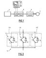
- a control chain of a rotary electrical machine 2 conventionally comprises a calculator 4 suitable for supplying power control instructions to an electronic igniter 6.
- the purpose of igniter 6 is to convert these power control instructions into control commands of a switch 10 of a switching device 8.
- the switching device 8 is for example a three-phase DC / AC converter. It includes six switches 10.
- This switch 10 comprises three packs 11A, 11B, 11C.
- Each pack 11A, 11B, 11C comprises an IGBT (Insulated Gate Bipolar Transistors) transistor 12, 14, 16 mounted antiparallel with its diode 18, 20, 22.
- Each power transistor comprises a gate electrode, a collector electrode and an emitter electrode hereinafter called gate, collector and emitter respectively.
- Each power transistor 12, 14, 16 is typically capable of switching currents up to 1200 A.
- the switch 10, i.e. the three transistors 12, 14, 16 connected in parallel, is capable of switching currents up to about 2500 A.
- Each power transistor 12, 14, 16 is capable of withstanding a voltage V CE between the collector and the transmitter in the off state, i.e. the open state, up to 4000 V, and in the on state, that is to say in the closed state, a voltage V CE generally less than 5 V.
- the igniter 6 is able to control the switching of the switch 10. It includes an encoder / decoder, a power system and a digital system not shown.
- the flash memory 23 is suitable for storing operating and control parameters of the power transistors 12, 14, 16. It is electrically erasable and rewritable. For this purpose, it is provided with electrical contacts adapted to be connected to a computer to modify the operating and control parameters of the power transistors 12, 14, 16, whenever the switching device 8 controls a new machine.
- the control device 24 is illustrated on the figure 3 . It is implanted in a user-programmable gate array, usually called FPGA component (Field Programmable Gate Array). It comprises control logic capable of controlling synchronously and independently three control circuits 26, 28, 30, each adapted to control a gate / emitter pair of a power transistor 12, 14, 16 of the switch 10. Only the control circuit 26 and the power transistor 12 have been illustrated on the figure 4 . The control circuits 28 and 30 are able to control the switching of the transistors 14 and 16 respectively. These circuits are identical to the circuit 26 and will not be described in detail.
- FPGA component Field Programmable Gate Array
- the power transistor 12 behaves as if it intrinsically included a capacitor, it was represented on the Figures 4 to 9 with a capacitor 32 connected to its gate and its transmitter.
- the circuit 26 is an H-bridge which serves to fix the potential between the gate and the emitter of the power transistor 12. It is delimited by a closed line and comprises two parallel electrical connections forming a first 33A and a second 33B vertical branches.
- the first branch 33A comprises a first MOS transistor 34, a first current generator 40 connected in parallel with a third MOS transistor 42.
- the first MOS transistor 34 is separated from the current generator assembly 40 - MOS transistor 42 by a midpoint 32A intended to be connected to the emitter of the power transistor 12.
- the second branch 33B comprises a second MOS transistor 36, a second current generator 44 connected in parallel with a fourth MOS transistor 46.
- the second transistor MOS 36 is separated from the current generator assembly 44 - fourth MOS transistor 46 by a second midpoint 32B intended to be connected to the gate.
- the generators 40 and 44 are variable resistance current generators digitally controlled via a not shown digital-to-analog converter.
- the control of the opening and closing of the MOS transistors 34, 36, 42, 46 is carried out directly by the control device 24 or by control units controlled by the control device 24.
- the MOS transistors 34, 42 and 36, 46 are switches whose function is to fix the polarity of the gate and the emitter of the power transistor 12 to circulate a current entering the gate of the power transistor 12 (current clockwise F1) or out of it (running counterclockwise F2).
- the H-bridge is powered by a capacitor 50 connected in a node 54 located between the MOS transistors 34 and 36, and in a node 56 located between the MOS transistor assemblies 34, 36 - current generators 40, 44.
- the voltage capacitor 50 is regulated at 15 V by a voltage source 57. This supplies the current required for operation by compensating for the inevitable joules losses in the gate control process of transistor 12.
- the control method of the circuit 26 begins with a step 58 in which it is verified that the capacitor 32 is not short-circuited due to, for example, a failure of a MOS transistor.
- the capacitor 32 If the capacitor 32 is not short-circuited, the voltage V GE between the gate and the emitter of the transistor 12 is initially charged to -15 V.
- step 60 the transistor 36 is closed, i.e. in an on state.
- Transistors 42 and 46 are in an open state, i.e., in a non-conducting state.
- Current generators 40, 44 are turned off or off, i.e. they do not generate current.
- a discharge current Ig of the capacitor 32 is established in the upper part of the clockwise H bridge F1 until the voltage between the gate and the emitter V GE of the transistor 12 is approximately equal to 0 V.
- the part of the circuit 26 in which the current Ig flows is illustrated on the figure 6 .
- the current Ig has a high intensity peak of between 5 and 10 A. This current peak makes it possible to bring the gate of the power transistor 12 to the conduction threshold.
- the voltage between the collector and the emitter V CE of transistor 12 is high (greater than the operating voltage divided by 2). No current flows between the collector and the emitter of the power transistor 12.
- the current generator 40 is energized to generate an Ig current.
- This current Ig is injected into the gate of the power transistor 12 via the capacitor 50 and the transistor 36, as visible on the figures 7 and 10 .
- the generator 40 is controlled so that the current Ig gradually decreases following a predefined curve profile P6, then the generator 40 is de-energized.
- the current profile P6 comprises a bearing at the moment when the power transistor 12 goes on, as illustrated on FIG. figure 10 , or varies according to an inverse exponential curve as illustrated on the figure 11 .
- the current generator 40 according to the invention is digitally controlled, the decrease of the current Ig is precisely regulated by the control device 24 in order to avoid any deterioration of the power transistor 12.
- this curve profile P6 can be easily modified when the switching device 8 is used for a new application, as explained later.
- a step 64 the transistor 42 is closed.
- the capacitor 50 discharges and generates a discharge pulse D visible on the figure 10 .
- This discharge pulse makes it possible to keep the power transistor 12 in the on state, avoiding successive opening and closing oscillatory phenomena which could damage the transistor 12.
- the voltage V CE is then approximately equal to 5 V.
- the voltage V GE between the gate and the emitter is +15 V.
- the voltage source 57 recharges the capacitor 50 to compensate for the Joule effect losses accumulated during the charging and discharging cycles of the capacitor 32.
- step 68 The opening procedure of the power transistors 12, 14, 16 starts with a step 68 during which the transistor 46 is closed (dashed lines on the figure 8 ), the transistors 34, 36 and 42 being open.
- a strong current Ig discharge capacitor 32 is established in the circuit 26 in the opposite direction of clockwise F2 as shown on the figures 8 and 10 . This reaches a value of 5 to 10 A depending on the type of IGBT.
- the voltage V GE is approximately equal to the conduction threshold voltage of the IGBT.
- the transistor 46 is open (shown in solid line on the figure 8 ) and the current generator 44 is energized. It generates a low intensity Ig current in the counterclockwise direction F2, as shown in FIG. figure 10 .
- the current Ig is gradually decreased by the current generator 44 and is optionally maintained at the same level when the power transistor 12 goes to the off state or not. Finally, the current generator 44 is de-energized.
- transistors 46 and 34 are closed.
- the capacitor 50 generates a discharge current pulse D illustrated on the figure 10 .
- the discharge of the capacitor 50 in the capacitor 32 makes it possible to quickly bring back the current flowing between the collector and the emitter of the power transistor 12 to a zero value.
- This pulse makes it possible to eliminate the oscillatory phenomenon that generally takes place during the opening of the new-generation power transistors. As the current Ic is quickly reduced to 0, the switching losses are reduced.
- the voltage source 57 recharges the capacitor 50 to compensate for the Joule effect losses accumulated during the charging and discharging cycles of the capacitor 32.
- the control device 24 comprises a control unit 79 able to decide which voltage V GE must be applied between the gate and the emitter of the transistors 12, 14, 16.
- the control unit 79 is a finite state machine, able to automatically switch from one control state to another when a condition of transition to the next state is satisfied.
- the control unit 79 is capable of converting the power control instructions of the computer 4 received by the encoder / decoder of the igniter 6 into control signals for injecting or extracting current in the gates of the power transistors 12, 14, 16.
- the control device 24 further comprises a memory 80, a peripheral logic unit 82 and an information acquisition circuit 84 relating to the voltage V CE between the collector and the emitter of the power transistors 12, 14, 16 .
- the memory 80 is a dual-port RAM RAM preloaded from the electrically programmable FLASH memory 23. It contains operating parameters of each power transistor 12, 14, 16, and current control parameters Ig intended to be applied to the gate and the emitter of each power transistor 12, 14, 16. These parameters are transferred from the flash memory 23 to the serial port of the memory 80 when the igniter 6 is turned on and are then able to be transferred from the 16-bit port of the memory 80 to program the peripheral logic unit 82 .
- the operating parameters and the control parameters can be easily modified by the connection of the flash memory 23 to a computer having a program for modifying these parameters.
- the acquisition circuit 84 is able to determine at any time the voltage V CE between the collector and the emitter of the power transistors 12, 14, 16, as well as the variation thereof with respect to time.
- the operating principle of this circuit is explained in the patent application published under number 02 851 056, and will not be described in this application.
- the control unit 79 is able to receive measurement information of the voltage V CE , as well as measurements of the variation of this voltage V CE with respect to time, of the acquisition circuit 84 to constantly monitor the coherence between the control commands received from the computer 4 with the state of each power transistor 12, 14, 16 both at the moment of switching and during the steady states.
- the peripheral logic unit 82 comprises a temporal filtering block 88 of the signals received from the acquisition circuit 84, a first 90 and a second 92 chronometers, a unit 94 for adjusting the profile of the current injected into the gate of the power transistors. 12, 14, 16 and finally a verification unit 96.
- the temporal filtering block 88 is capable of filtering the voltage V CE over a predefined time range in order to remove signals representative of parasitic variations therefrom.
- the first timer 90 is capable of timing times of the order of ten microseconds on command of the control unit 79. It is adapted to receive the memory 80 operating parameters and control parameters. These include in particular the minimum duration P1 of a pulse tolerated on the gate of each power transistor 12, 14, 16, as well as the minimum saturation delay P2 of each power transistor, that is to say the minimum delay between two switching commands. Examples of operating parameters and control parameters are illustrated on the figure 11 .
- the second timer 92 is able to measure times of 25 ⁇ s to a few microseconds on command of the control unit 79. It receives the parameters to time memory 80. It is used in particular to time moments P3, P4, P5 injection of the Ig currents in each gate of the power transistors 12, 14, 16 of the switch, the length of a current pulse P7, and the control time P8.
- the adjustment unit 94 is able to vary the supply current curves Ig1, Ig2, Ig3 of the power transistors 12, 14, 16 according to a P6 or several predefined current profiles received from the memory 80.
- current P6 can form a stair step like the one shown on the figure 10 or a decreasing exponential, as illustrated on the figure 11 .
- the control unit 94 is able to control the current generators 40 and 44 of the control circuits 26, 28 and 30. For this purpose, it is connected to analog digital converters, themselves connected to each of the generators 40, 44.
- the verification unit 96 receives commands from the control unit 79 to control driving units of the transistors 34, 36, 42 and 46.
- the verification unit 96 guarantees the non-conduction overlap of the MOS transistors.
- the verification unit 96 makes it possible to trigger the injection of the currents Ig1, Ig2, Ig3 into the gates of each of the transistors 12, 14, 16 at the predetermined moments P3, P4, P5.
- the operating parameters and the control parameters stored in the memory 80 comprise in particular the minimum duration P1 of a pulse tolerated on the gate of each power transistor, the minimum saturation delay P2, the moments P3, P4, P5 of current injection into each gate of the power transistors 12, 14, 16, and the profile P6 of the grid current decay.
- the control device 24 and the control circuits 26, 28, 30 make it possible to control all three transistors 12, 14, 16 accurately and quickly, taking into account the operating state of each of these power transistors. , the control device 24 being able to set up an emergency procedure in case of malfunction of one or more of these power transistors.
- the power transistors 12, 14, 16 have different moments of transition from the on state to the off state and vice versa. These differences in transition times from one state to another result from minor differences in the behavior of their silicon, and their position in the power switching loop.
- the industrial disparity of the parameters of the packs 11A, 11B, 11C and the slight dissymmetries of the switching loop thus provide imbalances in the instantaneous distribution of the current in the packs in parallel during the switching operations. This limits the use of the full breaking capacity of the packs in parallel assemblies.
- the first transistor of the switch that switches must withstand a higher transient current than the others until the other parallel-connected transistors are fully on. For this reason, it is necessary to limit the nominal commutation current of the converter, that is to say the current switched by the switch 10.
- the packs 11A, 11B, 11C are tested prior to their use in order to determine exactly the relative differences between them.
- the tripping moments P3, P4, P5 of the current Ig are determined as a function of these differences.
- the verification unit 96 of the control device triggers the powering up and the de-energizing of the current generators 40, 44 so that all the power transistors 12, 14, 16 go on at the same time. as illustrated on the figure 11 so that the nominal current of the converter can be increased.
- the current generators 40, 44 can be made by voltage regulators and amplifiers.
- the energy used to switch the power transistors 12, 14, 16 is dissipated in resistors while advantageously, in the present invention, this energy is recovered by the capacitor 50. Accordingly, the igniter 6 consumes less power and the components of the control circuits 26, 28, 30 are not heated and therefore not damaged.
- the driving principle of the gate / emitter pair of a power transistor used in the control circuit of the present invention makes it possible to dissipate energy on ignition of the power transistors only during reduced stages. This makes it possible to divide by a factor of 10 to 50 the energy dissipated by the circuits 26, 28, 30 during the ignition of the gates of the power transistors. Indeed, the energy is dissipated only during the steps 60 and 70 and it is not necessary to artificially increase the intrinsic capacitor 32 of the power transistors 12, 14, 16 by the addition of an additional external capacitor for adjust an RC circuit.
Landscapes
- Engineering & Computer Science (AREA)
- Power Engineering (AREA)
- Electronic Switches (AREA)
- Power Conversion In General (AREA)
- Ignition Installations For Internal Combustion Engines (AREA)
- Direct Current Feeding And Distribution (AREA)
- Control Of Direct Current Motors (AREA)
- Air Bags (AREA)
Priority Applications (1)
| Application Number | Priority Date | Filing Date | Title |
|---|---|---|---|
| PL09153034T PL2093868T3 (pl) | 2008-02-19 | 2009-02-17 | Urządzenie i obwód sterujący podzespołu elektronicznego mocy, powiązany sposób pilotowania i włącznik |
Applications Claiming Priority (1)
| Application Number | Priority Date | Filing Date | Title |
|---|---|---|---|
| FR0851046A FR2927738B1 (fr) | 2008-02-19 | 2008-02-19 | Dispositif et circuit de commande d'un composant electronique de puissance, procede de pilotage et allumeur associes. |
Publications (3)
| Publication Number | Publication Date |
|---|---|
| EP2093868A2 true EP2093868A2 (de) | 2009-08-26 |
| EP2093868A3 EP2093868A3 (de) | 2013-12-04 |
| EP2093868B1 EP2093868B1 (de) | 2017-04-12 |
Family
ID=39929952
Family Applications (1)
| Application Number | Title | Priority Date | Filing Date |
|---|---|---|---|
| EP09153034.5A Active EP2093868B1 (de) | 2008-02-19 | 2009-02-17 | Steuervorrichtung und -schaltkreis einer elektronischen Leistungskomponente, entsprechendes Steuerungsverfahren und entsprechende Zündvorrichtung |
Country Status (7)
| Country | Link |
|---|---|
| EP (1) | EP2093868B1 (de) |
| JP (1) | JP5322687B2 (de) |
| CN (1) | CN101521455B (de) |
| ES (1) | ES2628822T3 (de) |
| FR (1) | FR2927738B1 (de) |
| PL (1) | PL2093868T3 (de) |
| RU (1) | RU2485678C2 (de) |
Cited By (1)
| Publication number | Priority date | Publication date | Assignee | Title |
|---|---|---|---|---|
| CN102005990A (zh) * | 2010-11-12 | 2011-04-06 | 中国兵器工业集团第二一四研究所苏州研发中心 | 一种电机的h桥驱动控制电路 |
Families Citing this family (2)
| Publication number | Priority date | Publication date | Assignee | Title |
|---|---|---|---|---|
| RU170562U1 (ru) * | 2015-07-27 | 2017-04-28 | Акционерное общество "Калужский завод "Ремпутьмаш" | Система управления путевой машиной |
| JP7091819B2 (ja) | 2018-05-10 | 2022-06-28 | 富士電機株式会社 | ゲート駆動装置およびスイッチ装置 |
Family Cites Families (25)
| Publication number | Priority date | Publication date | Assignee | Title |
|---|---|---|---|---|
| US4859921A (en) * | 1988-03-10 | 1989-08-22 | General Electric Company | Electronic control circuits, electronically commutated motor systems, switching regulator power supplies, and methods |
| AU5508990A (en) * | 1989-05-18 | 1990-11-22 | Hirotami Nakano | Switching power supply apparatus and isolating method thereof |
| JP2760590B2 (ja) * | 1989-09-04 | 1998-06-04 | 株式会社東芝 | 電圧駆動形素子の駆動回路 |
| JPH06196978A (ja) * | 1992-12-25 | 1994-07-15 | Hitachi Denshi Ltd | 直流再生回路 |
| JP3052792B2 (ja) * | 1995-07-07 | 2000-06-19 | 株式会社デンソー | インバータ装置 |
| JPH10108477A (ja) * | 1996-09-30 | 1998-04-24 | Mitsutoyo Corp | インバータ回路 |
| JPH11205108A (ja) * | 1998-01-07 | 1999-07-30 | New Japan Radio Co Ltd | Npnトランジスタ駆動回路 |
| JPH11285239A (ja) * | 1998-03-27 | 1999-10-15 | Toyota Autom Loom Works Ltd | スイッチング素子を駆動する回路 |
| US6037720A (en) * | 1998-10-23 | 2000-03-14 | Philips Electronics North America Corporation | Level shifter |
| JP3941309B2 (ja) * | 1998-12-03 | 2007-07-04 | 株式会社日立製作所 | 電圧駆動形スイッチング素子のゲート駆動回路 |
| US6456511B1 (en) * | 2000-02-17 | 2002-09-24 | Tyco Electronics Corporation | Start-up circuit for flyback converter having secondary pulse width modulation |
| JP4145462B2 (ja) * | 2000-03-10 | 2008-09-03 | 株式会社リコー | スイッチング素子駆動回路装置およびそれを用いた電子機器 |
| JP2002094363A (ja) * | 2000-09-18 | 2002-03-29 | Toshiba Corp | 絶縁ゲート型半導体素子のゲート駆動回路、絶縁ゲート型半導体素子およびそれらを用いた電力変換装置 |
| JP4434510B2 (ja) * | 2001-03-16 | 2010-03-17 | 株式会社東芝 | 絶縁ゲート型半導体素子の故障検出方法および故障検出装置 |
| JP4382312B2 (ja) * | 2001-09-05 | 2009-12-09 | 三菱電機株式会社 | 駆動制御装置、電力変換装置、電力変換装置の制御方法、および電力変換装置の使用方法 |
| DE10211077A1 (de) * | 2002-03-13 | 2003-09-04 | Siemens Ag | Verfahren zur Ansteuerung von MOS-Gate gesteuerten Leistungshalbleitern |
| RU2223590C1 (ru) * | 2002-08-02 | 2004-02-10 | Ульяновский государственный технический университет | Мостовой инвертор |
| JP4044861B2 (ja) * | 2003-04-03 | 2008-02-06 | 三菱電機株式会社 | 電力変換装置およびその電力変換装置を備える電力変換システム装置 |
| RU31971U1 (ru) * | 2003-04-15 | 2003-09-10 | Белов Александр Михайлович | Устройство крышка-стерилизатор |
| TWI300650B (en) * | 2003-04-24 | 2008-09-01 | Int Rectifier Corp | Fault protected self-oscillating driver |
| TWI258261B (en) * | 2004-05-18 | 2006-07-11 | Richtek Techohnology Corp | JFET driving circuit applied to DC/DC converter and method thereof |
| DE102005016440A1 (de) * | 2005-04-01 | 2006-10-05 | Hantschel, Jochen, Dipl.-Ing. (FH) | Vorrichtung und Verfahren zur flexiblen Optimierung der Schaltvorgänge eines nichteinrastenden, abschaltbaren Leistungshalbleiters |
| JP4672575B2 (ja) * | 2006-03-08 | 2011-04-20 | 三菱電機株式会社 | パワーデバイスの駆動回路 |
| JP4442593B2 (ja) * | 2006-07-20 | 2010-03-31 | 株式会社日立製作所 | 電力変換装置 |
| RU59907U1 (ru) * | 2006-08-14 | 2006-12-27 | Дмитрий Владимирович Барыльник | Управляемое устройство для преобразования постоянного напряжения в переменное |
-
2008
- 2008-02-19 FR FR0851046A patent/FR2927738B1/fr not_active Expired - Fee Related
-
2009
- 2009-02-17 EP EP09153034.5A patent/EP2093868B1/de active Active
- 2009-02-17 PL PL09153034T patent/PL2093868T3/pl unknown
- 2009-02-17 ES ES09153034.5T patent/ES2628822T3/es active Active
- 2009-02-18 JP JP2009035225A patent/JP5322687B2/ja not_active Expired - Fee Related
- 2009-02-18 CN CN2009101346082A patent/CN101521455B/zh not_active Expired - Fee Related
- 2009-02-18 RU RU2009105731/07A patent/RU2485678C2/ru active
Cited By (2)
| Publication number | Priority date | Publication date | Assignee | Title |
|---|---|---|---|---|
| CN102005990A (zh) * | 2010-11-12 | 2011-04-06 | 中国兵器工业集团第二一四研究所苏州研发中心 | 一种电机的h桥驱动控制电路 |
| CN102005990B (zh) * | 2010-11-12 | 2013-09-18 | 中国兵器工业集团第二一四研究所苏州研发中心 | 一种电机的h桥驱动控制电路 |
Also Published As
| Publication number | Publication date |
|---|---|
| CN101521455A (zh) | 2009-09-02 |
| ES2628822T3 (es) | 2017-08-04 |
| JP5322687B2 (ja) | 2013-10-23 |
| PL2093868T3 (pl) | 2017-10-31 |
| CN101521455B (zh) | 2013-11-06 |
| RU2485678C2 (ru) | 2013-06-20 |
| EP2093868B1 (de) | 2017-04-12 |
| JP2009201110A (ja) | 2009-09-03 |
| EP2093868A3 (de) | 2013-12-04 |
| FR2927738B1 (fr) | 2013-01-04 |
| RU2009105731A (ru) | 2010-08-27 |
| FR2927738A1 (fr) | 2009-08-21 |
Similar Documents
| Publication | Publication Date | Title |
|---|---|---|
| EP3149853B1 (de) | Feldeffekttransistor und zugehörige fehlerdetektionsvorrichtung | |
| FR3075508A1 (fr) | Dispositif de commutation autoalimente et procede de fonctionnement d'un tel dispositif | |
| FR2659179A1 (fr) | Redresseur susceptible de fonctionner avec au moins deux plages distinctes de tension alternative d'alimentation. | |
| EP2008357B1 (de) | Schaltnetzwerk zur reihenimplementierung von igbt-transistoren | |
| EP2093868B1 (de) | Steuervorrichtung und -schaltkreis einer elektronischen Leistungskomponente, entsprechendes Steuerungsverfahren und entsprechende Zündvorrichtung | |
| EP3545621B1 (de) | Schaltelement für eine leistungsschaltung | |
| EP2346154B1 (de) | Einspeisungssystem eines Elements zwischen einem Rotor und einem Stator einer elektrischen Maschine, und Steuerungsverfahren eines solchen Systems | |
| EP3267583A1 (de) | Auswahlschaltkreis einer betriebsspannung mit kontolliertem übergang | |
| EP3087647B1 (de) | Leistungsregler mit linearer steuerung von stromspitzenbegrenzung und mit kurzschlussschutz | |
| FR2884079A1 (fr) | Commande d'un transistor mos | |
| EP2073367A1 (de) | Wechselspannungsgenerator ausgestattet mit einem Strombegrenzer | |
| EP1977514A1 (de) | Steuerung eines mos-transistors | |
| FR2923331A1 (fr) | Appareil electrique rotatif pour automobile | |
| EP3766169A1 (de) | Verfahren zur steuerung eines umrichters | |
| FR3004581A1 (fr) | Contacteur electrique et procede de pilotage d'une bobine electromagnetique dans un tel contacteur | |
| EP1070391B1 (de) | Verfahren und vorrichtung zum steuern eines leistungs-schalttransistors mit isoliertem gate | |
| FR2988933A1 (fr) | Generateur de courant et procede de generation d'impulsions de courant | |
| EP3185389B1 (de) | Vorrichtung und elektrisches gerät zur erzeugung einer elektrischen spannung für eine informationsbearbeitungseinheit, und entsprechendes elektronisches system zur informationsbearbeitung | |
| EP4576531A1 (de) | Elektronische vorrichtung und verfahren zur steuerung eines elektrischen energiewandlers mit synchronisiertem dreiecksignal und stromwandlersystem dafür | |
| WO2019229341A1 (fr) | Dispositif de commutation autoalimente et procede de fonctionnement d'un tel dispositif | |
| CA2462944A1 (fr) | Procede et systeme de commande d'urgence de la commutation d'un transistor de puissance | |
| FR3083390A1 (fr) | Procede de diagnostic d'un pont de puissance connecte a une machine electrique tournante | |
| FR3083394A1 (fr) | Dispositif de protection d'un composant de puissance pour un pont de transistors | |
| FR2795882A1 (fr) | Circuit de pilotage pour charge inductive | |
| FR3058844A1 (fr) | Circuit electrique pour un appareil electroportatif |
Legal Events
| Date | Code | Title | Description |
|---|---|---|---|
| PUAI | Public reference made under article 153(3) epc to a published international application that has entered the european phase |
Free format text: ORIGINAL CODE: 0009012 |
|
| AK | Designated contracting states |
Kind code of ref document: A2 Designated state(s): AT BE BG CH CY CZ DE DK EE ES FI FR GB GR HR HU IE IS IT LI LT LU LV MC MK MT NL NO PL PT RO SE SI SK TR |
|
| AX | Request for extension of the european patent |
Extension state: AL BA RS |
|
| PUAL | Search report despatched |
Free format text: ORIGINAL CODE: 0009013 |
|
| AK | Designated contracting states |
Kind code of ref document: A3 Designated state(s): AT BE BG CH CY CZ DE DK EE ES FI FR GB GR HR HU IE IS IT LI LT LU LV MC MK MT NL NO PL PT RO SE SI SK TR |
|
| AX | Request for extension of the european patent |
Extension state: AL BA RS |
|
| RIC1 | Information provided on ipc code assigned before grant |
Ipc: H02M 1/08 20060101AFI20131025BHEP Ipc: H03K 17/16 20060101ALI20131025BHEP Ipc: H03K 17/567 20060101ALI20131025BHEP Ipc: H03K 17/66 20060101ALI20131025BHEP |
|
| 17P | Request for examination filed |
Effective date: 20140604 |
|
| RBV | Designated contracting states (corrected) |
Designated state(s): AT BE BG CH CY CZ DE DK EE ES FI FR GB GR HR HU IE IS IT LI LT LU LV MC MK MT NL NO PL PT RO SE SI SK TR |
|
| AKX | Designation fees paid |
Designated state(s): AT BE BG CH CY CZ DE DK EE ES FI FR GB GR HR HU IE IS IT LI LT LU LV MC MK MT NL NO PL PT RO SE SI SK TR |
|
| RAP1 | Party data changed (applicant data changed or rights of an application transferred) |
Owner name: ALSTOM TRANSPORT TECHNOLOGIES |
|
| RAP1 | Party data changed (applicant data changed or rights of an application transferred) |
Owner name: ALSTOM TRANSPORT TECHNOLOGIES |
|
| GRAP | Despatch of communication of intention to grant a patent |
Free format text: ORIGINAL CODE: EPIDOSNIGR1 |
|
| RIC1 | Information provided on ipc code assigned before grant |
Ipc: H03K 17/16 20060101ALI20161012BHEP Ipc: H03K 17/66 20060101ALI20161012BHEP Ipc: H02M 1/08 20060101AFI20161012BHEP Ipc: H03K 17/12 20060101ALI20161012BHEP Ipc: H03K 17/567 20060101ALI20161012BHEP |
|
| INTG | Intention to grant announced |
Effective date: 20161102 |
|
| GRAS | Grant fee paid |
Free format text: ORIGINAL CODE: EPIDOSNIGR3 |
|
| GRAA | (expected) grant |
Free format text: ORIGINAL CODE: 0009210 |
|
| AK | Designated contracting states |
Kind code of ref document: B1 Designated state(s): AT BE BG CH CY CZ DE DK EE ES FI FR GB GR HR HU IE IS IT LI LT LU LV MC MK MT NL NO PL PT RO SE SI SK TR |
|
| REG | Reference to a national code |
Ref country code: GB Ref legal event code: FG4D Free format text: NOT ENGLISH |
|
| REG | Reference to a national code |
Ref country code: CH Ref legal event code: EP |
|
| REG | Reference to a national code |
Ref country code: IE Ref legal event code: FG4D Free format text: LANGUAGE OF EP DOCUMENT: FRENCH |
|
| REG | Reference to a national code |
Ref country code: AT Ref legal event code: REF Ref document number: 884776 Country of ref document: AT Kind code of ref document: T Effective date: 20170515 |
|
| REG | Reference to a national code |
Ref country code: DE Ref legal event code: R096 Ref document number: 602009045332 Country of ref document: DE |
|
| REG | Reference to a national code |
Ref country code: NL Ref legal event code: FP |
|
| REG | Reference to a national code |
Ref country code: SE Ref legal event code: TRGR |
|
| REG | Reference to a national code |
Ref country code: ES Ref legal event code: FG2A Ref document number: 2628822 Country of ref document: ES Kind code of ref document: T3 Effective date: 20170804 |
|
| REG | Reference to a national code |
Ref country code: LT Ref legal event code: MG4D |
|
| REG | Reference to a national code |
Ref country code: AT Ref legal event code: MK05 Ref document number: 884776 Country of ref document: AT Kind code of ref document: T Effective date: 20170412 |
|
| PG25 | Lapsed in a contracting state [announced via postgrant information from national office to epo] |
Ref country code: LT Free format text: LAPSE BECAUSE OF FAILURE TO SUBMIT A TRANSLATION OF THE DESCRIPTION OR TO PAY THE FEE WITHIN THE PRESCRIBED TIME-LIMIT Effective date: 20170412 Ref country code: FI Free format text: LAPSE BECAUSE OF FAILURE TO SUBMIT A TRANSLATION OF THE DESCRIPTION OR TO PAY THE FEE WITHIN THE PRESCRIBED TIME-LIMIT Effective date: 20170412 Ref country code: HR Free format text: LAPSE BECAUSE OF FAILURE TO SUBMIT A TRANSLATION OF THE DESCRIPTION OR TO PAY THE FEE WITHIN THE PRESCRIBED TIME-LIMIT Effective date: 20170412 Ref country code: AT Free format text: LAPSE BECAUSE OF FAILURE TO SUBMIT A TRANSLATION OF THE DESCRIPTION OR TO PAY THE FEE WITHIN THE PRESCRIBED TIME-LIMIT Effective date: 20170412 Ref country code: GR Free format text: LAPSE BECAUSE OF FAILURE TO SUBMIT A TRANSLATION OF THE DESCRIPTION OR TO PAY THE FEE WITHIN THE PRESCRIBED TIME-LIMIT Effective date: 20170713 Ref country code: NO Free format text: LAPSE BECAUSE OF FAILURE TO SUBMIT A TRANSLATION OF THE DESCRIPTION OR TO PAY THE FEE WITHIN THE PRESCRIBED TIME-LIMIT Effective date: 20170712 |
|
| PG25 | Lapsed in a contracting state [announced via postgrant information from national office to epo] |
Ref country code: LV Free format text: LAPSE BECAUSE OF FAILURE TO SUBMIT A TRANSLATION OF THE DESCRIPTION OR TO PAY THE FEE WITHIN THE PRESCRIBED TIME-LIMIT Effective date: 20170412 Ref country code: BG Free format text: LAPSE BECAUSE OF FAILURE TO SUBMIT A TRANSLATION OF THE DESCRIPTION OR TO PAY THE FEE WITHIN THE PRESCRIBED TIME-LIMIT Effective date: 20170712 Ref country code: IS Free format text: LAPSE BECAUSE OF FAILURE TO SUBMIT A TRANSLATION OF THE DESCRIPTION OR TO PAY THE FEE WITHIN THE PRESCRIBED TIME-LIMIT Effective date: 20170812 |
|
| REG | Reference to a national code |
Ref country code: DE Ref legal event code: R097 Ref document number: 602009045332 Country of ref document: DE |
|
| PG25 | Lapsed in a contracting state [announced via postgrant information from national office to epo] |
Ref country code: SK Free format text: LAPSE BECAUSE OF FAILURE TO SUBMIT A TRANSLATION OF THE DESCRIPTION OR TO PAY THE FEE WITHIN THE PRESCRIBED TIME-LIMIT Effective date: 20170412 Ref country code: DK Free format text: LAPSE BECAUSE OF FAILURE TO SUBMIT A TRANSLATION OF THE DESCRIPTION OR TO PAY THE FEE WITHIN THE PRESCRIBED TIME-LIMIT Effective date: 20170412 Ref country code: EE Free format text: LAPSE BECAUSE OF FAILURE TO SUBMIT A TRANSLATION OF THE DESCRIPTION OR TO PAY THE FEE WITHIN THE PRESCRIBED TIME-LIMIT Effective date: 20170412 Ref country code: CZ Free format text: LAPSE BECAUSE OF FAILURE TO SUBMIT A TRANSLATION OF THE DESCRIPTION OR TO PAY THE FEE WITHIN THE PRESCRIBED TIME-LIMIT Effective date: 20170412 Ref country code: RO Free format text: LAPSE BECAUSE OF FAILURE TO SUBMIT A TRANSLATION OF THE DESCRIPTION OR TO PAY THE FEE WITHIN THE PRESCRIBED TIME-LIMIT Effective date: 20170412 |
|
| PLBE | No opposition filed within time limit |
Free format text: ORIGINAL CODE: 0009261 |
|
| STAA | Information on the status of an ep patent application or granted ep patent |
Free format text: STATUS: NO OPPOSITION FILED WITHIN TIME LIMIT |
|
| REG | Reference to a national code |
Ref country code: FR Ref legal event code: PLFP Year of fee payment: 10 |
|
| 26N | No opposition filed |
Effective date: 20180115 |
|
| PG25 | Lapsed in a contracting state [announced via postgrant information from national office to epo] |
Ref country code: SI Free format text: LAPSE BECAUSE OF FAILURE TO SUBMIT A TRANSLATION OF THE DESCRIPTION OR TO PAY THE FEE WITHIN THE PRESCRIBED TIME-LIMIT Effective date: 20170412 |
|
| REG | Reference to a national code |
Ref country code: CH Ref legal event code: PL |
|
| PG25 | Lapsed in a contracting state [announced via postgrant information from national office to epo] |
Ref country code: MT Free format text: LAPSE BECAUSE OF FAILURE TO SUBMIT A TRANSLATION OF THE DESCRIPTION OR TO PAY THE FEE WITHIN THE PRESCRIBED TIME-LIMIT Effective date: 20170412 Ref country code: MC Free format text: LAPSE BECAUSE OF FAILURE TO SUBMIT A TRANSLATION OF THE DESCRIPTION OR TO PAY THE FEE WITHIN THE PRESCRIBED TIME-LIMIT Effective date: 20170412 |
|
| REG | Reference to a national code |
Ref country code: IE Ref legal event code: MM4A |
|
| PG25 | Lapsed in a contracting state [announced via postgrant information from national office to epo] |
Ref country code: LU Free format text: LAPSE BECAUSE OF NON-PAYMENT OF DUE FEES Effective date: 20180217 Ref country code: CH Free format text: LAPSE BECAUSE OF NON-PAYMENT OF DUE FEES Effective date: 20180228 Ref country code: LI Free format text: LAPSE BECAUSE OF NON-PAYMENT OF DUE FEES Effective date: 20180228 |
|
| PG25 | Lapsed in a contracting state [announced via postgrant information from national office to epo] |
Ref country code: IE Free format text: LAPSE BECAUSE OF NON-PAYMENT OF DUE FEES Effective date: 20180217 |
|
| PG25 | Lapsed in a contracting state [announced via postgrant information from national office to epo] |
Ref country code: TR Free format text: LAPSE BECAUSE OF FAILURE TO SUBMIT A TRANSLATION OF THE DESCRIPTION OR TO PAY THE FEE WITHIN THE PRESCRIBED TIME-LIMIT Effective date: 20170412 |
|
| PG25 | Lapsed in a contracting state [announced via postgrant information from national office to epo] |
Ref country code: HU Free format text: LAPSE BECAUSE OF FAILURE TO SUBMIT A TRANSLATION OF THE DESCRIPTION OR TO PAY THE FEE WITHIN THE PRESCRIBED TIME-LIMIT; INVALID AB INITIO Effective date: 20090217 Ref country code: PT Free format text: LAPSE BECAUSE OF FAILURE TO SUBMIT A TRANSLATION OF THE DESCRIPTION OR TO PAY THE FEE WITHIN THE PRESCRIBED TIME-LIMIT Effective date: 20170412 |
|
| PG25 | Lapsed in a contracting state [announced via postgrant information from national office to epo] |
Ref country code: MK Free format text: LAPSE BECAUSE OF NON-PAYMENT OF DUE FEES Effective date: 20170412 Ref country code: CY Free format text: LAPSE BECAUSE OF FAILURE TO SUBMIT A TRANSLATION OF THE DESCRIPTION OR TO PAY THE FEE WITHIN THE PRESCRIBED TIME-LIMIT Effective date: 20170412 |
|
| PGFP | Annual fee paid to national office [announced via postgrant information from national office to epo] |
Ref country code: GB Payment date: 20220223 Year of fee payment: 14 |
|
| PGFP | Annual fee paid to national office [announced via postgrant information from national office to epo] |
Ref country code: SE Payment date: 20220216 Year of fee payment: 14 Ref country code: PL Payment date: 20220203 Year of fee payment: 14 |
|
| REG | Reference to a national code |
Ref country code: SE Ref legal event code: EUG |
|
| GBPC | Gb: european patent ceased through non-payment of renewal fee |
Effective date: 20230217 |
|
| PG25 | Lapsed in a contracting state [announced via postgrant information from national office to epo] |
Ref country code: SE Free format text: LAPSE BECAUSE OF NON-PAYMENT OF DUE FEES Effective date: 20230218 |
|
| P01 | Opt-out of the competence of the unified patent court (upc) registered |
Effective date: 20231025 |
|
| PG25 | Lapsed in a contracting state [announced via postgrant information from national office to epo] |
Ref country code: GB Free format text: LAPSE BECAUSE OF NON-PAYMENT OF DUE FEES Effective date: 20230217 |
|
| PG25 | Lapsed in a contracting state [announced via postgrant information from national office to epo] |
Ref country code: GB Free format text: LAPSE BECAUSE OF NON-PAYMENT OF DUE FEES Effective date: 20230217 |
|
| PG25 | Lapsed in a contracting state [announced via postgrant information from national office to epo] |
Ref country code: PL Free format text: LAPSE BECAUSE OF NON-PAYMENT OF DUE FEES Effective date: 20230217 |
|
| PG25 | Lapsed in a contracting state [announced via postgrant information from national office to epo] |
Ref country code: PL Free format text: LAPSE BECAUSE OF NON-PAYMENT OF DUE FEES Effective date: 20230217 |
|
| REG | Reference to a national code |
Ref country code: ES Ref legal event code: PC2A Owner name: ALSTOM HOLDINGS Effective date: 20250310 |
|
| PGFP | Annual fee paid to national office [announced via postgrant information from national office to epo] |
Ref country code: NL Payment date: 20250218 Year of fee payment: 17 |
|
| PGFP | Annual fee paid to national office [announced via postgrant information from national office to epo] |
Ref country code: DE Payment date: 20250218 Year of fee payment: 17 |
|
| PGFP | Annual fee paid to national office [announced via postgrant information from national office to epo] |
Ref country code: ES Payment date: 20250328 Year of fee payment: 17 |
|
| PGFP | Annual fee paid to national office [announced via postgrant information from national office to epo] |
Ref country code: BE Payment date: 20250218 Year of fee payment: 17 |
|
| PGFP | Annual fee paid to national office [announced via postgrant information from national office to epo] |
Ref country code: FR Payment date: 20250221 Year of fee payment: 17 |
|
| PGFP | Annual fee paid to national office [announced via postgrant information from national office to epo] |
Ref country code: IT Payment date: 20250224 Year of fee payment: 17 |
|
| REG | Reference to a national code |
Ref country code: BE Ref legal event code: PD Owner name: ALSTOM HOLDINGS; FR Free format text: DETAILS ASSIGNMENT: CHANGE OF OWNER(S), ASSIGNMENT; FORMER OWNER NAME: ALSTOM TRANSPORT TECHNOLOGIES Effective date: 20241025 |