EP2093873A2 - Gleichrichter - Google Patents
Gleichrichter Download PDFInfo
- Publication number
- EP2093873A2 EP2093873A2 EP08103420A EP08103420A EP2093873A2 EP 2093873 A2 EP2093873 A2 EP 2093873A2 EP 08103420 A EP08103420 A EP 08103420A EP 08103420 A EP08103420 A EP 08103420A EP 2093873 A2 EP2093873 A2 EP 2093873A2
- Authority
- EP
- European Patent Office
- Prior art keywords
- switch
- voltage
- rectifier
- pad
- secondary side
- Prior art date
- Legal status (The legal status is an assumption and is not a legal conclusion. Google has not performed a legal analysis and makes no representation as to the accuracy of the status listed.)
- Granted
Links
- 230000001105 regulatory effect Effects 0.000 claims abstract description 30
- 239000003990 capacitor Substances 0.000 claims abstract description 7
- 239000004065 semiconductor Substances 0.000 claims description 6
- 238000000034 method Methods 0.000 claims description 4
- 230000005669 field effect Effects 0.000 claims description 2
- 229910044991 metal oxide Inorganic materials 0.000 claims description 2
- 150000004706 metal oxides Chemical class 0.000 claims description 2
- 230000010354 integration Effects 0.000 abstract description 4
- 238000006243 chemical reaction Methods 0.000 description 2
- 230000002459 sustained effect Effects 0.000 description 2
- 230000000694 effects Effects 0.000 description 1
Images


Classifications
-
- H—ELECTRICITY
- H02—GENERATION; CONVERSION OR DISTRIBUTION OF ELECTRIC POWER
- H02M—APPARATUS FOR CONVERSION BETWEEN AC AND AC, BETWEEN AC AND DC, OR BETWEEN DC AND DC, AND FOR USE WITH MAINS OR SIMILAR POWER SUPPLY SYSTEMS; CONVERSION OF DC OR AC INPUT POWER INTO SURGE OUTPUT POWER; CONTROL OR REGULATION THEREOF
- H02M3/00—Conversion of DC power input into DC power output
- H02M3/02—Conversion of DC power input into DC power output without intermediate conversion into AC
- H02M3/04—Conversion of DC power input into DC power output without intermediate conversion into AC by static converters
- H02M3/10—Conversion of DC power input into DC power output without intermediate conversion into AC by static converters using discharge tubes with control electrode or semiconductor devices with control electrode
- H02M3/145—Conversion of DC power input into DC power output without intermediate conversion into AC by static converters using discharge tubes with control electrode or semiconductor devices with control electrode using devices of a triode or transistor type requiring continuous application of a control signal
- H02M3/155—Conversion of DC power input into DC power output without intermediate conversion into AC by static converters using discharge tubes with control electrode or semiconductor devices with control electrode using devices of a triode or transistor type requiring continuous application of a control signal using semiconductor devices only
-
- H—ELECTRICITY
- H02—GENERATION; CONVERSION OR DISTRIBUTION OF ELECTRIC POWER
- H02M—APPARATUS FOR CONVERSION BETWEEN AC AND AC, BETWEEN AC AND DC, OR BETWEEN DC AND DC, AND FOR USE WITH MAINS OR SIMILAR POWER SUPPLY SYSTEMS; CONVERSION OF DC OR AC INPUT POWER INTO SURGE OUTPUT POWER; CONTROL OR REGULATION THEREOF
- H02M1/00—Details of apparatus for conversion
- H02M1/42—Circuits or arrangements for compensating for or adjusting power factor in converters or inverters
- H02M1/4208—Arrangements for improving power factor of AC input
- H02M1/4225—Arrangements for improving power factor of AC input using a non-isolated boost converter
-
- H—ELECTRICITY
- H02—GENERATION; CONVERSION OR DISTRIBUTION OF ELECTRIC POWER
- H02M—APPARATUS FOR CONVERSION BETWEEN AC AND AC, BETWEEN AC AND DC, OR BETWEEN DC AND DC, AND FOR USE WITH MAINS OR SIMILAR POWER SUPPLY SYSTEMS; CONVERSION OF DC OR AC INPUT POWER INTO SURGE OUTPUT POWER; CONTROL OR REGULATION THEREOF
- H02M7/00—Conversion of AC power input into DC power output; Conversion of DC power input into AC power output
- H02M7/02—Conversion of AC power input into DC power output without possibility of reversal
- H02M7/04—Conversion of AC power input into DC power output without possibility of reversal by static converters
- H02M7/12—Conversion of AC power input into DC power output without possibility of reversal by static converters using discharge tubes with control electrode or semiconductor devices with control electrode
- H02M7/145—Conversion of AC power input into DC power output without possibility of reversal by static converters using discharge tubes with control electrode or semiconductor devices with control electrode using devices of a thyratron or thyristor type requiring extinguishing means
- H02M7/155—Conversion of AC power input into DC power output without possibility of reversal by static converters using discharge tubes with control electrode or semiconductor devices with control electrode using devices of a thyratron or thyristor type requiring extinguishing means using semiconductor devices only
-
- H—ELECTRICITY
- H02—GENERATION; CONVERSION OR DISTRIBUTION OF ELECTRIC POWER
- H02M—APPARATUS FOR CONVERSION BETWEEN AC AND AC, BETWEEN AC AND DC, OR BETWEEN DC AND DC, AND FOR USE WITH MAINS OR SIMILAR POWER SUPPLY SYSTEMS; CONVERSION OF DC OR AC INPUT POWER INTO SURGE OUTPUT POWER; CONTROL OR REGULATION THEREOF
- H02M7/00—Conversion of AC power input into DC power output; Conversion of DC power input into AC power output
- H02M7/02—Conversion of AC power input into DC power output without possibility of reversal
- H02M7/04—Conversion of AC power input into DC power output without possibility of reversal by static converters
- H02M7/12—Conversion of AC power input into DC power output without possibility of reversal by static converters using discharge tubes with control electrode or semiconductor devices with control electrode
- H02M7/21—Conversion of AC power input into DC power output without possibility of reversal by static converters using discharge tubes with control electrode or semiconductor devices with control electrode using devices of a triode or transistor type requiring continuous application of a control signal
- H02M7/217—Conversion of AC power input into DC power output without possibility of reversal by static converters using discharge tubes with control electrode or semiconductor devices with control electrode using devices of a triode or transistor type requiring continuous application of a control signal using semiconductor devices only
- H02M7/2176—Conversion of AC power input into DC power output without possibility of reversal by static converters using discharge tubes with control electrode or semiconductor devices with control electrode using devices of a triode or transistor type requiring continuous application of a control signal using semiconductor devices only comprising a passive stage to generate a rectified sinusoidal voltage and a controlled switching element in series between such stage and the output
-
- Y—GENERAL TAGGING OF NEW TECHNOLOGICAL DEVELOPMENTS; GENERAL TAGGING OF CROSS-SECTIONAL TECHNOLOGIES SPANNING OVER SEVERAL SECTIONS OF THE IPC; TECHNICAL SUBJECTS COVERED BY FORMER USPC CROSS-REFERENCE ART COLLECTIONS [XRACs] AND DIGESTS
- Y02—TECHNOLOGIES OR APPLICATIONS FOR MITIGATION OR ADAPTATION AGAINST CLIMATE CHANGE
- Y02B—CLIMATE CHANGE MITIGATION TECHNOLOGIES RELATED TO BUILDINGS, e.g. HOUSING, HOUSE APPLIANCES OR RELATED END-USER APPLICATIONS
- Y02B70/00—Technologies for an efficient end-user side electric power management and consumption
- Y02B70/10—Technologies improving the efficiency by using switched-mode power supplies [SMPS], i.e. efficient power electronics conversion e.g. power factor correction or reduction of losses in power supplies or efficient standby modes
Definitions
- the present invention relates to a powering circuit of an AC-DC converter, and in particular, to a powering circuit of an AC-DC converter that turns on a switch only when an AC input voltage is lower than a preset reference voltage and sustaining a DC output voltage in a stable DC bias range.
- a conventional AC-DC converter adopts an isolated voltage divider design.
- an external transformer converts a high AC power supply into a low-voltage DC power supply for a low-voltage DC power supply device.
- the external transformer has a large volume, which goes against the demands for miniaturization.
- linear regulators such as low dropout voltage regulator (LDO) are provided to solve the above problem, but the power consumption of switches of the LDO may easily cause unsatisfactory conversion efficiency.
- An AC-DC converter circuit without the use of a transformer capable of outputting a stable constant current US Patent Publication No. 2002/0044471 , has been put forward by the applicant of the present invention.
- This AC-DC converter circuit is applicable to a load device such as a light-emitting element (for example, an LED) in need of a stable current supply.
- a current switching circuit is used to limit a load current within a stable range.
- a control circuit is used to determine the on/off state of the current switching circuit according to the potential difference between the output and input of the control circuit. When the potential difference is lower than a preset value, the control circuit switches on the load current, and when the potential difference is higher than a preset value, the control circuit switches off the load current, thereby achieving the effect of limiting the load current.
- US Patent No. 6,169,391 B1 has also disclosed an AC-DC converter circuit without the use of a transformer.
- a control circuit functioning similarly to a linear regulator is employed to limit the output voltage of a DC power supply.
- the control circuit has a sensing circuit for detecting an input voltage Vin of an AC power supply, and controls the on/off state of a switch according to the value of the input voltage Vin.
- the sensing circuit is comprised of two voltage divider resistors connected in series and a zener diode connected in series to the voltage divider resistor.
- such circuit design is obviously complex.
- the present invention is directed to a powering circuit of an AC-DC converter capable of reducing the power consumption of a switch.
- the powering circuit includes a rectifier, a sensing circuit, a control switching circuit, and a voltage regulating capacitor.
- the rectifier has a primary side coupled to an AC power supply, for converting the AC power supply into a DC power supply.
- the sensing circuit is connected to a secondary side of the rectifier, for detecting an AC input voltage of the AC power supply. When the AC input voltage is lower than a preset reference voltage (Vref), a second switch in the control switching circuit is turned on, thereby providing a low DC output voltage.
- Vref preset reference voltage
- the control switching circuit sustains the DC output voltage in a stable DC bias range.
- the second switch is turned on only when the AC input voltage is lower than the preset reference voltage, and is turned off when the AC input voltage is higher than a preset voltage.
- the potential difference between the input and output in the course of the on state of the second switch is small, the power consumption of the second switch can be reduced.
- the present invention is also directed to a powering circuit of an AC-DC converter with a simple circuit structure.
- the powering circuit includes a rectifier, a sensing circuit, a control switching circuit, and a voltage regulating capacitor.
- the sensing circuit has a voltage divider and a first switch.
- the sensing circuit uses the voltage divider to obtain a divided DC voltage of a DC power supply at a secondary side of the rectifier, and compares the divided DC voltage with a turn-on voltage of the first switch, for turning off the first switch when the divided DC voltage is lower than the turn-on voltage.
- the second switch is turned on when the DC voltage of the DC power supply at the secondary side of the rectifier is lower than the preset reference voltage, and is turned off when the DC voltage of the DC power supply at the secondary side of the rectifier is higher than the preset reference voltage.
- the present invention is further directed to a powering circuit of an AC-DC converter capable of realizing integration.
- the first and second switches may be fabricated in a semiconductor process, thus achieving the purpose of circuit integration.
- the circuit architecture is used to convert a high AC input voltage AC Vin of an AC power supply 10 into a low DC output voltage DC Vout. Then, the DC output voltage DC Vout stabilized in a DC bias range is output through a low-voltage DC output end 42, so as to provide a load voltage stabilized in a DC bias range for a low-voltage DC power supply device 11 (for example, an integrated circuit or a miniaturized electronic product).
- the circuit architecture includes a rectifier 20, a sensing circuit 30, a control switching circuit 40, and a voltage regulating capacitor 60.
- the rectifier 20 has a primary side coupled to the AC power supply 10 and a secondary side for outputting a DC power supply DC.
- the rectifier 20 may be a full-wave bridge rectifier or a half-wave bridge rectifier.
- the sensing circuit 30 has a voltage divider 31 and a first switch Q1.
- the voltage divider 31 is coupled to the secondary side of the rectifier 20 so as to obtain a divided DC voltage of the DC power supply at the secondary side.
- the first switch Q1 has a control pad 1a, an input pad 1b, and an output pad 1c.
- the output pad 1c is connected to ground potential, and the control pad 1a is connected to the voltage divider 31.
- the sensing circuit 30 compares the divided DC voltage with a turn-on voltage of the first switch Q1, for turning off the first switch Q1 when the divided DC voltage is lower than the turn-on voltage.
- the control switching circuit 40 has a third resistor R3, a second switch Q2, and a first voltage regulating element 41 (for example, but not limited to, a zener diode).
- the second switch Q2 has a control pad 2a, an input pad 2b, and an output pad 2c.
- the input pad 2b of the second switch Q2 is connected to the secondary side of the rectifier 20, and the control pad 2a is connected to the input pad 1b of the first switch Q1.
- the second switch Q2 is turned on to send the DC power supply at the secondary side of the rectifier 20 to the DC output end 42 of the control switching circuit 40 through the output pad 2c, thereby outputting a DC output voltage DC Vout.
- the voltage level of the DC output voltage DC Vout is clamped by the first voltage regulating element 41, and is lower than a clamping voltage level of the first voltage regulating element 41.
- the voltage regulating capacitor 60 is connected at one end to the DC output end 42 of the control switching circuit 40 and at the other end to ground potential, so as to provide a DC output voltage DC Vout stabilized in a DC bias range and serving as a load voltage required by the low-voltage DC power supply device 11.
- the present invention further provides several specific embodiments of the circuit as follows.
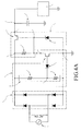
- FIGs. 2A and 2B show a first specific embodiment of the circuit.
- the rectifier 20 is a full-wave bridge rectifier in FIG. 2A , and a half-wave bridge rectifier in FIG. 2B .
- the first switch Q1 and the second switch Q2 are power metal oxide semiconductor field effect transistors (MOSFET), and preferably, N-MOSFETs. Since N-MOSFETs can be fabricated in a semiconductor process, the powering circuit of an AC-DC converter of the present invention can also be fabricated in the semiconductor process, thereby achieving the purpose of integration.
- the voltage divider 31 includes a first resistor R1 and a second resistor R2 connected in series to the first resistor R1.
- the first resistor R1 is connected at one end to the secondary side of the rectifier 20, and at the other end to the second resistor R2 and a gate G of the first switch Q1.
- the second resistor R2 is connected at one end to the first resistor R1 and the gate of the first switch Q1, and the other end of the second resistor R2 and a source S of the first switch Q1 are both connected to ground potential.
- the sensing circuit 30 determines the on/off state of the second switch Q2 according to the value of the AC input voltage AC Vin.
- the withstand voltage of the first switch Q1 must be higher than the divided DC voltage of the first resistor R1 and the second resistor R2.
- the control switching circuit 40 has a third resistor R3.
- the third resistor R3 is connected at one end to the secondary side of the rectifier 20, and at the other end to a drain D of the first switch Q1 and a cathode of the first voltage regulating element 41, so as to prevent the first voltage regulating element 41 of the control switching circuit 40 from being damaged by an over-high current.
- the first voltage regulating element 41 has an anode connected to ground potential.
- the second switch Q2 has a gate G connected to the drain of the first switch Q1 and the cathode of the first voltage regulating element 41, a drain D connected to the secondary side of the rectifier 20, and a source S connected to the DC output end 42.
- the gate-source of the first switch Q1 when the divided DC voltage is higher than the turn-on voltage of the first switch Q1, the gate-source of the first switch Q1 generates a forward bias to make the first switch Q1 assume an on state, i.e., turn on the first switch Q1.
- the first voltage regulating element 41 is at a low level, and the second switch Q2 cannot be turned on, and the DC power supply DC at the secondary side of the rectifier 20 will not be provided to the DC output end 42.
- the first switch Q1 when the divided DC voltage is lower than the turn-on voltage of the first switch Q1, the first switch Q1 is turned off, and the voltage level of the first voltage regulating element 41 with a voltage clamp function will rise increasingly.
- the second switch Q2 when the DC voltage of the DC power supply at the secondary side of the rectifier 20 is lower than the preset reference voltage Vref, the second switch Q2 is turned on, and the DC output end 42 outputs a low DC output voltage DC Vout.
- the voltage level of the DC output voltage DC Vout may also be clamped by the first voltage regulating element 41 to be lower than the clamping voltage level of the first voltage regulating element 41.
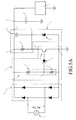
- FIGs. 3A and 3B respectively show another embodiment of FIGs. 2A and 2B .
- the embodiment of FIG. 3A further includes a second voltage regulating element 44 (for example, but not limited to, a zener diode).
- the second voltage regulating element 44 has a cathode connected to the gate G of the first switch Q1, and an anode connected to ground potential. Through the voltage clamp function of the second voltage regulating element 44, the voltage level between the gate and the source of the first switch Q1 is clamped, so as to prevent the first switch Q1 from being damaged by an over-high AC input voltage.
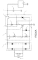
- FIGs. 4A and 4B respectively show another embodiment of FIGs. 3A and 3B .
- the first switch Q1 and the second switch Q2 are both bi-polar junction transistors (BJTs), and the second voltage regulating element 44 is connected in series between the voltage divider 31 and a base of the first switch Q1 (BJT), so as to protect the first switch Q1 from being damaged by an over-high AC input voltage.
- BJTs bi-polar junction transistors
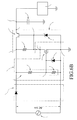
- the second switch Q2 in FIGs. 4A and 4B is an N-MOSFET having a circuit as shown in FIGs. 5A and 5B respectively.
- the second switch Q2 in FIGs. 3A and 3B is a BJT having a circuit as shown in FIGs. 6A and 6B respectively.
- the powering circuit of an AC-DC converter of the present invention is directly adapted to a common commercial power voltage (for example, 110-10 VAC or 220-240 VAC at a frequency of 50-60 Hz), for converting a high AC input voltage AC Vin into a low DC output voltage DC Vout.
- the reference voltage Vref of a reference power supply serves as a preset voltage for determining the on state (turn on)/off state (turn off) of the second switch Q2.
- the reference voltage Vref the turn-on voltage of the first switch Q1 ⁇ (R1+R2)/R2.
- the voltage-current relationship between the AC input voltage AC Vin and the DC output end 42 is indicated by the curve of FIG. 7 (in which the circuit using a full-wave bridge rectifier 20 in FIG.
- the voltage V is a drain-source voltage Vds of the second switch Q2, and the reference voltage Vref is, for example, 70 DC V.
- Vds drain-source voltage
- Vref reference voltage
- the divided DC voltage is higher than the turn-on voltage of the first switch Q1
- the first switch Q1 is turned on
- the second switch Q2 is turned off.
- a drain current I D of the second switch Q2 is 0.
- the divided DC voltage is lower than the turn-on voltage of the first switch Q 1
- the first switch Q1 is turned off.
- the voltage drop at two ends of the first voltage regulating element 41 increasingly rises to a clamping voltage of the first voltage regulating element 41.
- the second switch Q2 is turned on, and the DC output end 42 outputs a low DC output voltage DC Vout.
- the voltage level of the DC output voltage DC Vout may also be clamped by the first voltage regulating element 41 to be lower than the clamping voltage level of the first voltage regulating element 41.
- the DC output voltage DC Vout of the DC output end 42 is sustained in a stable DC bias range.
- the powering circuit of an AC-DC converter of the present invention turns on the second switch Q2 only when the AC input voltage AC Vin is lower than the preset reference voltage Vref, and turns off the second switch Q2 when the AC input voltage AC Vin is higher than the preset reference voltage Vref.
- the advantage of the present invention resides in that when the second switch Q2 is in the on state (turned on), the potential difference between the input and output is low, thus reducing the power consumption of the switch.
- the second switch Q2 is in the on state (turned on)
- the voltage level of the DC output voltage DC Vout is clamped by the first voltage regulating element 41 to be lower than the clamping voltage level of the first voltage regulating element 41.
- the DC output voltage DC Vout is sustained in a stable DC bias range.
Landscapes
- Engineering & Computer Science (AREA)
- Power Engineering (AREA)
- Rectifiers (AREA)
- Dc-Dc Converters (AREA)
Applications Claiming Priority (1)
| Application Number | Priority Date | Filing Date | Title |
|---|---|---|---|
| TW097106374A TW200937828A (en) | 2008-02-22 | 2008-02-22 | Electricity -extraction circuit of AC/DC converter take |
Publications (3)
| Publication Number | Publication Date |
|---|---|
| EP2093873A2 true EP2093873A2 (de) | 2009-08-26 |
| EP2093873A3 EP2093873A3 (de) | 2012-08-29 |
| EP2093873B1 EP2093873B1 (de) | 2018-11-21 |
Family
ID=39500407
Family Applications (1)
| Application Number | Title | Priority Date | Filing Date |
|---|---|---|---|
| EP08103420.9A Not-in-force EP2093873B1 (de) | 2008-02-22 | 2008-04-08 | Gleichrichter |
Country Status (5)
| Country | Link |
|---|---|
| US (1) | US7715216B2 (de) |
| EP (1) | EP2093873B1 (de) |
| JP (1) | JP2009201342A (de) |
| KR (1) | KR100988266B1 (de) |
| TW (1) | TW200937828A (de) |
Families Citing this family (50)
| Publication number | Priority date | Publication date | Assignee | Title |
|---|---|---|---|---|
| JP2009164415A (ja) * | 2008-01-08 | 2009-07-23 | Mitsumi Electric Co Ltd | 半導体装置 |
| CN201378801Y (zh) * | 2009-02-17 | 2010-01-06 | 中山大洋电机股份有限公司 | 一种ac/dc变换电路及其应用的电机控制器 |
| EP2496056B1 (de) * | 2009-10-26 | 2014-08-20 | Airtec System Co., Ltd. | Mit konstantstrom betriebene led-modulvorrichtung |
| CN102201664A (zh) * | 2010-03-25 | 2011-09-28 | 鸿富锦精密工业(深圳)有限公司 | 稳压电路系统 |
| US8816654B2 (en) | 2010-09-27 | 2014-08-26 | Cooper Technologies Company | Universal-voltage discrete input circuit |
| JP2012152066A (ja) * | 2011-01-20 | 2012-08-09 | Olympus Corp | 電源装置 |
| US9256239B2 (en) * | 2011-03-17 | 2016-02-09 | Watlow Electric Manufacturing Company | Voltage controlling circuit |
| CN102185500A (zh) * | 2011-04-28 | 2011-09-14 | 刘家发 | 实用的无变压器开关电源 |
| CA2738844C (en) * | 2011-05-04 | 2012-04-24 | Itron, Inc. | Full wave ac/dc voltage divider |
| TWI514743B (zh) * | 2011-08-24 | 2015-12-21 | Tsung Ein Tsai | 可調功因之隔離式無變壓器交流轉直流電源電路 |
| US9252652B2 (en) * | 2011-11-16 | 2016-02-02 | Rockwell Automation Technologies, Inc. | Wide input voltage range power supply circuit |
| US8890494B2 (en) | 2011-11-16 | 2014-11-18 | Rockwell Automation Technologies, Inc. | Wide input voltage range power supply circuit |
| KR101887108B1 (ko) * | 2011-11-21 | 2018-08-10 | 에이치피프린팅코리아 주식회사 | 과전압 차단 기능을 구비한 스위칭 모드 전원 공급장치와 이를 이용한 과전압 차단 방법 및 화상 형성 장치 |
| CN102594175B (zh) * | 2012-03-06 | 2014-06-25 | 广州金升阳科技有限公司 | 一种交流变直流电路 |
| US8917076B2 (en) * | 2012-08-10 | 2014-12-23 | Monolithic Power Systems, Inc. | Off-line regulator with pass device and associated method |
| US8890427B2 (en) * | 2012-10-26 | 2014-11-18 | Liteideas, Llc | Apparatus and method of operation of a low-current LED lighting circuit |
| TWI464569B (zh) * | 2012-11-06 | 2014-12-11 | Upi Semiconductor Corp | 電壓識別碼參考電壓產生電路與其開機電壓產生方法 |
| US9155232B2 (en) | 2013-01-10 | 2015-10-06 | Rockwell Automation Technologies, Inc. | Wide input voltage range power supply circuit |
| WO2014146070A1 (en) * | 2013-03-15 | 2014-09-18 | Tagnetics, Inc. | Apparatus and system of power conversion |
| WO2014179189A1 (en) | 2013-04-30 | 2014-11-06 | Tagnetics, Inc. | Lighted mounting apparatus |
| US9219416B2 (en) | 2013-11-30 | 2015-12-22 | Ixys Corporation | Buck converter having self-driven BJT synchronous rectifier |
| US20160013789A1 (en) * | 2014-07-09 | 2016-01-14 | Numerex Corp. | Depletion Mode MOSFET Power Supply |
| WO2017196571A1 (en) * | 2016-05-07 | 2017-11-16 | Mark Telefus | High efficiency ac to dc converter and methods |
| JP7076430B2 (ja) * | 2016-05-07 | 2022-05-27 | インテレソル,エルエルシー | ソリッドステート配線不良回路遮断器 |
| US10931473B2 (en) | 2016-10-20 | 2021-02-23 | Intelesol, Llc | Building automation system |
| KR102399201B1 (ko) | 2016-10-28 | 2022-05-17 | 인테레솔, 엘엘씨 | 부하를 식별하는 ac 전력 공급원의 제어 및 방법 |
| WO2018080604A1 (en) * | 2016-10-28 | 2018-05-03 | Mark Telefus | High efficiency ac direct to dc extraction converter and methods |
| WO2019117205A1 (ja) * | 2017-12-12 | 2019-06-20 | パーソルAvcテクノロジー株式会社 | 発光ダイオード駆動装置 |
| TWI695560B (zh) | 2018-06-15 | 2020-06-01 | 群光電能科技股份有限公司 | 電源供應系統及電源轉換器 |
| US11671029B2 (en) | 2018-07-07 | 2023-06-06 | Intelesol, Llc | AC to DC converters |
| US11581725B2 (en) | 2018-07-07 | 2023-02-14 | Intelesol, Llc | Solid-state power interrupters |
| US11056981B2 (en) * | 2018-07-07 | 2021-07-06 | Intelesol, Llc | Method and apparatus for signal extraction with sample and hold and release |
| US11205011B2 (en) | 2018-09-27 | 2021-12-21 | Amber Solutions, Inc. | Privacy and the management of permissions |
| US11334388B2 (en) | 2018-09-27 | 2022-05-17 | Amber Solutions, Inc. | Infrastructure support to enhance resource-constrained device capabilities |
| US11349296B2 (en) | 2018-10-01 | 2022-05-31 | Intelesol, Llc | Solid-state circuit interrupters |
| US10985548B2 (en) | 2018-10-01 | 2021-04-20 | Intelesol, Llc | Circuit interrupter with optical connection |
| JP7475351B2 (ja) | 2018-12-17 | 2024-04-26 | インテレソール エルエルシー | Ac駆動型の発光ダイオードシステム |
| US11422520B2 (en) | 2019-04-08 | 2022-08-23 | Intelesol, Llc | Building automation system |
| US11336199B2 (en) | 2019-04-09 | 2022-05-17 | Intelesol, Llc | Load identifying AC power supply with control and methods |
| US11373831B2 (en) | 2019-05-18 | 2022-06-28 | Amber Solutions, Inc. | Intelligent circuit breakers |
| EP4088125A4 (de) | 2020-01-21 | 2024-03-06 | Amber Semiconductor, Inc. | Intelligente schaltungsunterbrechung |
| US12231056B2 (en) | 2020-03-09 | 2025-02-18 | Intelesol, Llc | Integrated energy supply system and methods to provide regulated AC and low voltage DC |
| US12095383B2 (en) | 2020-03-09 | 2024-09-17 | Intelesol, Llc | AC to DC converter |
| TWI713287B (zh) * | 2020-03-19 | 2020-12-11 | 捷拓科技股份有限公司 | 寬輸入電壓範圍的輔助電源供應電路 |
| CN113691247A (zh) * | 2020-05-18 | 2021-11-23 | 湖南工业大学 | 一种远程交直流开关信号匹配器 |
| CN116195158B (zh) | 2020-08-11 | 2024-09-10 | 安泊半导体公司 | 智能能源监测和选择控制系统 |
| US12113525B2 (en) | 2021-09-30 | 2024-10-08 | Amber Semiconductor, Inc. | Intelligent electrical switches |
| US12348028B2 (en) | 2021-10-22 | 2025-07-01 | Amber Semiconductor, Inc. | Multi-output programmable power manager |
| US12362646B2 (en) | 2022-01-26 | 2025-07-15 | Amber Semiconductor, Inc. | Controlling AC power to inductive loads |
| CN115498746B (zh) * | 2022-11-07 | 2023-03-28 | 广东希荻微电子股份有限公司 | 供电电路与供电方法、电子设备 |
Citations (2)
| Publication number | Priority date | Publication date | Assignee | Title |
|---|---|---|---|---|
| US6169391B1 (en) | 1999-07-12 | 2001-01-02 | Supertex, Inc. | Device for converting high voltage alternating current to low voltage direct current |
| US20020044471A1 (en) | 2001-08-20 | 2002-04-18 | Te-Cheng Chen | Transformerless AC/DC converting control circuit |
Family Cites Families (12)
| Publication number | Priority date | Publication date | Assignee | Title |
|---|---|---|---|---|
| US3818273A (en) * | 1971-03-26 | 1974-06-18 | Yokogawa Electric Works Ltd | Barrier isolator device employing an overload protection circuit |
| US3777253A (en) * | 1972-10-24 | 1973-12-04 | Allen Bradley Co | Low power loss voltage supply circuit |
| US4001668A (en) * | 1973-11-16 | 1977-01-04 | Schick Incorporated | Electric shaver operable from a wide range of supply voltages |
| GB2124804A (en) * | 1982-07-16 | 1984-02-22 | Philips Electronic Associated | Electrical power supply arrangements |
| DE3245238A1 (de) * | 1982-12-07 | 1984-06-07 | Siemens AG, 1000 Berlin und 8000 München | Transformatorlose schaltungsanordnung zur erzeugung kleiner gleichspannungen |
| US4685046A (en) * | 1985-10-03 | 1987-08-04 | The Scott & Fetzer Company | Low voltage direct current power supply |
| JPH0638522A (ja) * | 1992-07-17 | 1994-02-10 | Nippon Telegr & Teleph Corp <Ntt> | スイッチング電源装置 |
| JPH07222439A (ja) * | 1994-02-02 | 1995-08-18 | Fuji Electric Co Ltd | Dc−dcコンバータ |
| KR19990049087A (ko) * | 1997-12-11 | 1999-07-05 | 김영환 | 전원공급기의 출력커패시터 방전 장치 |
| EP1166420B1 (de) * | 1999-03-31 | 2003-05-07 | Pepperl + Fuchs Gmbh | Sicherheitsbarriere zum begrenzen von strom und spannung |
| US6366437B1 (en) * | 1999-06-24 | 2002-04-02 | Relcom, Inc. | Current limiter for a network |
| JP3784594B2 (ja) * | 1999-11-30 | 2006-06-14 | 富士通株式会社 | 電流制御回路 |
-
2008
- 2008-02-22 TW TW097106374A patent/TW200937828A/zh unknown
- 2008-04-07 US US12/098,512 patent/US7715216B2/en active Active
- 2008-04-08 EP EP08103420.9A patent/EP2093873B1/de not_active Not-in-force
- 2008-04-18 JP JP2008108760A patent/JP2009201342A/ja active Pending
- 2008-04-18 KR KR1020080036110A patent/KR100988266B1/ko not_active Expired - Fee Related
Patent Citations (2)
| Publication number | Priority date | Publication date | Assignee | Title |
|---|---|---|---|---|
| US6169391B1 (en) | 1999-07-12 | 2001-01-02 | Supertex, Inc. | Device for converting high voltage alternating current to low voltage direct current |
| US20020044471A1 (en) | 2001-08-20 | 2002-04-18 | Te-Cheng Chen | Transformerless AC/DC converting control circuit |
Also Published As
| Publication number | Publication date |
|---|---|
| JP2009201342A (ja) | 2009-09-03 |
| EP2093873B1 (de) | 2018-11-21 |
| TW200937828A (en) | 2009-09-01 |
| KR20090090972A (ko) | 2009-08-26 |
| US7715216B2 (en) | 2010-05-11 |
| EP2093873A3 (de) | 2012-08-29 |
| KR100988266B1 (ko) | 2010-10-18 |
| US20090213629A1 (en) | 2009-08-27 |
| TWI343697B (de) | 2011-06-11 |
Similar Documents
| Publication | Publication Date | Title |
|---|---|---|
| EP2093873B1 (de) | Gleichrichter | |
| US9391525B2 (en) | Power system switch protection using output driver regulation | |
| US8358517B2 (en) | Switching power conversion circuit and power supply using same | |
| EP3076537A1 (de) | Stromquellenvorrichtung und elektrische vorrichtung | |
| US8987999B2 (en) | LED driver | |
| US20130021013A1 (en) | Switching power supply apparatus | |
| US20050225360A1 (en) | Voltage detection circuit, power supply unit and semiconductor device | |
| KR101489962B1 (ko) | 전력 변환기, 그 스위칭 제어 장치 및 구동 방법 | |
| CN110134026B (zh) | 一种用于智能家电的低功耗控制电路 | |
| KR101319284B1 (ko) | Dc-dc 컨버터 및 전원 장치 | |
| KR100593926B1 (ko) | 동기 정류기를 갖는 플라이백 컨버터 | |
| KR100568319B1 (ko) | 동기 정류기를 갖는 플라이백 컨버터 | |
| US9509210B2 (en) | Start-up circuit and method for AC-DC converters | |
| TWI499348B (zh) | 具有電荷突波保護之負載驅動電路 | |
| US11297702B2 (en) | Dimmer interface circuit and buffer stage circuit thereof | |
| JP2000245150A (ja) | スイッチング電源回路およびスイッチング電源用デバイス | |
| CN101534064B (zh) | 交直流转换器的取电电路 | |
| EP3112973A1 (de) | Konstantspannungversorgungsschaltung für einen schutzschalter | |
| US8400072B2 (en) | Light emitting device driver circuit driving light emitting device by positive and negative voltages and method for driving light emitting device by positive and negative voltages | |
| CN210199529U (zh) | 一种用于智能家电的低功耗控制电路和智能家电系统 | |
| EP2804303B1 (de) | Schaltnetzteil | |
| TW202542676A (zh) | 隨電流動態調整電壓餘裕的電源轉換器 | |
| US7542309B2 (en) | Voltage stabilizer circuit of forward converter | |
| US9077256B2 (en) | Method of forming a low power dissipation regulator and structure therefor | |
| KR101284827B1 (ko) | 스위치 제어 장치, 스위치 제어 방법 및 이를 이용하는컨버터 |
Legal Events
| Date | Code | Title | Description |
|---|---|---|---|
| PUAI | Public reference made under article 153(3) epc to a published international application that has entered the european phase |
Free format text: ORIGINAL CODE: 0009012 |
|
| 17P | Request for examination filed |
Effective date: 20080408 |
|
| AK | Designated contracting states |
Kind code of ref document: A2 Designated state(s): AT BE BG CH CY CZ DE DK EE ES FI FR GB GR HR HU IE IS IT LI LT LU LV MC MT NL NO PL PT RO SE SI SK TR |
|
| AX | Request for extension of the european patent |
Extension state: AL BA MK RS |
|
| PUAL | Search report despatched |
Free format text: ORIGINAL CODE: 0009013 |
|
| AK | Designated contracting states |
Kind code of ref document: A3 Designated state(s): AT BE BG CH CY CZ DE DK EE ES FI FR GB GR HR HU IE IS IT LI LT LU LV MC MT NL NO PL PT RO SE SI SK TR |
|
| AX | Request for extension of the european patent |
Extension state: AL BA MK RS |
|
| RIC1 | Information provided on ipc code assigned before grant |
Ipc: H02M 3/155 20060101AFI20120724BHEP Ipc: H02M 7/217 20060101ALI20120724BHEP |
|
| AKX | Designation fees paid |
Designated state(s): AT BE BG CH CY CZ DE DK EE ES FI FR GB GR HR HU IE IS IT LI LT LU LV MC MT NL NO PL PT RO SE SI SK TR |
|
| 17Q | First examination report despatched |
Effective date: 20160425 |
|
| STAA | Information on the status of an ep patent application or granted ep patent |
Free format text: STATUS: EXAMINATION IS IN PROGRESS |
|
| GRAP | Despatch of communication of intention to grant a patent |
Free format text: ORIGINAL CODE: EPIDOSNIGR1 |
|
| STAA | Information on the status of an ep patent application or granted ep patent |
Free format text: STATUS: GRANT OF PATENT IS INTENDED |
|
| INTG | Intention to grant announced |
Effective date: 20180720 |
|
| GRAS | Grant fee paid |
Free format text: ORIGINAL CODE: EPIDOSNIGR3 |
|
| GRAA | (expected) grant |
Free format text: ORIGINAL CODE: 0009210 |
|
| STAA | Information on the status of an ep patent application or granted ep patent |
Free format text: STATUS: THE PATENT HAS BEEN GRANTED |
|
| AK | Designated contracting states |
Kind code of ref document: B1 Designated state(s): AT BE BG CH CY CZ DE DK EE ES FI FR GB GR HR HU IE IS IT LI LT LU LV MC MT NL NO PL PT RO SE SI SK TR |
|
| RAP1 | Party data changed (applicant data changed or rights of an application transferred) |
Owner name: MACROBLOCK INC. |
|
| REG | Reference to a national code |
Ref country code: CH Ref legal event code: EP |
|
| REG | Reference to a national code |
Ref country code: IE Ref legal event code: FG4D |
|
| REG | Reference to a national code |
Ref country code: DE Ref legal event code: R096 Ref document number: 602008057985 Country of ref document: DE |
|
| REG | Reference to a national code |
Ref country code: AT Ref legal event code: REF Ref document number: 1068706 Country of ref document: AT Kind code of ref document: T Effective date: 20181215 |
|
| REG | Reference to a national code |
Ref country code: NL Ref legal event code: MP Effective date: 20181121 |
|
| REG | Reference to a national code |
Ref country code: AT Ref legal event code: MK05 Ref document number: 1068706 Country of ref document: AT Kind code of ref document: T Effective date: 20181121 |
|
| PG25 | Lapsed in a contracting state [announced via postgrant information from national office to epo] |
Ref country code: FI Free format text: LAPSE BECAUSE OF FAILURE TO SUBMIT A TRANSLATION OF THE DESCRIPTION OR TO PAY THE FEE WITHIN THE PRESCRIBED TIME-LIMIT Effective date: 20181121 Ref country code: BG Free format text: LAPSE BECAUSE OF FAILURE TO SUBMIT A TRANSLATION OF THE DESCRIPTION OR TO PAY THE FEE WITHIN THE PRESCRIBED TIME-LIMIT Effective date: 20190221 Ref country code: HR Free format text: LAPSE BECAUSE OF FAILURE TO SUBMIT A TRANSLATION OF THE DESCRIPTION OR TO PAY THE FEE WITHIN THE PRESCRIBED TIME-LIMIT Effective date: 20181121 Ref country code: LV Free format text: LAPSE BECAUSE OF FAILURE TO SUBMIT A TRANSLATION OF THE DESCRIPTION OR TO PAY THE FEE WITHIN THE PRESCRIBED TIME-LIMIT Effective date: 20181121 Ref country code: ES Free format text: LAPSE BECAUSE OF FAILURE TO SUBMIT A TRANSLATION OF THE DESCRIPTION OR TO PAY THE FEE WITHIN THE PRESCRIBED TIME-LIMIT Effective date: 20181121 Ref country code: AT Free format text: LAPSE BECAUSE OF FAILURE TO SUBMIT A TRANSLATION OF THE DESCRIPTION OR TO PAY THE FEE WITHIN THE PRESCRIBED TIME-LIMIT Effective date: 20181121 Ref country code: NO Free format text: LAPSE BECAUSE OF FAILURE TO SUBMIT A TRANSLATION OF THE DESCRIPTION OR TO PAY THE FEE WITHIN THE PRESCRIBED TIME-LIMIT Effective date: 20190221 Ref country code: LT Free format text: LAPSE BECAUSE OF FAILURE TO SUBMIT A TRANSLATION OF THE DESCRIPTION OR TO PAY THE FEE WITHIN THE PRESCRIBED TIME-LIMIT Effective date: 20181121 Ref country code: IS Free format text: LAPSE BECAUSE OF FAILURE TO SUBMIT A TRANSLATION OF THE DESCRIPTION OR TO PAY THE FEE WITHIN THE PRESCRIBED TIME-LIMIT Effective date: 20190321 |
|
| PG25 | Lapsed in a contracting state [announced via postgrant information from national office to epo] |
Ref country code: NL Free format text: LAPSE BECAUSE OF FAILURE TO SUBMIT A TRANSLATION OF THE DESCRIPTION OR TO PAY THE FEE WITHIN THE PRESCRIBED TIME-LIMIT Effective date: 20181121 Ref country code: PT Free format text: LAPSE BECAUSE OF FAILURE TO SUBMIT A TRANSLATION OF THE DESCRIPTION OR TO PAY THE FEE WITHIN THE PRESCRIBED TIME-LIMIT Effective date: 20190321 Ref country code: GR Free format text: LAPSE BECAUSE OF FAILURE TO SUBMIT A TRANSLATION OF THE DESCRIPTION OR TO PAY THE FEE WITHIN THE PRESCRIBED TIME-LIMIT Effective date: 20190222 Ref country code: SE Free format text: LAPSE BECAUSE OF FAILURE TO SUBMIT A TRANSLATION OF THE DESCRIPTION OR TO PAY THE FEE WITHIN THE PRESCRIBED TIME-LIMIT Effective date: 20181121 |
|
| PG25 | Lapsed in a contracting state [announced via postgrant information from national office to epo] |
Ref country code: IT Free format text: LAPSE BECAUSE OF FAILURE TO SUBMIT A TRANSLATION OF THE DESCRIPTION OR TO PAY THE FEE WITHIN THE PRESCRIBED TIME-LIMIT Effective date: 20181121 Ref country code: CZ Free format text: LAPSE BECAUSE OF FAILURE TO SUBMIT A TRANSLATION OF THE DESCRIPTION OR TO PAY THE FEE WITHIN THE PRESCRIBED TIME-LIMIT Effective date: 20181121 Ref country code: DK Free format text: LAPSE BECAUSE OF FAILURE TO SUBMIT A TRANSLATION OF THE DESCRIPTION OR TO PAY THE FEE WITHIN THE PRESCRIBED TIME-LIMIT Effective date: 20181121 Ref country code: PL Free format text: LAPSE BECAUSE OF FAILURE TO SUBMIT A TRANSLATION OF THE DESCRIPTION OR TO PAY THE FEE WITHIN THE PRESCRIBED TIME-LIMIT Effective date: 20181121 |
|
| REG | Reference to a national code |
Ref country code: DE Ref legal event code: R097 Ref document number: 602008057985 Country of ref document: DE |
|
| PG25 | Lapsed in a contracting state [announced via postgrant information from national office to epo] |
Ref country code: EE Free format text: LAPSE BECAUSE OF FAILURE TO SUBMIT A TRANSLATION OF THE DESCRIPTION OR TO PAY THE FEE WITHIN THE PRESCRIBED TIME-LIMIT Effective date: 20181121 Ref country code: SK Free format text: LAPSE BECAUSE OF FAILURE TO SUBMIT A TRANSLATION OF THE DESCRIPTION OR TO PAY THE FEE WITHIN THE PRESCRIBED TIME-LIMIT Effective date: 20181121 Ref country code: RO Free format text: LAPSE BECAUSE OF FAILURE TO SUBMIT A TRANSLATION OF THE DESCRIPTION OR TO PAY THE FEE WITHIN THE PRESCRIBED TIME-LIMIT Effective date: 20181121 |
|
| PLBE | No opposition filed within time limit |
Free format text: ORIGINAL CODE: 0009261 |
|
| STAA | Information on the status of an ep patent application or granted ep patent |
Free format text: STATUS: NO OPPOSITION FILED WITHIN TIME LIMIT |
|
| 26N | No opposition filed |
Effective date: 20190822 |
|
| PG25 | Lapsed in a contracting state [announced via postgrant information from national office to epo] |
Ref country code: SI Free format text: LAPSE BECAUSE OF FAILURE TO SUBMIT A TRANSLATION OF THE DESCRIPTION OR TO PAY THE FEE WITHIN THE PRESCRIBED TIME-LIMIT Effective date: 20181121 |
|
| REG | Reference to a national code |
Ref country code: DE Ref legal event code: R119 Ref document number: 602008057985 Country of ref document: DE |
|
| REG | Reference to a national code |
Ref country code: CH Ref legal event code: PL |
|
| REG | Reference to a national code |
Ref country code: BE Ref legal event code: MM Effective date: 20190430 |
|
| GBPC | Gb: european patent ceased through non-payment of renewal fee |
Effective date: 20190408 |
|
| PG25 | Lapsed in a contracting state [announced via postgrant information from national office to epo] |
Ref country code: MC Free format text: LAPSE BECAUSE OF FAILURE TO SUBMIT A TRANSLATION OF THE DESCRIPTION OR TO PAY THE FEE WITHIN THE PRESCRIBED TIME-LIMIT Effective date: 20181121 Ref country code: LU Free format text: LAPSE BECAUSE OF NON-PAYMENT OF DUE FEES Effective date: 20190408 |
|
| PG25 | Lapsed in a contracting state [announced via postgrant information from national office to epo] |
Ref country code: LI Free format text: LAPSE BECAUSE OF NON-PAYMENT OF DUE FEES Effective date: 20190430 Ref country code: CH Free format text: LAPSE BECAUSE OF NON-PAYMENT OF DUE FEES Effective date: 20190430 Ref country code: GB Free format text: LAPSE BECAUSE OF NON-PAYMENT OF DUE FEES Effective date: 20190408 Ref country code: DE Free format text: LAPSE BECAUSE OF NON-PAYMENT OF DUE FEES Effective date: 20191101 |
|
| PG25 | Lapsed in a contracting state [announced via postgrant information from national office to epo] |
Ref country code: FR Free format text: LAPSE BECAUSE OF NON-PAYMENT OF DUE FEES Effective date: 20190430 Ref country code: BE Free format text: LAPSE BECAUSE OF NON-PAYMENT OF DUE FEES Effective date: 20190430 |
|
| PG25 | Lapsed in a contracting state [announced via postgrant information from national office to epo] |
Ref country code: TR Free format text: LAPSE BECAUSE OF FAILURE TO SUBMIT A TRANSLATION OF THE DESCRIPTION OR TO PAY THE FEE WITHIN THE PRESCRIBED TIME-LIMIT Effective date: 20181121 |
|
| PG25 | Lapsed in a contracting state [announced via postgrant information from national office to epo] |
Ref country code: IE Free format text: LAPSE BECAUSE OF NON-PAYMENT OF DUE FEES Effective date: 20190408 |
|
| PG25 | Lapsed in a contracting state [announced via postgrant information from national office to epo] |
Ref country code: CY Free format text: LAPSE BECAUSE OF FAILURE TO SUBMIT A TRANSLATION OF THE DESCRIPTION OR TO PAY THE FEE WITHIN THE PRESCRIBED TIME-LIMIT Effective date: 20181121 |
|
| PG25 | Lapsed in a contracting state [announced via postgrant information from national office to epo] |
Ref country code: HU Free format text: LAPSE BECAUSE OF FAILURE TO SUBMIT A TRANSLATION OF THE DESCRIPTION OR TO PAY THE FEE WITHIN THE PRESCRIBED TIME-LIMIT; INVALID AB INITIO Effective date: 20080408 Ref country code: MT Free format text: LAPSE BECAUSE OF FAILURE TO SUBMIT A TRANSLATION OF THE DESCRIPTION OR TO PAY THE FEE WITHIN THE PRESCRIBED TIME-LIMIT Effective date: 20181121 |