EP2096659B1 - Elektronenemissionsquelle, elektrische Vorrichtung damit und Herstellungsverfahren dafür - Google Patents
Elektronenemissionsquelle, elektrische Vorrichtung damit und Herstellungsverfahren dafür Download PDFInfo
- Publication number
- EP2096659B1 EP2096659B1 EP08157123A EP08157123A EP2096659B1 EP 2096659 B1 EP2096659 B1 EP 2096659B1 EP 08157123 A EP08157123 A EP 08157123A EP 08157123 A EP08157123 A EP 08157123A EP 2096659 B1 EP2096659 B1 EP 2096659B1
- Authority
- EP
- European Patent Office
- Prior art keywords
- electron emission
- cathode
- cnt
- emission source
- layer
- Prior art date
- Legal status (The legal status is an assumption and is not a legal conclusion. Google has not performed a legal analysis and makes no representation as to the accuracy of the status listed.)
- Ceased
Links
- 238000004519 manufacturing process Methods 0.000 title claims description 32
- 239000010410 layer Substances 0.000 claims description 99
- 238000000034 method Methods 0.000 claims description 71
- 239000000725 suspension Substances 0.000 claims description 64
- 239000000758 substrate Substances 0.000 claims description 46
- 239000012790 adhesive layer Substances 0.000 claims description 43
- 239000000463 material Substances 0.000 claims description 36
- 230000008569 process Effects 0.000 claims description 34
- 239000000853 adhesive Substances 0.000 claims description 9
- 230000001070 adhesive effect Effects 0.000 claims description 9
- 239000002390 adhesive tape Substances 0.000 claims description 6
- OAICVXFJPJFONN-UHFFFAOYSA-N Phosphorus Chemical compound [P] OAICVXFJPJFONN-UHFFFAOYSA-N 0.000 claims description 5
- 238000001035 drying Methods 0.000 claims description 5
- 238000003825 pressing Methods 0.000 claims 1
- OKTJSMMVPCPJKN-UHFFFAOYSA-N Carbon Chemical compound [C] OKTJSMMVPCPJKN-UHFFFAOYSA-N 0.000 description 261
- 239000002041 carbon nanotube Substances 0.000 description 258
- 229910021393 carbon nanotube Inorganic materials 0.000 description 256
- 230000005684 electric field Effects 0.000 description 46
- 239000010409 thin film Substances 0.000 description 27
- 239000000843 powder Substances 0.000 description 12
- 238000001914 filtration Methods 0.000 description 9
- 238000003466 welding Methods 0.000 description 9
- 239000004020 conductor Substances 0.000 description 8
- 238000012360 testing method Methods 0.000 description 7
- PXHVJJICTQNCMI-UHFFFAOYSA-N Nickel Chemical compound [Ni] PXHVJJICTQNCMI-UHFFFAOYSA-N 0.000 description 6
- 229910052751 metal Inorganic materials 0.000 description 6
- 239000002184 metal Substances 0.000 description 6
- 239000004094 surface-active agent Substances 0.000 description 6
- 239000011230 binding agent Substances 0.000 description 5
- 229910052799 carbon Inorganic materials 0.000 description 5
- 238000000151 deposition Methods 0.000 description 5
- 238000001962 electrophoresis Methods 0.000 description 5
- 239000002245 particle Substances 0.000 description 5
- 238000007639 printing Methods 0.000 description 5
- 239000002904 solvent Substances 0.000 description 5
- 230000003197 catalytic effect Effects 0.000 description 4
- 229920000642 polymer Polymers 0.000 description 4
- 239000011734 sodium Substances 0.000 description 4
- 238000005507 spraying Methods 0.000 description 4
- RFFLAFLAYFXFSW-UHFFFAOYSA-N 1,2-dichlorobenzene Chemical compound ClC1=CC=CC=C1Cl RFFLAFLAYFXFSW-UHFFFAOYSA-N 0.000 description 3
- LFQSCWFLJHTTHZ-UHFFFAOYSA-N Ethanol Chemical compound CCO LFQSCWFLJHTTHZ-UHFFFAOYSA-N 0.000 description 3
- ZMXDDKWLCZADIW-UHFFFAOYSA-N N,N-Dimethylformamide Chemical compound CN(C)C=O ZMXDDKWLCZADIW-UHFFFAOYSA-N 0.000 description 3
- 239000004809 Teflon Substances 0.000 description 3
- 229920006362 Teflon® Polymers 0.000 description 3
- 229910052782 aluminium Inorganic materials 0.000 description 3
- XAGFODPZIPBFFR-UHFFFAOYSA-N aluminium Chemical compound [Al] XAGFODPZIPBFFR-UHFFFAOYSA-N 0.000 description 3
- 239000008367 deionised water Substances 0.000 description 3
- 229910021641 deionized water Inorganic materials 0.000 description 3
- 238000001704 evaporation Methods 0.000 description 3
- 230000008020 evaporation Effects 0.000 description 3
- 239000004744 fabric Substances 0.000 description 3
- 239000011521 glass Substances 0.000 description 3
- 238000007641 inkjet printing Methods 0.000 description 3
- 239000002048 multi walled nanotube Substances 0.000 description 3
- 229910052759 nickel Inorganic materials 0.000 description 3
- 239000011148 porous material Substances 0.000 description 3
- 238000007650 screen-printing Methods 0.000 description 3
- 238000001338 self-assembly Methods 0.000 description 3
- 239000000126 substance Substances 0.000 description 3
- XLYOFNOQVPJJNP-UHFFFAOYSA-N water Chemical compound O XLYOFNOQVPJJNP-UHFFFAOYSA-N 0.000 description 3
- RYGMFSIKBFXOCR-UHFFFAOYSA-N Copper Chemical compound [Cu] RYGMFSIKBFXOCR-UHFFFAOYSA-N 0.000 description 2
- BQCADISMDOOEFD-UHFFFAOYSA-N Silver Chemical compound [Ag] BQCADISMDOOEFD-UHFFFAOYSA-N 0.000 description 2
- DBMJMQXJHONAFJ-UHFFFAOYSA-M Sodium laurylsulphate Chemical compound [Na+].CCCCCCCCCCCCOS([O-])(=O)=O DBMJMQXJHONAFJ-UHFFFAOYSA-M 0.000 description 2
- WYURNTSHIVDZCO-UHFFFAOYSA-N Tetrahydrofuran Chemical compound C1CCOC1 WYURNTSHIVDZCO-UHFFFAOYSA-N 0.000 description 2
- 239000000654 additive Substances 0.000 description 2
- 238000005229 chemical vapour deposition Methods 0.000 description 2
- 238000007906 compression Methods 0.000 description 2
- 230000006835 compression Effects 0.000 description 2
- 229910052802 copper Inorganic materials 0.000 description 2
- 239000010949 copper Substances 0.000 description 2
- 238000007598 dipping method Methods 0.000 description 2
- XJWSAJYUBXQQDR-UHFFFAOYSA-M dodecyltrimethylammonium bromide Chemical compound [Br-].CCCCCCCCCCCC[N+](C)(C)C XJWSAJYUBXQQDR-UHFFFAOYSA-M 0.000 description 2
- -1 e.g. Substances 0.000 description 2
- 239000008151 electrolyte solution Substances 0.000 description 2
- 238000010304 firing Methods 0.000 description 2
- 238000011068 loading method Methods 0.000 description 2
- 238000002156 mixing Methods 0.000 description 2
- 239000000203 mixture Substances 0.000 description 2
- 230000004048 modification Effects 0.000 description 2
- 238000012986 modification Methods 0.000 description 2
- 239000002073 nanorod Substances 0.000 description 2
- 239000002071 nanotube Substances 0.000 description 2
- 230000003287 optical effect Effects 0.000 description 2
- 239000003960 organic solvent Substances 0.000 description 2
- 229920006395 saturated elastomer Polymers 0.000 description 2
- 238000001878 scanning electron micrograph Methods 0.000 description 2
- 238000013112 stability test Methods 0.000 description 2
- WSLDOOZREJYCGB-UHFFFAOYSA-N 1,2-Dichloroethane Chemical compound ClCCCl WSLDOOZREJYCGB-UHFFFAOYSA-N 0.000 description 1
- 239000004215 Carbon black (E152) Substances 0.000 description 1
- FXHOOIRPVKKKFG-UHFFFAOYSA-N N,N-Dimethylacetamide Chemical compound CN(C)C(C)=O FXHOOIRPVKKKFG-UHFFFAOYSA-N 0.000 description 1
- 239000013504 Triton X-100 Substances 0.000 description 1
- 229920004890 Triton X-100 Polymers 0.000 description 1
- 235000010489 acacia gum Nutrition 0.000 description 1
- 239000001785 acacia senegal l. willd gum Substances 0.000 description 1
- 239000004840 adhesive resin Substances 0.000 description 1
- 229920006223 adhesive resin Polymers 0.000 description 1
- 238000007605 air drying Methods 0.000 description 1
- 239000006229 carbon black Substances 0.000 description 1
- 239000011852 carbon nanoparticle Substances 0.000 description 1
- 239000002238 carbon nanotube film Substances 0.000 description 1
- 239000000919 ceramic Substances 0.000 description 1
- 230000008859 change Effects 0.000 description 1
- 239000011248 coating agent Substances 0.000 description 1
- 238000000576 coating method Methods 0.000 description 1
- 239000012141 concentrate Substances 0.000 description 1
- 238000007796 conventional method Methods 0.000 description 1
- 229920001577 copolymer Polymers 0.000 description 1
- 230000008878 coupling Effects 0.000 description 1
- 238000010168 coupling process Methods 0.000 description 1
- 238000005859 coupling reaction Methods 0.000 description 1
- 238000000354 decomposition reaction Methods 0.000 description 1
- 230000008021 deposition Effects 0.000 description 1
- 229910003460 diamond Inorganic materials 0.000 description 1
- 239000010432 diamond Substances 0.000 description 1
- 229940113088 dimethylacetamide Drugs 0.000 description 1
- 239000002270 dispersing agent Substances 0.000 description 1
- 239000006185 dispersion Substances 0.000 description 1
- GVGUFUZHNYFZLC-UHFFFAOYSA-N dodecyl benzenesulfonate;sodium Chemical compound [Na].CCCCCCCCCCCCOS(=O)(=O)C1=CC=CC=C1 GVGUFUZHNYFZLC-UHFFFAOYSA-N 0.000 description 1
- 239000002079 double walled nanotube Substances 0.000 description 1
- 239000000945 filler Substances 0.000 description 1
- 239000011888 foil Substances 0.000 description 1
- PCHJSUWPFVWCPO-UHFFFAOYSA-N gold Chemical compound [Au] PCHJSUWPFVWCPO-UHFFFAOYSA-N 0.000 description 1
- 229910052737 gold Inorganic materials 0.000 description 1
- 239000010931 gold Substances 0.000 description 1
- 238000010438 heat treatment Methods 0.000 description 1
- 229930195733 hydrocarbon Natural products 0.000 description 1
- 150000002430 hydrocarbons Chemical class 0.000 description 1
- 238000005286 illumination Methods 0.000 description 1
- 239000012535 impurity Substances 0.000 description 1
- AMGQUBHHOARCQH-UHFFFAOYSA-N indium;oxotin Chemical compound [In].[Sn]=O AMGQUBHHOARCQH-UHFFFAOYSA-N 0.000 description 1
- 239000007788 liquid Substances 0.000 description 1
- 239000011344 liquid material Substances 0.000 description 1
- 239000011159 matrix material Substances 0.000 description 1
- 239000007769 metal material Substances 0.000 description 1
- 239000002923 metal particle Substances 0.000 description 1
- VNWKTOKETHGBQD-UHFFFAOYSA-N methane Chemical compound C VNWKTOKETHGBQD-UHFFFAOYSA-N 0.000 description 1
- 239000002105 nanoparticle Substances 0.000 description 1
- 150000002815 nickel Chemical class 0.000 description 1
- TWNQGVIAIRXVLR-UHFFFAOYSA-N oxo(oxoalumanyloxy)alumane Chemical compound O=[Al]O[Al]=O TWNQGVIAIRXVLR-UHFFFAOYSA-N 0.000 description 1
- 239000011295 pitch Substances 0.000 description 1
- 239000004417 polycarbonate Substances 0.000 description 1
- 229920000515 polycarbonate Polymers 0.000 description 1
- 239000002952 polymeric resin Substances 0.000 description 1
- 229920005862 polyol Polymers 0.000 description 1
- 229910052709 silver Inorganic materials 0.000 description 1
- 239000004332 silver Substances 0.000 description 1
- WXMKPNITSTVMEF-UHFFFAOYSA-M sodium benzoate Chemical compound [Na+].[O-]C(=O)C1=CC=CC=C1 WXMKPNITSTVMEF-UHFFFAOYSA-M 0.000 description 1
- 235000010234 sodium benzoate Nutrition 0.000 description 1
- 239000004299 sodium benzoate Substances 0.000 description 1
- 229940080264 sodium dodecylbenzenesulfonate Drugs 0.000 description 1
- CXGDQZZHTPCSGO-UHFFFAOYSA-M sodium;2-butylbenzenesulfonate Chemical compound [Na+].CCCCC1=CC=CC=C1S([O-])(=O)=O CXGDQZZHTPCSGO-UHFFFAOYSA-M 0.000 description 1
- 239000007787 solid Substances 0.000 description 1
- 239000000243 solution Substances 0.000 description 1
- 239000007921 spray Substances 0.000 description 1
- 238000004544 sputter deposition Methods 0.000 description 1
- 229910001220 stainless steel Inorganic materials 0.000 description 1
- 239000010935 stainless steel Substances 0.000 description 1
- 229920003002 synthetic resin Polymers 0.000 description 1
- YLQBMQCUIZJEEH-UHFFFAOYSA-N tetrahydrofuran Natural products C=1C=COC=1 YLQBMQCUIZJEEH-UHFFFAOYSA-N 0.000 description 1
- 238000009210 therapy by ultrasound Methods 0.000 description 1
- 238000002207 thermal evaporation Methods 0.000 description 1
- 238000001291 vacuum drying Methods 0.000 description 1
- 230000037303 wrinkles Effects 0.000 description 1
Images


Classifications
-
- H—ELECTRICITY
- H01—ELECTRIC ELEMENTS
- H01J—ELECTRIC DISCHARGE TUBES OR DISCHARGE LAMPS
- H01J1/00—Details of electrodes, of magnetic control means, of screens, or of the mounting or spacing thereof, common to two or more basic types of discharge tubes or lamps
- H01J1/02—Main electrodes
- H01J1/30—Cold cathodes, e.g. field-emissive cathode
- H01J1/304—Field-emissive cathodes
-
- H—ELECTRICITY
- H01—ELECTRIC ELEMENTS
- H01J—ELECTRIC DISCHARGE TUBES OR DISCHARGE LAMPS
- H01J31/00—Cathode ray tubes; Electron beam tubes
- H01J31/08—Cathode ray tubes; Electron beam tubes having a screen on or from which an image or pattern is formed, picked up, converted, or stored
- H01J31/10—Image or pattern display tubes, i.e. having electrical input and optical output; Flying-spot tubes for scanning purposes
- H01J31/12—Image or pattern display tubes, i.e. having electrical input and optical output; Flying-spot tubes for scanning purposes with luminescent screen
- H01J31/123—Flat display tubes
- H01J31/125—Flat display tubes provided with control means permitting the electron beam to reach selected parts of the screen, e.g. digital selection
- H01J31/127—Flat display tubes provided with control means permitting the electron beam to reach selected parts of the screen, e.g. digital selection using large area or array sources, i.e. essentially a source for each pixel group
-
- H—ELECTRICITY
- H01—ELECTRIC ELEMENTS
- H01J—ELECTRIC DISCHARGE TUBES OR DISCHARGE LAMPS
- H01J9/00—Apparatus or processes specially adapted for the manufacture, installation, removal, maintenance of electric discharge tubes, discharge lamps, or parts thereof; Recovery of material from discharge tubes or lamps
- H01J9/02—Manufacture of electrodes or electrode systems
- H01J9/022—Manufacture of electrodes or electrode systems of cold cathodes
- H01J9/025—Manufacture of electrodes or electrode systems of cold cathodes of field emission cathodes
-
- B—PERFORMING OPERATIONS; TRANSPORTING
- B82—NANOTECHNOLOGY
- B82Y—SPECIFIC USES OR APPLICATIONS OF NANOSTRUCTURES; MEASUREMENT OR ANALYSIS OF NANOSTRUCTURES; MANUFACTURE OR TREATMENT OF NANOSTRUCTURES
- B82Y99/00—Subject matter not provided for in other groups of this subclass
-
- H—ELECTRICITY
- H01—ELECTRIC ELEMENTS
- H01J—ELECTRIC DISCHARGE TUBES OR DISCHARGE LAMPS
- H01J2201/00—Electrodes common to discharge tubes
- H01J2201/30—Cold cathodes
- H01J2201/304—Field emission cathodes
- H01J2201/30446—Field emission cathodes characterised by the emitter material
- H01J2201/30453—Carbon types
- H01J2201/30469—Carbon nanotubes (CNTs)
-
- H—ELECTRICITY
- H01—ELECTRIC ELEMENTS
- H01J—ELECTRIC DISCHARGE TUBES OR DISCHARGE LAMPS
- H01J2329/00—Electron emission display panels, e.g. field emission display panels
- H01J2329/02—Electrodes other than control electrodes
- H01J2329/04—Cathode electrodes
- H01J2329/0407—Field emission cathodes
- H01J2329/0439—Field emission cathodes characterised by the emitter material
- H01J2329/0444—Carbon types
- H01J2329/0455—Carbon nanotubes (CNTs)
-
- Y—GENERAL TAGGING OF NEW TECHNOLOGICAL DEVELOPMENTS; GENERAL TAGGING OF CROSS-SECTIONAL TECHNOLOGIES SPANNING OVER SEVERAL SECTIONS OF THE IPC; TECHNICAL SUBJECTS COVERED BY FORMER USPC CROSS-REFERENCE ART COLLECTIONS [XRACs] AND DIGESTS
- Y10—TECHNICAL SUBJECTS COVERED BY FORMER USPC
- Y10S—TECHNICAL SUBJECTS COVERED BY FORMER USPC CROSS-REFERENCE ART COLLECTIONS [XRACs] AND DIGESTS
- Y10S977/00—Nanotechnology
- Y10S977/902—Specified use of nanostructure
- Y10S977/932—Specified use of nanostructure for electronic or optoelectronic application
- Y10S977/939—Electron emitter, e.g. spindt emitter tip coated with nanoparticles
Definitions
- the present invention relates to an electron emission source, a display apparatus using the same, and a method of manufacturing the electron emission source, the same method for manufacturing the display apparatus, and more particularly, to an electron emission source using a needle-shaped electron emission material such as carbon nanotubes (CNT).
- a needle-shaped electron emission material such as carbon nanotubes (CNT).
- Carbon nanotubes (CNTs) or nanoparticles are preferred as electron emission materials of electron emission sources.
- CNTs refer to tubular molecules composed primarily of carbons. There are various types of CNTs according to shapes. CNTs have very good electrical, mechanical, chemical, and thermal properties, and thus are applied to various fields. CNTs have a low work function and a high aspect ratio. Since the radius of curvature at a top end or emission end is small, CNTs have a very high field enhancement factor, thereby making it possible to emit electrons at a low electric field.
- Conventional methods of manufacturing a CNT electron emission source are roughly divided into a method of vertically growing CNTs directly on a conductor, such as a cathode or a substrate, and a method of attaching CNT powder, which is separately synthesized, to a cathode.
- Examples of the method of vertically growing the CNTs directly on the conductor includes a lot of methods that involve vertically aligning CNTs on various cathode substrates, on which catalytic metal particles are deposited, through decomposition of carbon source gas at high temperature (refer to Science vol. 283, 512, 1999 ; Chemical Physics Letters. 312, 461, 1999 ; Chemical Physics Letters. 326, 175, 2000 ; Nano Letter vol. 5, 2153, 2005 ; US006350488B1 ; and US006514113B1 ).
- Examples of the method of attaching the synthesized CNT powder to the cathode include suspension filtering, screen printing, electrophoresis, self-assembly, spraying, and inkjet printing.
- a suspension filtering method involves filtering a CNT suspension through filter paper having pores and transferring the filtered CNT suspension to a cathode substrate coated with Teflon (refer to Science vol. 268, 845, 1995 , and Applied Physics Letters vol. 73, 918, 1998 ).
- a screen printing involves printing and firing paste, which is formed by mixing CNT powder with a vehicle containing a polymer and an organic solvent, an inorganic binder, and other additives, on a cathode substrate to form a CNT thin film (refer to Applied Physics Letters vol. 75, 3129, 1999 , and Korean Patent Publication No. 10-2007-0011808 ).
- An electrophoresis method involves loading a cathode substrate in an electrolyte solution containing a surfactant and CNT powder and attaching CNT particles to the cathode substrate by using electrophoresis (refer to Advanced Materials vol. 13, 1770, 2001 ; Nano Letter vol. 6, 1569, 2006 ; US006616497B1 ; and US20060055303A1 .
- a self-assembly method involves vertically dipping a hydrophilic substrate in a suspension where CNTs whose surfaces are modified to hydrophilic are dispersed in deionized water to form a CNT thin film through slow evaporation (refer to Advanced Materials vol.14, 8990, 2002 ; and US006969690B2 ).
- a spraying method involves spraying an evenly dispersed CNT suspension through a spray nozzle to form a CNT thin film on a cathode substrate (refer to Mat. Res. Soc. Symp. Proc. vol. 593, 215, 2000 ; Carbon vol. 44, 2689, 2006 ; the Journal of Physical Chemistry C.111, 4175, 2007 ; US006277318B1 ; and Korean Patent Publication No. 10-2007-0001769 ).
- An inkjet printing method involves printing an evenly dispersed CNT suspension on a cathode substrate by using an inkjet printer to form a CNT thin film (refer to Small. vol.2, 1021, 2006 ; Carbon vol.45, 27129, 2007 ; and US20050202578A1 ).
- a method of directly vertically growing CNTs comprises depositing a nano-sized catalytic metal on a conductive or non-conductive cathode substrate through sputtering, thermal deposition, electron (E)-beam evaporation, or the like, thermally decomposing carbon source gas, that is, a gaseous or liquid hydrocarbon, at high temperature through chemical vapor deposition (CVD), and manufacturing an vertically aligned CNT field electron emission source.
- CVD chemical vapor deposition
- This method has advantages in that it is easy to control the diameter, length, density, and pattern of the CNTs, but has disadvantages in that it is difficult to ensure high uniformity and control the particle size of the catalytic metal when the catalytic metal is deposited over a large area, adhesion between the grown CNTs and the cathode substrate is weak, and it is not easy to manufacture a large CNT field electron emission source.
- a screen printing method of printing CNT paste which includes CNT powder, a polymer, a binder, an organic solvent, a metal filler, and other additives, on a cathode substrate and manufacturing a CNT electron emission source through drying, exposure, firing, surface protrusion process, and so on has advantages in that adhesion between the cathode substrate and the CNT electron emission source is strong and a large CNT electron emission source can be manufactured, but has disadvantages in that it is difficult to control the density of an active electron emission site, field electron emission characteristics are easily deteriorated due to the variety of organic and inorganic binders and polymers, and a manufacturing process is complicated.
- An electrophoresis method of mixing CNT powder with a dispersing agent in an electrolyte solution to form an evenly dispersed CNT suspension, loading two electrode substrates in the CNT suspension to form an electric field, depositing CNTs positively charged in the electric field on a cathode substrate to which a negative voltage is applied to manufacture a CNT field electron emission source has advantages in that selective deposition can be made at room temperature and a large CNT field electron emission source can be manufactured, but has disadvantages in that it is difficult to control thickness and density, uniformity and reproduction are poor, and adhesion between the CNTs and the cathode substrate is weak, thereby reducing reliability and stability during field electron emission.
- a self-assembly method of vertically dipping a hydrophilic cathode substrate in a suspension where CNTs whose surfaces are modified to hydrophilic are dispersed in deionized water to form a CNT field electron emission source through slow evaporation has advantages in that a manufacturing process is simple and the CNT field electron emission source can be easily made large at room temperature, but has disadvantages in that adhesion between a CNT thin film and the cathode substrate is weak, like the electrophoresis method, and lots of time is required.
- a spraying method has advantages in that a manufacturing process is simple and a large CNT field electron emission source can be easily manufactured at room temperature, but has disadvantages in that, since the state of a surface of a CNT thin film is determined by the amount of suspension that evaporates while the suspension is sprayed from a nozzle to a cathode substrate, it is difficult to control the thickness and density of the CNT thin film, it is also difficult to uniformly deposit the CNT thin film, which results in low uniformity and reproduction, and adhesion between the CNT thin film and the cathode substrate is weak, which leads to easy detachment during electric field electron emission.
- An inkjet printing method of selectively printing a suspension, which is formed by evenly dispersing CNT powder whose surface is modified to hydrophilic in deionized water, on a cathode substrate to form a CNT field electron emission source had advantages in that it is easy to control the thickness and density of a CNT thin film, and the CNT thin film can be selectively patterned and can be made large at room temperature, but has disadvantages in that adhesion between the printed CNT field electron emission source and the cathode substrate is weak.
- a suspension filtering method of filtering an evenly dispersed CNT suspension through filter paper having pores, and simply transferring the filtered CNT suspension to a cathode surface coated with Teflon to form a CNT field electron emission source has advantages in that it is easy to control the thickness and density of a CNT thin film by controlling the amount or density of CNT powder, a manufacturing process is simple, and a large CNT field electron emission source can be manufactured, but has disadvantages in that adhesion between the CNT thin film and the cathode substrate is weak.
- a method of bonding a CNT thin film, which is directly grown and vertically aligned, to a layer where conductive silver paste is patterned, thermally compressing the CNT thin film, and transferring the resultant CNT thin film to a metal substrate, or preparing a patterned conductive layer on a glass sheet, depositing conductive carbon paste, such as, silver or gold paste, on the conductive layer, and transferring CNTs, which are moved from a CNT thin film, which is directly grown and vertically aligned, to an adhesion sheet, to the conductive paste deposited on the conductive layer to form a CNT field electron emission source is disclosed in US 2004/0166235 A1 .
- this method has disadvantages in that it is difficult to manufacture a large CNT thin film because the CNT thin film is directly grown and vertically aligned, and a manufacturing process is complicated because drying, compression, and heating, or thermal compression, should be performed to ensure high adhesion when the CNTs are transferred.
- EP 1 361 592 teaches a method of manufacturing an electron emitting source using a conductive adhesive paste. Needle-like structures formed of an aggregate of carbon nanotubes are fixed to the substrate by the conductive adhesive paste.
- US2004/0166235 teaches another process for making a cathode with carbon nanotubes.
- An aligned carbon nanotube film is prepared on the surface of a basic substrate and then transferred to another substrate with a pattern of conductive binder on its surface.
- US2005/0062195 teaches transferring carbon nanotubes using a carbon nanotube paste that is imprinted through openings.
- W02006/099156 teaches depositing solid particles onto a filter and then adhering those particles on a second substrate using adhesive.
- the present invention provides an electron emission source with high reliability that can be easily manufactured, a display apparatus using the electron emission source, and methods of manufacturing the electron emission source and the display apparatus.
- an electron emission source according to claim 1.
- An adhesive layer for fixing the electron emission material layer to a conductive tape may be interposed between the electron emission material layer and the conductive tape.
- the fixing element may be any one of a fixing member, an adhesive, and a welding portion which mechanically fix the conductive tape to the base.
- the base supporting the cathode and the fixing member fixing the cathode to the base may be complementarily engaged with each other.
- a protrusion corresponding to the electron emission material layer may be formed on the base, and the fixing member has a frame shape and is fitted around the protrusion.
- the erecting member may be an adhesive tape or a roller.
- the method may further comprise fixing the cathode to a cathode base.
- the fixing of the cathode may be performed between the transferring of the electron emission material layer and the performing of the taping process.
- the suspension may include a solvent and a surfactant.
- the cathode may be fixed to the substrate by an adhesive layer disposed under the cathode.
- An adhésive layer for fixing the electron emission material layers to the cathode is formed under the electron emission material layers.
- An adhesive layer for adhering the electron emission material layers and an adhesive layer for fixing the cathode to the substrate is formed on both upper and lower surfaces of the cathode.
- FIG. 1 is a perspective view of a unit electron emission source 10 according to an embodiment of the present invention.
- FIG. 2 is a cross-sectional view of the electron emission source 10 of FIG. 1 .
- the electron emission source 10 uses needle-shaped electron emission materials.
- the needle-shaped electron emission materials include hollow nanotubes or filled nanorods, e.g., carbon nanotubes or carbon nanorods, or other metal materials.
- Carbon nanotubes (CNTs) which are representative needle-shaped electron emission materials, will be exemplarily explained.
- the present invention is not limited thereto and any needle-shaped materials capable of emitting electrons can be used.
- the electron emission source 10 includes a plate-shaped cathode 11 to which a CNT layer 13 is fixed by an adhesive layer 12, and a cathode base 14 supporting the cathode 11.
- the cathode 11 includes a ring-shaped fixing member 15.
- the fixing member 15 is forcedly fitted around a protrusion 14a of the base 14 to fixedly compress a skirt portion 11 a of the cathode 11.
- the plate-shaped cathode 11 is formed of a plate-shaped conductive material that is separately manufactured from the base 14.
- the adhesive layer 12 is formed on a surface of the cathode 11, such that CNTs of the CNT layer 13 having lower ends contacting the adhesive layer 12 are strongly attached to the cathode 11.
- the CNT layer 13 is formed from substantially pure CNTs, and thus has higher stability and reliability than a conventional CNT layer formed of CNT paste. Since the CNT layer 13 formed on the plate-shaped cathode 11 is fixed to the base 14 that is a support structure of the electron emission source 10, a manufacturing process is simple. Also, since a high temperature process is not required, there is no financial burden accompanying the high temperature process. In particular, since the adhesive layer 12 which may include organic matters is formed only under the CNTs, the risk of collisions between the organic matters and electrons is very low, and thus organic gas is hardly generated.
- FIG. 3 is a cross-sectional view of the cathode 11 of the electron emission source 10 according to another embodiment of the present invention.
- the cathode 11 since another adhesive layer 12a is formed on a bottom surface of the plate-shaped cathode 11, the cathode 11 can be more securely fixed to the cathode base 14 due to the adhesive layer 12a.
- the adhesive layer 12 disposed between the cathode 11 and the CNT layer 13 and fixing the CNTs of the CNT layer 13 to the cathode 11 may be a material layer already formed on a surface of the plate-shaped cathode 11. That is, the plate-shaped cathode 11 may be manufactured to have both surfaces to which the adhesive layers 12 and 12a are applied and then may be used for the electron emission source 10.
- the upper adhesive layer 12 for fixing the CNTs to the cathode 11 may be formed only under the CNT layer 13, or alternatively, may be formed over an entire top surface of the cathode 11.
- the adhesive layer 12 is formed only under the CNT layer 13 in FIG. 1 .
- the fixing member 15 fixes the cathode 11 to the cathode base 14.
- the base 14 and the fixing member 15 are complimentarily engaged with each other such that the cathode base 14 and the fixing member 15 can securely fix the cathode 11 between the cathode base 14 and the fixing member 15.
- FIG. 4 illustrates various cathode bases according to embodiments of the present invention.
- the protrusion 14a may have a polygonal shape, such as a square, a diamond, a triangle, or a pentagon, an oval shape, or other various shapes such as a letter, a number, or a symbol.
- the fixing member 15 may have a conformal shape to engage with the protrusion 14a.
- FIG. 5A is a perspective view of an electron emission source useful for understanding the present invention.
- FIG. 5B is a side view of the electron emission source of FIG. 5A .
- a cathode 111 to which a CNT layer 113 is fixed by an adhesive layer 112 may be directly welded to a cathode base 114.
- the cathode 111 has a band shape, and the cathode base 114 includes a protrusion 114a having an angular side surface.
- the electron emission source is formed by first forming the CNT layer 113 on the cathode 111, pulling out both ends of the cathode 111 with an appropriate tensile force, and welding the cathode 111 to the protrusion 114a of the cathode base 114.
- reference numeral 111 a denotes a welding point or a welding portion having a predetermined length.
- FIGS. 6A and 7A are perspective views of electron emission sources also useful for understanding the present invention.
- FIGS. 6B and 7B are cross-sectional views of the electron emission sources of FIGS. 6A and 7A , respectively.
- the electron emission source of FIGS. 6A and 6B is similar in structure to the electron emission source of FIGS. 5A and 5B .
- a protrusion 124a of a cathode base 124 has a curved side surface that is partially surrounded by a cathode 121.
- the cathode 121 has a band shape, and the cathode base 124 includes the protrusion 124a having the curved side surface.
- 6A and 6B is formed by fixing a CNT layer 123 to the cathode 121 by using an adhesive layer 122, pulling out both ends of the cathode 121 with an appropriate tensile force, and welding the cathode 121 to welding portions 121 a that are formed at lower sides of the protrusion 124a of the cathode base 124.
- a cylindrical protrusion 134a of a cathode base 134 has a curved side surface.
- a CNT layer 133 is located on a cathode 131 corresponding to the protrusion 134a.
- the CNT layer 133 is fixed to the cathode 131 by using an adhesive layer 132.
- a lower skirt portion 131 a of the cathode 131 is strongly pressed to the protrusion 134a by a fixing member 135.
- the cathode 131 may be formed of a flexible material, such as aluminum, so that the cathode 131 can be closely attached to the protrusion 134a having the curved side surface.
- the cathode may have a wrinkle portion 131 b in the lower skirt portion 131 a.
- FIG. 8 is a perspective view of an electron also useful for understanding emission source according the present invention.
- a cathode 141 is welded to a plate-shaped cathode base 144.
- the cathode 141 has a disk shape, and a CNT layer 143 is formed on a central portion of the cathode 141.
- a skirt portion 141 a of the cathode 141 is welded to a top surface of the cathode base 144.
- reference numeral 141 b denotes a welding portion.
- cathodes 111 and 141 are respectively welded to the cathode bases 114 and 144, adhesive layers may be formed under the cathodes 111 and 141 so that the cathodes 114 and 141 can be more securely and stably fixed to the cathode bases 114 and 144.
- the unit electron emission sources may be applied to electronic devices in various fields.
- the electron devices include a visible light source used for illumination, a backlight unit for a flat panel display (FPD), an electronic source for an X-ray device, and an electronic device for high power microwaves.
- the cathodes 11, 111, 121, 131, and 141 are conductors having properly adjusted electrical resistances, such that current is uniformly supplied to the CNT layers 13, 113, 123, 133, and 143 fixed to the surfaces of the cathodes 11, 111, 121, 131, and 141 and the CNT layers 13, 113, 123, 133, and 143 can uniformly emit electrons.
- FIGS. 9A through 9F are cross-sectional views illustrating a method of manufacturing a unit electron emission source according to an embodiment of the present invention.
- a CNT colloidal suspension (referred to as a suspension), and a filter template formed of Teflon, ceramic, anodic aluminum oxide (AAO), or polycarbonate are prepared.
- the suspension is a colloidal solution formed by dispersing CNT powder in a solvent and a surfactant. For more even dispersion, ultrasonic treatment may be performed.
- the suspension is filtered through the filter template and only CNTs are left behind on a surface of the filter template.
- the suspension is dried, and only the left CNTs are patterned and transferred to a plate-shaped cathode.
- the CNTs may be single-walled (SW) CNTs, double-walled (DW) CNTs, thin multi-walled (MW) CNTs, or thick MWCNTs.
- the solvent is any one selected from the group consisting of ethanol, dimethyl formamide, tetrahydrofuran, dimethyl acetamide, 1,2 dichloroethane, and 1,2 dichlorobenzene.
- the surfactant is any one selected from the group consisting of sodium dodecylbenzene sulfonate(NaDDBS C1 2 H 25 C 6 H 4 SO 3 Na), sodium butylbenzene sulfonate (NaBBS C 4 HgC 6 H 4 SO 3 Na), sodium benzoate(C 6 H 5 CO 2 Na), sodium dodecyl sulfate (SDS; CH 3 (CH 2 ) 11 OSO 3 Na), Triton X-100 (TX100; C 8 H 17 C 6 H 4 (OCH 2 CH 2 )n-OH; n 10), dodecyltrimethylammonium bromide (DTAB;CH 3 (CH 2 ) n N(CH 3 ) 3 Br), and arabic gum.
- sodium dodecylbenzene sulfonate NaDDBS C1 2 H 25 C 6 H 4 SO 3 Na
- NaBBS C 4 HgC 6 H 4 SO 3 Na sodium benzoate(C 6 H 5 CO 2 Na
- a suspension is filtered through a filter template 21, patterned into a predetermined shape, and dried to form a CNT layer 13'.
- the predetermined shape corresponds to the shape of a cathode 11 of the electron emission source, for example, any one of the various shapes shown in FIG. 4 .
- the predetermined shape varies depending on the shape of the cathode 11.
- CNT density can be freely controlled and optimal electron emission under various surrounding electrical conditions can be obtained, and thus a CNT layer with good reproduction, high uniformity, and optimal density can be formed.
- the suspension is applied to the filter template 21, only the CNTs are left behind, and a liquid material is passed through the filter template 21.
- a drying process is performed in this state, the CNT layer 13' is formed on the surface of the filter template 21.
- Air drying or vacuum drying may be performed at room temperature or at high temperature.
- the cathode 11 having both surfaces on which upper and lower adhesive layers 12 and 12a are disposed is prepared.
- the lower adhesive layer 12a is protected by release paper (not shown) for preventing foreign particles from sticking to the lower adhesive layer 12a.
- the cathode 11 is formed of a conductive material such as a conductive fabric or a metal plate.
- the upper and lower adhesive layers 12 and 12a may be formed of a conductive material such as a mixture of modified nickel and a polymer resin.
- the cathode 11 is formed of an aluminum foil having a thickness of 0.01 to 0.04 mm, or a conductive sheet including copper or nickel and having a thickness of 0.01 to 0.04 mm, or a conductive fabric having a thickness of 0.01 to 0.20 mm. That is, the cathode 11 may be formed of any one of a conductive fabric and a conductive sheet including any one of aluminum, copper, and nickel.
- Each of the upper and lower adhesive layers 12 and 12a is formed of a mixture of conductive powder, such as nickel or carbon black, and an adhesive resin, such as acrylic ester polyol copolymer.
- Each of the upper and lower adhesive layers 12 and 12a is a conductive tape having a contact resistance of less than 0.1 ⁇ /25 mm 2 and an allowable temperature of -30°C to 105°C.
- the CNT layer 13' on the filter template 21 is brought into contact with the upper adhesive layer 12 of the cathode 11 at a predetermined pressure, and then the filter template 21 is separated from the CNT layer 13' to form a CNT layer 13 for electron emission on the cathode 11.
- FIG. 9D illustrates that the CNT layer 13 is subjected to a taping process such that CNTs of the CNT layer 13 which are randomly arranged on the cathode 11 are vertically aligned.
- an adhesive tape 22 is adhered to the CNT layer 13 on the cathode 11, and then is pulled up to strip off from the CNT layer 13.
- exposed CNTs on a surface of the CNT layer 13 are vertically erected to the cathode 11 due to the adhesive tape 22. That is, the CNTs are erected in a direction perpendicular to the cathode 11 by means of the tape 22.
- an adhesive roller 23 may be used as shown in FIG.
- the adhesive roller 23 is rolled over the surface of the CNT layer 13 at a predetermined pressure, such that the CNTs are vertically erected to the cathode 11.
- some of the CNTs weakly fixed to the upper adhesive layer 12 of the cathode 11 may be separated and removed from the cathode 11.
- the CNTs are vertically erected.
- FIG. 9E illustrates that the cathode 11 is coupled to a cathode base 14.
- the cathode base 14 having a protrusion 14a is prepared, and then the cathode 11 is mounted on the cathode base 14.
- the CNT layer 13 formed on the cathode 11 is located to correspond to a top surface of the protrusion 14a.
- a fixing member 15 having a coupling hole 15a corresponding to the protrusion 14a is prepared.
- the thicknesses of the cathode 11 and the upper and lower adhesive layers 12 and 12a of FIGS. 9C through 9E are exaggerated.
- the fixing member 15 is fitted around the protrusion 14a, to fix the cathode 11 to the cathode base 14.
- the fixing member 15 fixes a skirt portion 11a of the cathode 11 around the protrusion 14a, thereby obtaining a desired single electron emission source 10.
- the upper and lower adhesive layers 12 and 12a formed on both the surfaces of the cathode 11 are not shown in FIG. 9F .
- the method of FIGS. 9A through 9F may be modified in various ways.
- the taping process for vertically erecting the CNTs of the CNT layer 13 may be performed in the state where the cathode 11 is fixed to the cathode base 14. That is, after the operations of 9C, 9E, and 9F are performed, the taping process of FIG. 9D-(a) using the adhesive tape 22 or of FIG. 9D-(b) using the adhesive roller 23 may be performed.
- the present invention is not limited to the taping process of FIG. 9D, and various modifications can be made without departing from the scope of the present invention.
- the cathode is fixed to a cathode base. That is, unlike a conventional electron emission source in which a cathode is fixed to a substrate and then CNTs are grown or fixed to the cathode, in the electron emission source according to the present invention a CNT layer is formed on a plate-shaped cathode and then the cathode is coupled to a substrate or a cathode base supporting the cathode.
- Each of the cathode bases in the above embodiments may correspond to the substrate of the conventional electron emission source.
- the electron emission source according to the present invention is also characterized in that an adhesive layer is disposed only under CNTs and the CNTs are fixed to the cathode due to the adhesive layer.
- FIGS. 5A , 5B , 6A , and 6B A method of manufacturing the electron emission sources shown in FIGS. 5A , 5B , 6A , and 6B would have been easily derived from the method of FIGS. 9A through 9F .
- FIGS. 10A and 10B are scanning electron microscopy (SEM) images and emission patterns of a CNT layer before and after the CNT layer is subjected to a taping process.
- SEM scanning electron microscopy
- FIG. 10A most of CNTs are tangled and lie down like a net and some of the CNTs are sparsely standing.
- a field emission pattern test was performed on a structure including an anode, which was formed by applying a phosphor to a transparent glass coated with indium tin oxide (ITO), and a cathode using a CNT layer that was not subjected to a taping process.
- ITO indium tin oxide
- a distance between the anode and the cathode was 400 ⁇ m.
- FIG. 11 is a graph illustrating a relationship between current density J (A/cm 2 ) and electric field F (V/ ⁇ m) before and after a CNT layer of a CNT electron emission source is subjected to a taping process.
- a field electron emission test was performed on a structure including an anode, which was a stainless steel plate, and a cathode, which was a CNT field electron emission source.
- a distance between the anode and the cathode was 400 ⁇ m, and an electron emission area was 0.19625 cm 2 .
- a vacuum level was 2x10 17 torr, and an applied voltage ranged from 0 V to 3500 V.
- CNT powder used for the CNT electric field emission source was a thin-MWCNT having an average diameter of approximately 7 nm.
- a CNT colloidal suspension was at a concentration of 20 mg/l.
- a turn-on electric field necessary to obtain a current density of 0.1 ⁇ A/cm 2 before and after a taping process was 1.24 V/ ⁇ m and 0.88 V/ ⁇ m, and an electric field necessary to obtain a maximum current density of 10 mA/cm 2 before and after a taping process was 2.70 V/ ⁇ m and 1.98 V/ ⁇ m. It can be seen that higher electric field electron emission characteristics at a low electric field can be obtained after the taping process than before the taping process.
- a graph embedded in FIG. 11 is a Fowler-Nordheim plot illustrating a relationship between current density and electric field before and after of a CNT layer of a CNT field electron emission source is subjected to a taping process using an adhesive tape.
- the electric field E loc applied to the tip of the CNT field electron emission source must be maximized and the work function ⁇ must be minimized.
- the tip of the CNT field electron emission source may be deteriorated and deformed and electric field emission characteristics may be deteriorated, thereby lowering efficiency. It is most effective to change the shape of the CNT electron emission source.
- the field enhancement factor ⁇ which is related to the shape of the CNT electron emission source, is a proportional constant for the electric field E loc applied to the tip of the CNT field electron emission source and the electric field F applied between the anode and the cathode.
- the field enhancement factor ⁇ is related to the shape of the CNT field electron emission source, the field enhancement factor ⁇ increases as an aspect ratio increases. Accordingly, although the electric field F applied between the anode and the cathode is the same, the electric field E loc applied to the tip of the CNT field electron emission source is high, thereby improving electric field emission characteristics. Referring to the Powler-Nordheim plot of FIG. 11 , an almost vertical gradient is shown when an electric field is low, and field electron emission characteristics and the field enhancement factor ⁇ can be obtained from the gradient.
- the field enhancement factor ⁇ was 2338 before the taping process and 3337 after the taping process. It can be seen that CNTs lying down before the taping process are vertically aligned after the taping process to increase the field enhancement factor ⁇ and improve electric field emission characteristics.
- FIG. 12 is a graph illustrating current density and electric field after a CNT field electron emission source is subjected to a surface protrusion process when a CNT suspension is at different concentrations.
- a graph embedded in FIG. 12 is a Fowler-Nordheim plot illustrating a relationship between current density and electric field after a surface protrusion process when a CNT suspension is at different concentrations.
- the field enhancement factor ⁇ is saturated at a level similar to that the intermediate CNT colloidal suspension is at the concentration of 20 mg/l. Accordingly, optimal field electron emission density and maximum field emission characteristics can be obtained by controlling the concentration of the CNT suspension.
- FIG. 13 is a graph illustrating a relationship between field enhancement factor ⁇ , turn-on electric field, a threshold electric field, maximum electric field, and concentration of a CNT colloidal suspension.
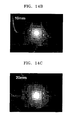
- FIGS. 14A , 14B, and 14C are optical photographs illustrating a brightness difference between three samples with different luminous areas manufactured according to the present invention.
- CNT layers of FIGS. 14A through 14C had diameters of 5 mm (0.19625cm 2 ), 10 mm (0.785cm 2 ), and 20 mm (3.14cm 2 ), respectively.
- FIG. 15 is a graph illustrating results of an electron emission stability test on different types of CNTs. It can be seen from FIG. 15 that MWCNTs are more stable than DWCNTs.
- the afore-described single electron emission source may be applied to a display apparatus.
- display apparatuses have pixels that are electrically addressed in an X-Y matrix, stripe-like cathodes spanning the width of a screen are arranged in parallel, and CNT layers are formed on surfaces of the cathodes to correspond to the pixels.
- FIG. 16 is a plan view illustrating cathodes 31 arranged on a substrate 30 of a display apparatus according to an embodiment of the present invention.
- FIG. 17 is a cross-sectional view taken along line A-A' of FIG. 16 according to an embodiment of the present invention.
- CNT layers 32 are formed on surfaces of the cathodes 31 at intervals corresponding to pitches of pixels of the display apparatus.
- the cathodes 31 are formed of a conductive material or a material with an electrical resistance.
- the cathodes 31 are fixed to the substrate 30 by welding or by using adhesive layers 31 b.
- the CNT layers 32 are fixed to top surfaces of the cathodes 31 by using adhesive layers 31 a formed under the CNT layers 32.
- the adhesive layer 31 a for fixing the CNT layers 32 to the cathodes 31 may be formed on the entire top surfaces of the cathodes 31 as shown in FIG. 16 , or may be formed only under the CNT layers 32.
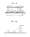
- FIG. 18 is a cross-sectional view of a display apparatus according to an embodiment of the present invention.
- a cathode 31 is attached to a top surface of a substrate 30, which is a rear plate, by using an adhesive layer 31b.
- the adhesive layer 31b fixes the cathode 31 to the substrate 30.
- the adhesive layer 31 b may not used, the cathode 31 may be fixed to the substrate 30 by welding or other adhesion methods.
- a CNT layer 32 is formed on a top surface of the cathode 31.
- the CNT layer 32 is fixed to the cathode 31 by using an adhesive layer 31 a that is formed under the CNT layer 32.
- the cathode 31 is separately manufactured from the substrate 30, and then is fixed to the substrate 30 by using the adhesive layer 31a.
- the CNT layer 32 may be fixed to the cathode 31 in the aforementioned manufacturing method.
- An insulating layer 40 having a through-hole through which the CNT layer 32 is to be passed is formed on the cathode 31, and a grid 41 for extracting electrons is disposed on the insulating layer 40.
- a front plate structure is separately manufactured, and then is integrally coupled to the grid 41.
- the front plate structure includes a front plate 50 and an anode 51 formed on an inner surface of the front plate 50.
- a phosphor layer 52 is formed on a surface of the anode 51.
- the CNT layer 32 disposed on the cathode 31 is manufactured by using a CNT suspension. Since a plurality of CNT layers 32 are disposed on one band-shaped cathode 31, it is necessary to apply a CNT suspension to a plurality of regions of a filter template corresponding to the one cathode 31. To this end, the CNT suspension may be supplied to only the given regions of the cathode 31 by using a printing method or a mask.
- FIG. 19A is a cross-sectional view illustrating a method of manufacturing a cathode of a display apparatus according to an embodiment of the present invention.
- FIG. 19B is a cross-sectional view illustrating a method of manufacturing a cathode of a display apparatus according to another embodiment of the present invention.
- a CNT suspension is supplied to a band-shaped filter template 60 through a nozzle.
- the CNT suspension is dried, and then is transferred, to obtain a cathode 31 having CNT layers 32 as shown in FIGS. 16, 17 , and 18 .
- a suspension may be supplied at one time as shown in FIG. 19B . Referring to FIG.
- a mask 80 having through-holes corresponding to CNT layers is placed over a filter template 60 and then a CNT suspension 32" is supplied. Accordingly, the CNT suspension 32" can be supplied to given regions of the filter template 60 in a short time. In this case, since the CNT suspension 32" is in contact with the mask 80, when the mask 80 is separated from the filter template 60 before the CNT suspension 32" is dried, the CNT suspension 32" is stuck a little to the mask 80, thereby failing to form complete CNT layers on the filter template 60. Accordingly, it is preferable that after the CNT suspension 32" is properly or completely dried, the mask 80 should be separated from the filter template 60. The plurality of CNT layers are formed on the filter template 60 in this way, and then are transferred to the cathode.
- a CNT thin film formed by using a suspension filtering method can be easily transferred by using a conductive tape with strong adhesion. Since adhesion between the CNT thin film and the conductive tape is very high, field electron emission characteristics of the CNT thin film can be improved by a simple taping process. Stable and reliable electric field electron emission characteristics can be obtained without attaching or detaching the CNT thin film during electric field electron emission even at a high electric field.
- the active electron emission site density of the CNT thin film can be easily controlled by controlling the concentration of an evenly dispersed CNT colloidal suspension. Also, a large CNT thin film with uniform characteristics can be easily manufactured by using this method, and thus a large CNT field electron emission source can be manufactured.
- a CNT layer having an optimal concentration for electric field electron emission is formed by preparing an evenly dispersed CNT colloidal suspension by using any of various types of needle-shaped electron emission materials, that is, nanotubes or nanorods having a predetermined length, for example, CNT powder, through a suspension filtering method, supplying the suspension onto a filter template having pores, filtering the suspension through the filter template, and drying the suspension. Since CNTs are very uniformly dispersed in the suspension, the CNT layer formed on the filter template can have uniform CNTs. Since the CNT layer is transferred to a cathode on which an adhesive layer is formed, the CNT layer can be stably fixed to the cathode.
- needle-shaped electron emission materials that is, nanotubes or nanorods having a predetermined length, for example, CNT powder
- the electron emission source according to the present invention can be structurally very stable and can ensure high and uniform electron emission.
- the electron emission source according to the present invention can be simply manufactured at room temperature without a complicated process without using paste including conductive organic/inorganic matters, binders, and polymers which badly affect field electron emission characteristics, a large electron emission source can be manufactured.
- a display apparatus can have one CNT layer at one pixel.
- the concentration of the CNT layer can be easily controlled by controlling the concentration of the CNTs, and accordingly, optimal field electron emission source density can be obtained.
Landscapes
- Engineering & Computer Science (AREA)
- Manufacturing & Machinery (AREA)
- Cold Cathode And The Manufacture (AREA)
- Cathode-Ray Tubes And Fluorescent Screens For Display (AREA)
Claims (8)
- Elektronenemissionsquelle, die Folgendes umfasst:eine leitende, plattenförmige Kathode (11, 31);eine auf einer Oberfläche der Kathode ausgebildete nadelförmige Elektronenemissionsmaterialschicht (13, 32);eine die Kathode tragende Basis (14, 30); undein die Kathode an der Basis befestigendes Befestigungselement (15),dadurch gekennzeichnet, dass eine obere Klebstoffschicht (12, 13a) auf der Oberseite der Kathode ausgebildet ist, um die Emissionsschicht auf die Kathode zu kleben, und eine untere Klebstoffschicht (12a, 31b) auf der Unterseite der Kathode ausgebildet ist, um die Kathode auf die Basis zu kleben.
- Elektronenemissionsquelle nach Anspruch 1, wobei die Kathode einen elektrischen Widerstand hat.
- Elektronenemissionsquelle nach Anspruch 1, wobei ein der nadelförmigen Elektronenemissionsmaterialschicht entsprechender Vorsprung auf der Basis ausgebildet ist und das Befestigungselement ein Befestigungselement ist, das einen Rand der Kathode fest gegen den Vorsprung drückt.
- Elektronenemissionsquelle nach Anspruch 1, wobei das Befestigungselement und die Basis komplementär miteinander im Eingriff sind.
- Verfahren zur Herstellung einer Elektronenemissionsquelle, wobei das Verfahren Folgendes beinhaltet:Aufbringen einer Suspension mit darin dispergierten Elektronenemissionsmaterialien mit Hilfe einer Maske auf eine vorbestimmte Region einer Filterschablone mit Filterfähigkeit; undTrocknen der Suspension zum Bilden einer Elektronenemissionsmaterialschicht (13') auf der Filterschablone;Übertragen der Elektronenemissionsmaterialschicht auf eine plattenförmige oder bandförmige Kathode (11), auf der eine Klebstoffschicht ausgebildet ist; undgekennzeichnet durch Ausführen eines Aufklebevorgangs an der auf die Kathode übertragenenElektronenemissionsmaterialschicht, um Elektronenemissionsmaterialien mit Bezug auf die Kathode aufzustellen, indem ein Aufstellelement mit Haftung am Elektronenemissionsmaterial gegen das Elektronenemissionsmaterial gedrückt und das Aufstellelement von dem Elektronenemissionsmaterial gelöst wird, um das Elektronenemissionsmaterial mit Bezug auf die Kathode aufzustellen.
- Verfahren nach Anspruch 5, wobei das Aufstellelement ein Klebstoffband (22) oder eine Klebstoffrolle (23) ist.
- Anzeigevorrichtung, die Folgendes umfasst:eine Elektronenemissionsquelle nach Anspruch 1, wobei die Basis als Substrat in der Anzeige dient und die Elektronenemissionsmaterialschicht in mehrere Elektronenemissionsmaterialschichten unterteilt ist, die in vorbestimmten Intervallen auf einer Oberseite der Kathode ausgebildet sind;eine von dem Substrat beabstandete Frontplatte;eine Anode, die auf einer Innenfläche der Frontplatte ausgebildet und den Elektronenemissionsmaterialschichten zugewandt ist;eine auf einer Oberfläche der Anode ausgebildete Phosphorschicht; undein Gitter, das zwischen der Kathode und der Phosphorschicht angeordnet ist und Elektronen von den Elektronenemissionsmaterialschichten extrahiert.
- Verfahren zur Herstellung einer Anzeigevorrichtung, die eine Frontplatte, auf der eine Anode ausgebildet ist, und ein Substrat umfasst, auf dem eine Kathode ausgebildet ist, wobei das Verfahren Folgendes beinhaltet:Ausbilden einer Elektronenemissionsquelle mit einem Verfahren gemäß Anspruch 5, das das Ausbilden mehrerer Elektronenemissionsmaterialschichten in vorbestimmten Intervallen auf einer bandförmigen Schablone beinhaltet; undÜbertragen der Elektronenemissionsmaterialschichten zu einer bandförmigen Kathode, auf der eine Klebstoffschicht ausgebildet ist; wobei das Verfahren ferner das Befestigen der Kathode an einer Rückplatte beinhaltet.
Applications Claiming Priority (1)
| Application Number | Priority Date | Filing Date | Title |
|---|---|---|---|
| KR1020080019298A KR100922399B1 (ko) | 2008-02-29 | 2008-02-29 | 전자방출원, 이를 적용한 전자장치 및 전자방출원의제조방법 |
Publications (3)
| Publication Number | Publication Date |
|---|---|
| EP2096659A1 EP2096659A1 (de) | 2009-09-02 |
| EP2096659B1 true EP2096659B1 (de) | 2012-12-26 |
| EP2096659B8 EP2096659B8 (de) | 2013-02-06 |
Family
ID=40602468
Family Applications (1)
| Application Number | Title | Priority Date | Filing Date |
|---|---|---|---|
| EP08157123A Ceased EP2096659B8 (de) | 2008-02-29 | 2008-05-28 | Elektronenemissionsquelle, elektrische Vorrichtung damit und Herstellungsverfahren dafür |
Country Status (4)
| Country | Link |
|---|---|
| US (2) | US8513870B2 (de) |
| EP (1) | EP2096659B8 (de) |
| JP (1) | JP4843001B2 (de) |
| KR (1) | KR100922399B1 (de) |
Families Citing this family (16)
| Publication number | Priority date | Publication date | Assignee | Title |
|---|---|---|---|---|
| KR101126296B1 (ko) * | 2010-04-09 | 2012-03-20 | 한국표준과학연구원 | 탄소나노튜브 시트 제조방법 및 이를 이용한 전계 방출 소자 |
| KR101106121B1 (ko) * | 2010-04-22 | 2012-01-20 | 고려대학교 산학협력단 | 전자 방출원 및 그 제조 방법 |
| WO2011132985A2 (ko) * | 2010-04-22 | 2011-10-27 | 고려대학교 산학협력단 | 전자 방출원 및 그 제조 방법 |
| KR20130101839A (ko) * | 2012-03-06 | 2013-09-16 | 삼성전자주식회사 | 엑스레이 소스 |
| CN103578889B (zh) * | 2012-07-26 | 2015-12-16 | 清华大学 | 碳纳米管场发射体的制备方法 |
| CN103578885B (zh) * | 2012-07-26 | 2016-04-13 | 清华大学 | 碳纳米管场发射体 |
| US9064669B2 (en) * | 2013-07-15 | 2015-06-23 | National Defense University | Field emission cathode and field emission light using the same |
| CN103545158B (zh) * | 2013-10-25 | 2016-03-23 | 中国科学院深圳先进技术研究院 | 碳纳米管阴极及其制备方法 |
| TWI552187B (zh) * | 2014-11-20 | 2016-10-01 | 能資國際股份有限公司 | 冷陰極x射線產生器的封裝結構及其抽真空的方法 |
| US10566170B2 (en) | 2017-09-08 | 2020-02-18 | Electronics And Telecommunications Research Institute | X-ray imaging device and driving method thereof |
| US12350754B2 (en) * | 2017-12-22 | 2025-07-08 | Arcam Ab | Electron beam source and the use of the same |
| CN111115616B (zh) * | 2018-11-01 | 2021-12-03 | 清华大学 | 碳纳米管阵列的表面修复方法 |
| WO2026063251A1 (ja) * | 2024-09-20 | 2026-03-26 | 株式会社明電舎 | 電子源,電子ビーム放出構造,電界放射装置,電子源の製造方法 |
| JP7772162B1 (ja) | 2024-09-20 | 2025-11-18 | 株式会社明電舎 | 電子源の製造方法 |
| JP2026057132A (ja) * | 2024-09-20 | 2026-04-02 | 株式会社明電舎 | 電子源,電子ビーム放出構造,電界放射装置 |
| JP2026057133A (ja) * | 2024-09-20 | 2026-04-02 | 株式会社明電舎 | 電子源,電子ビーム放出構造,電界放射装置 |
Family Cites Families (34)
| Publication number | Priority date | Publication date | Assignee | Title |
|---|---|---|---|---|
| US5789848A (en) * | 1996-08-02 | 1998-08-04 | Motorola, Inc. | Field emission display having a cathode reinforcement member |
| DE69834673T2 (de) * | 1997-09-30 | 2006-10-26 | Noritake Co., Ltd., Nagoya | Verfahren zur Herstellung einer Elektronenemittierenden Quelle |
| EP1059266A3 (de) | 1999-06-11 | 2000-12-20 | Iljin Nanotech Co., Ltd. | Massensyntheseverfahren von hochreinen, auf einem grossformatigem Substrat angeordnete Kohlenstoffnanoröhren mittels thermischer chemischer Dampfphasenabscheidung |
| EP1061554A1 (de) | 1999-06-15 | 2000-12-20 | Iljin Nanotech Co., Ltd. | Weisslichtquelle mit Kohlenstoffnanoröhren und Verfahren zur Herstellung |
| KR100314094B1 (ko) | 1999-08-12 | 2001-11-15 | 김순택 | 전기 영동법을 이용한 카본나노튜브 필드 에미터의 제조 방법 |
| US6277318B1 (en) | 1999-08-18 | 2001-08-21 | Agere Systems Guardian Corp. | Method for fabrication of patterned carbon nanotube films |
| US6590322B2 (en) * | 2000-01-07 | 2003-07-08 | The United States Of America As Represented By The Secretary Of The Navy | Low gate current field emitter cell and array with vertical thin-film-edge emitter |
| EP1256124A1 (de) | 2000-02-16 | 2002-11-13 | Fullerene International Corporation | Diamant-kohlenstoff-nanoröhren-strukturen für effiziente elektronenfeld-emission |
| WO2002041348A1 (en) * | 2000-11-20 | 2002-05-23 | Nec Corporation | Cnt film and field-emission cold cathode comprising the same |
| US6436221B1 (en) * | 2001-02-07 | 2002-08-20 | Industrial Technology Research Institute | Method of improving field emission efficiency for fabricating carbon nanotube field emitters |
| JP2002334649A (ja) * | 2001-03-06 | 2002-11-22 | Nec Kansai Ltd | カソード構体、カソード構体の製造方法およびカラーブラウン管 |
| US7341498B2 (en) * | 2001-06-14 | 2008-03-11 | Hyperion Catalysis International, Inc. | Method of irradiating field emission cathode having nanotubes |
| KR100763890B1 (ko) * | 2001-08-06 | 2007-10-05 | 삼성에스디아이 주식회사 | Cnt를 적용한 전계방출표시소자의 제조방법 |
| KR100805318B1 (ko) * | 2001-09-21 | 2008-02-20 | 삼성에스디아이 주식회사 | 탄소계 물질로 형성된 에미터를 갖는 전계 방출표시소자의 제조 방법 |
| US8062697B2 (en) | 2001-10-19 | 2011-11-22 | Applied Nanotech Holdings, Inc. | Ink jet application for carbon nanotubes |
| JP2003303540A (ja) * | 2002-04-11 | 2003-10-24 | Sony Corp | 電界電子放出膜、電界電子放出電極および電界電子放出表示装置 |
| JP3797299B2 (ja) | 2002-08-30 | 2006-07-12 | 石川島播磨重工業株式会社 | 高電圧用カソード及びその接合方法 |
| JP2004241295A (ja) * | 2003-02-07 | 2004-08-26 | Hitachi Zosen Corp | カーボンナノチューブを用いた電子放出素子用電極材料およびその製造方法 |
| US7150801B2 (en) | 2003-02-26 | 2006-12-19 | Mitsubishi Gas Chemical Company, Inc. | Process for producing cold field-emission cathodes |
| US6969690B2 (en) | 2003-03-21 | 2005-11-29 | The University Of North Carolina At Chapel Hill | Methods and apparatus for patterned deposition of nanostructure-containing materials by self-assembly and related articles |
| CN1310270C (zh) * | 2003-03-26 | 2007-04-11 | 清华大学 | 一种场发射显示器的制备方法 |
| CA2531628A1 (en) * | 2003-07-09 | 2005-02-10 | Hyperion Catalysis International, Inc. | Field emission devices made with laser and/or plasma treated carbon nanotube mats, films or inks |
| TWI276140B (en) * | 2003-09-23 | 2007-03-11 | Ind Tech Res Inst | Method of forming carbon nanotube field emission source |
| KR20050060287A (ko) * | 2003-12-16 | 2005-06-22 | 삼성에스디아이 주식회사 | 카본나노튜브 에미터의 형성방법 |
| US7618300B2 (en) | 2003-12-24 | 2009-11-17 | Duke University | Method of synthesizing small-diameter carbon nanotubes with electron field emission properties |
| US7560134B2 (en) | 2004-06-29 | 2009-07-14 | Applied Nanotech Holdings, Inc. | Nanoparticle implantation |
| KR100642622B1 (ko) | 2005-02-22 | 2006-11-10 | 주식회사 에이엔씨아이 | 탄소나노튜브를 이용한 면상발열체 및 그 제조방법 |
| JP4993642B2 (ja) * | 2005-03-10 | 2012-08-08 | マテリアルズ アンド エレクトロケミカル リサーチ (エムイーアール) コーポレイション | 薄膜製造法および装置 |
| KR100679209B1 (ko) | 2005-06-29 | 2007-02-05 | 이영희 | 얇은 금속층을 이용한 탄소나노튜브 필드 에미터의 제조 방법 |
| KR20070011808A (ko) | 2005-07-21 | 2007-01-25 | 삼성에스디아이 주식회사 | 금속 복합체를 포함한 전자 방출원, 이를 포함한 전자 방출소자 및 상기 전자 방출원 형성용 조성물 |
| CN1959896B (zh) * | 2005-11-04 | 2011-03-30 | 鸿富锦精密工业(深圳)有限公司 | 碳纳米管场发射体及其制备方法 |
| US20070154625A1 (en) * | 2006-01-05 | 2007-07-05 | Teco Electric & Machinery Co., Ltd. | Method for activating electron emission surface of field emission display |
| KR100808631B1 (ko) | 2006-04-21 | 2008-02-29 | 유석용 | 탄소를 발열원으로 하는 발열재의 제조방법 |
| KR100892366B1 (ko) * | 2006-12-26 | 2009-04-10 | 한국과학기술원 | 탄소나노튜브 전계방출 에미터 및 그 제조방법 |
-
2008
- 2008-02-29 KR KR1020080019298A patent/KR100922399B1/ko active Active
- 2008-05-28 EP EP08157123A patent/EP2096659B8/de not_active Ceased
- 2008-05-29 US US12/129,005 patent/US8513870B2/en active Active
- 2008-07-14 JP JP2008183240A patent/JP4843001B2/ja active Active
-
2013
- 2013-07-11 US US13/939,669 patent/US20130295815A1/en not_active Abandoned
Also Published As
| Publication number | Publication date |
|---|---|
| EP2096659A1 (de) | 2009-09-02 |
| US20130295815A1 (en) | 2013-11-07 |
| EP2096659B8 (de) | 2013-02-06 |
| US8513870B2 (en) | 2013-08-20 |
| JP4843001B2 (ja) | 2011-12-21 |
| JP2009212075A (ja) | 2009-09-17 |
| US20090218930A1 (en) | 2009-09-03 |
| KR20090093655A (ko) | 2009-09-02 |
| KR100922399B1 (ko) | 2009-10-19 |
Similar Documents
| Publication | Publication Date | Title |
|---|---|---|
| EP2096659B1 (de) | Elektronenemissionsquelle, elektrische Vorrichtung damit und Herstellungsverfahren dafür | |
| JP4937910B2 (ja) | 電界放出用途のためのカーボンナノチューブの活性化 | |
| US20100181896A1 (en) | Surface field electron emitters using carbon nanotube yarn and method of fabricating carbon nanotube yarn thereof | |
| KR20030059291A (ko) | 카본 나노튜브의 패턴 형성 방법 및 전계 방출형 냉음극과그 제조 방법 | |
| US20100320439A1 (en) | Carbon nanotube structure and method of vertically aligning carbon nanotubes | |
| JP4355928B2 (ja) | 電界放出型冷陰極の製造方法 | |
| KR100977312B1 (ko) | 가요성 전자발광 소자 및 이를 적용한 디스플레이 및 그 제조방법 | |
| JP5055655B2 (ja) | エミッタの製造方法及び該エミッタを用いた電界放出型冷陰極並びに平面画像表示装置 | |
| JP2001312955A (ja) | 電子放出素子、電子放出素子の製造方法、および画像表示素子 | |
| KR101094453B1 (ko) | 전자 방출원의 제조방법 및 이를 적용한 전자소자의 제조방법 | |
| US20100181894A1 (en) | Field electron emitter including nucleic acid-coated carbon nanotube and method of manufacturing the same | |
| JP4770017B2 (ja) | Cnt膜及びその製造方法並びにcnt膜を用いた電界放出型冷陰極及び画像表示装置 | |
| KR100990231B1 (ko) | 전자 방출원의 제조방법 | |
| JP4605425B2 (ja) | 電子放出素子の製造方法 | |
| KR101013604B1 (ko) | 전자 방출원의 제조방법 | |
| JP2007188662A (ja) | 電界放出型冷陰極の製造方法 | |
| KR101046775B1 (ko) | 전자 방출원 | |
| JP5158224B2 (ja) | エミッタの製造方法及び該エミッタを用いた電界放出型冷陰極並びに平面画像表示装置 | |
| KR101151409B1 (ko) | 탄소 나노튜브를 이용한 에미터 제조 방법 및 그 방법으로 제조된 에미터 | |
| KR102878809B1 (ko) | Dc 마그네트론 플라즈마를 이용한 탄소나노튜브 가공 방법, 이를 이용한 전계방출원 | |
| JP4984130B2 (ja) | ナノカーボンエミッタとその製造方法並びに面発光素子 | |
| JP2007323946A (ja) | 冷陰極電子源およびその製造方法 | |
| JP2007149616A (ja) | 電界放出素子とその製造方法 | |
| JP5476751B2 (ja) | ナノカーボンエミッタ及びその製造方法並びにそれを用いた面発光素子 | |
| Lee et al. | P‐154: Optimized Field Emission of Multiwalled Carbon Nantoubes |
Legal Events
| Date | Code | Title | Description |
|---|---|---|---|
| PUAI | Public reference made under article 153(3) epc to a published international application that has entered the european phase |
Free format text: ORIGINAL CODE: 0009012 |
|
| 17P | Request for examination filed |
Effective date: 20080611 |
|
| AK | Designated contracting states |
Kind code of ref document: A1 Designated state(s): AT BE BG CH CY CZ DE DK EE ES FI FR GB GR HR HU IE IS IT LI LT LU LV MC MT NL NO PL PT RO SE SI SK TR |
|
| AX | Request for extension of the european patent |
Extension state: AL BA MK RS |
|
| 17Q | First examination report despatched |
Effective date: 20100330 |
|
| AKX | Designation fees paid |
Designated state(s): DE NL |
|
| GRAP | Despatch of communication of intention to grant a patent |
Free format text: ORIGINAL CODE: EPIDOSNIGR1 |
|
| RIC1 | Information provided on ipc code assigned before grant |
Ipc: H01J 1/304 20060101ALI20120723BHEP Ipc: H01J 31/12 20060101ALI20120723BHEP Ipc: H01J 9/02 20060101AFI20120723BHEP Ipc: C01B 31/02 20060101ALI20120723BHEP |
|
| GRAS | Grant fee paid |
Free format text: ORIGINAL CODE: EPIDOSNIGR3 |
|
| GRAA | (expected) grant |
Free format text: ORIGINAL CODE: 0009210 |
|
| AK | Designated contracting states |
Kind code of ref document: B1 Designated state(s): DE NL |
|
| RAP2 | Party data changed (patent owner data changed or rights of a patent transferred) |
Owner name: KOREA UNIVERSITY INDUSTRIAL & ACADEMIC COLLABORATI |
|
| REG | Reference to a national code |
Ref country code: DE Ref legal event code: R096 Ref document number: 602008021100 Country of ref document: DE Effective date: 20130228 |
|
| REG | Reference to a national code |
Ref country code: NL Ref legal event code: T3 |
|
| PLBE | No opposition filed within time limit |
Free format text: ORIGINAL CODE: 0009261 |
|
| STAA | Information on the status of an ep patent application or granted ep patent |
Free format text: STATUS: NO OPPOSITION FILED WITHIN TIME LIMIT |
|
| 26N | No opposition filed |
Effective date: 20130927 |
|
| REG | Reference to a national code |
Ref country code: DE Ref legal event code: R097 Ref document number: 602008021100 Country of ref document: DE Effective date: 20130927 |
|
| PGFP | Annual fee paid to national office [announced via postgrant information from national office to epo] |
Ref country code: DE Payment date: 20210406 Year of fee payment: 14 |
|
| PGFP | Annual fee paid to national office [announced via postgrant information from national office to epo] |
Ref country code: NL Payment date: 20210406 Year of fee payment: 14 |
|
| REG | Reference to a national code |
Ref country code: DE Ref legal event code: R119 Ref document number: 602008021100 Country of ref document: DE |
|
| REG | Reference to a national code |
Ref country code: NL Ref legal event code: MM Effective date: 20220601 |
|
| PG25 | Lapsed in a contracting state [announced via postgrant information from national office to epo] |
Ref country code: DE Free format text: LAPSE BECAUSE OF NON-PAYMENT OF DUE FEES Effective date: 20221201 |
|
| PG25 | Lapsed in a contracting state [announced via postgrant information from national office to epo] |
Ref country code: NL Free format text: LAPSE BECAUSE OF NON-PAYMENT OF DUE FEES Effective date: 20220601 |