EP2096672A2 - Elektronische Schnittstelle im Mischmaßstab und Herstellungsverfahren - Google Patents
Elektronische Schnittstelle im Mischmaßstab und Herstellungsverfahren Download PDFInfo
- Publication number
- EP2096672A2 EP2096672A2 EP09006878A EP09006878A EP2096672A2 EP 2096672 A2 EP2096672 A2 EP 2096672A2 EP 09006878 A EP09006878 A EP 09006878A EP 09006878 A EP09006878 A EP 09006878A EP 2096672 A2 EP2096672 A2 EP 2096672A2
- Authority
- EP
- European Patent Office
- Prior art keywords
- layer
- nanoscale
- pad
- microscale
- sub
- Prior art date
- Legal status (The legal status is an assumption and is not a legal conclusion. Google has not performed a legal analysis and makes no representation as to the accuracy of the status listed.)
- Granted
Links
- 238000000034 method Methods 0.000 title claims description 35
- 238000004519 manufacturing process Methods 0.000 title description 13
- 239000002070 nanowire Substances 0.000 claims abstract description 149
- 239000000463 material Substances 0.000 claims description 12
- 239000000758 substrate Substances 0.000 claims description 12
- 239000004020 conductor Substances 0.000 claims description 9
- RTAQQCXQSZGOHL-UHFFFAOYSA-N Titanium Chemical compound [Ti] RTAQQCXQSZGOHL-UHFFFAOYSA-N 0.000 claims description 7
- 239000010936 titanium Substances 0.000 claims description 6
- 229910052719 titanium Inorganic materials 0.000 claims description 6
- 238000005530 etching Methods 0.000 claims description 3
- 238000000151 deposition Methods 0.000 claims description 2
- 239000003989 dielectric material Substances 0.000 claims description 2
- 239000010410 layer Substances 0.000 description 178
- 235000005205 Pinus Nutrition 0.000 description 26
- 241000218602 Pinus <genus> Species 0.000 description 26
- 230000008569 process Effects 0.000 description 10
- VYPSYNLAJGMNEJ-UHFFFAOYSA-N Silicium dioxide Chemical compound O=[Si]=O VYPSYNLAJGMNEJ-UHFFFAOYSA-N 0.000 description 8
- 230000008520 organization Effects 0.000 description 7
- 238000013459 approach Methods 0.000 description 5
- 230000007547 defect Effects 0.000 description 5
- 230000002950 deficient Effects 0.000 description 5
- 238000000926 separation method Methods 0.000 description 5
- 238000012360 testing method Methods 0.000 description 5
- 238000012544 monitoring process Methods 0.000 description 4
- BASFCYQUMIYNBI-UHFFFAOYSA-N platinum Chemical compound [Pt] BASFCYQUMIYNBI-UHFFFAOYSA-N 0.000 description 4
- 239000000377 silicon dioxide Substances 0.000 description 4
- 229910052681 coesite Inorganic materials 0.000 description 3
- 229910052906 cristobalite Inorganic materials 0.000 description 3
- 238000013461 design Methods 0.000 description 3
- 238000012986 modification Methods 0.000 description 3
- 230000004048 modification Effects 0.000 description 3
- 229910052682 stishovite Inorganic materials 0.000 description 3
- 229910052905 tridymite Inorganic materials 0.000 description 3
- 230000006399 behavior Effects 0.000 description 2
- AOJOEFVRHOZDFN-UHFFFAOYSA-N benzyl 2-methylprop-2-enoate Chemical compound CC(=C)C(=O)OCC1=CC=CC=C1 AOJOEFVRHOZDFN-UHFFFAOYSA-N 0.000 description 2
- 230000007423 decrease Effects 0.000 description 2
- 230000002349 favourable effect Effects 0.000 description 2
- 238000005457 optimization Methods 0.000 description 2
- 238000000059 patterning Methods 0.000 description 2
- 238000000206 photolithography Methods 0.000 description 2
- 229910052697 platinum Inorganic materials 0.000 description 2
- 239000004926 polymethyl methacrylate Substances 0.000 description 2
- 238000011160 research Methods 0.000 description 2
- 239000000126 substance Substances 0.000 description 2
- 230000007704 transition Effects 0.000 description 2
- JBRZTFJDHDCESZ-UHFFFAOYSA-N AsGa Chemical compound [As]#[Ga] JBRZTFJDHDCESZ-UHFFFAOYSA-N 0.000 description 1
- SOGAXMICEFXMKE-UHFFFAOYSA-N Butylmethacrylate Chemical compound CCCCOC(=O)C(C)=C SOGAXMICEFXMKE-UHFFFAOYSA-N 0.000 description 1
- 229910001218 Gallium arsenide Inorganic materials 0.000 description 1
- 239000000956 alloy Substances 0.000 description 1
- JJWKPURADFRFRB-UHFFFAOYSA-N carbonyl sulfide Chemical compound O=C=S JJWKPURADFRFRB-UHFFFAOYSA-N 0.000 description 1
- 229920001940 conductive polymer Polymers 0.000 description 1
- 230000003247 decreasing effect Effects 0.000 description 1
- 230000001934 delay Effects 0.000 description 1
- 230000008021 deposition Effects 0.000 description 1
- 230000002542 deteriorative effect Effects 0.000 description 1
- 229910003460 diamond Inorganic materials 0.000 description 1
- 239000010432 diamond Substances 0.000 description 1
- 238000010894 electron beam technology Methods 0.000 description 1
- 230000007613 environmental effect Effects 0.000 description 1
- 230000003993 interaction Effects 0.000 description 1
- 238000005297 material degradation process Methods 0.000 description 1
- 229910052751 metal Inorganic materials 0.000 description 1
- 229910001092 metal group alloy Inorganic materials 0.000 description 1
- 238000004377 microelectronic Methods 0.000 description 1
- 238000005498 polishing Methods 0.000 description 1
- 229920001490 poly(butyl methacrylate) polymer Polymers 0.000 description 1
- 229920003229 poly(methyl methacrylate) Polymers 0.000 description 1
- 239000011241 protective layer Substances 0.000 description 1
- 230000008439 repair process Effects 0.000 description 1
- 238000012827 research and development Methods 0.000 description 1
- 238000001338 self-assembly Methods 0.000 description 1
- 229910052710 silicon Inorganic materials 0.000 description 1
- 239000010703 silicon Substances 0.000 description 1
- 235000012239 silicon dioxide Nutrition 0.000 description 1
- 230000003068 static effect Effects 0.000 description 1
- 230000001052 transient effect Effects 0.000 description 1
- 238000009966 trimming Methods 0.000 description 1
- 238000011144 upstream manufacturing Methods 0.000 description 1
Images


Classifications
-
- H—ELECTRICITY
- H10—SEMICONDUCTOR DEVICES; ELECTRIC SOLID-STATE DEVICES NOT OTHERWISE PROVIDED FOR
- H10D—INORGANIC ELECTRIC SEMICONDUCTOR DEVICES
- H10D84/00—Integrated devices formed in or on semiconductor substrates that comprise only semiconducting layers, e.g. on Si wafers or on GaAs-on-Si wafers
- H10D84/01—Manufacture or treatment
-
- H—ELECTRICITY
- H10—SEMICONDUCTOR DEVICES; ELECTRIC SOLID-STATE DEVICES NOT OTHERWISE PROVIDED FOR
- H10D—INORGANIC ELECTRIC SEMICONDUCTOR DEVICES
- H10D62/00—Semiconductor bodies, or regions thereof, of devices having potential barriers
- H10D62/10—Shapes, relative sizes or dispositions of the regions of the semiconductor bodies; Shapes of the semiconductor bodies
- H10D62/117—Shapes of semiconductor bodies
- H10D62/118—Nanostructure semiconductor bodies
-
- B—PERFORMING OPERATIONS; TRANSPORTING
- B82—NANOTECHNOLOGY
- B82Y—SPECIFIC USES OR APPLICATIONS OF NANOSTRUCTURES; MEASUREMENT OR ANALYSIS OF NANOSTRUCTURES; MANUFACTURE OR TREATMENT OF NANOSTRUCTURES
- B82Y10/00—Nanotechnology for information processing, storage or transmission, e.g. quantum computing or single electron logic
-
- H—ELECTRICITY
- H10—SEMICONDUCTOR DEVICES; ELECTRIC SOLID-STATE DEVICES NOT OTHERWISE PROVIDED FOR
- H10D—INORGANIC ELECTRIC SEMICONDUCTOR DEVICES
- H10D62/00—Semiconductor bodies, or regions thereof, of devices having potential barriers
- H10D62/10—Shapes, relative sizes or dispositions of the regions of the semiconductor bodies; Shapes of the semiconductor bodies
- H10D62/117—Shapes of semiconductor bodies
- H10D62/118—Nanostructure semiconductor bodies
- H10D62/119—Nanowire, nanosheet or nanotube semiconductor bodies
- H10D62/121—Nanowire, nanosheet or nanotube semiconductor bodies oriented parallel to substrates
-
- H—ELECTRICITY
- H10—SEMICONDUCTOR DEVICES; ELECTRIC SOLID-STATE DEVICES NOT OTHERWISE PROVIDED FOR
- H10D—INORGANIC ELECTRIC SEMICONDUCTOR DEVICES
- H10D62/00—Semiconductor bodies, or regions thereof, of devices having potential barriers
- H10D62/10—Shapes, relative sizes or dispositions of the regions of the semiconductor bodies; Shapes of the semiconductor bodies
- H10D62/117—Shapes of semiconductor bodies
- H10D62/118—Nanostructure semiconductor bodies
- H10D62/119—Nanowire, nanosheet or nanotube semiconductor bodies
- H10D62/122—Nanowire, nanosheet or nanotube semiconductor bodies oriented at angles to substrates, e.g. perpendicular to substrates
-
- H—ELECTRICITY
- H10—SEMICONDUCTOR DEVICES; ELECTRIC SOLID-STATE DEVICES NOT OTHERWISE PROVIDED FOR
- H10K—ORGANIC ELECTRIC SOLID-STATE DEVICES
- H10K19/00—Integrated devices, or assemblies of multiple devices, comprising at least one organic element specially adapted for rectifying, amplifying, oscillating or switching, covered by group H10K10/00
- H10K19/202—Integrated devices comprising a common active layer
-
- B—PERFORMING OPERATIONS; TRANSPORTING
- B82—NANOTECHNOLOGY
- B82Y—SPECIFIC USES OR APPLICATIONS OF NANOSTRUCTURES; MEASUREMENT OR ANALYSIS OF NANOSTRUCTURES; MANUFACTURE OR TREATMENT OF NANOSTRUCTURES
- B82Y40/00—Manufacture or treatment of nanostructures
-
- G—PHYSICS
- G11—INFORMATION STORAGE
- G11C—STATIC STORES
- G11C2213/00—Indexing scheme relating to G11C13/00 for features not covered by this group
- G11C2213/70—Resistive array aspects
- G11C2213/81—Array wherein the array conductors, e.g. word lines, bit lines, are made of nanowires
-
- H—ELECTRICITY
- H01—ELECTRIC ELEMENTS
- H01H—ELECTRIC SWITCHES; RELAYS; SELECTORS; EMERGENCY PROTECTIVE DEVICES
- H01H1/00—Contacts
- H01H1/0094—Switches making use of nanoelectromechanical systems [NEMS]
-
- H—ELECTRICITY
- H10—SEMICONDUCTOR DEVICES; ELECTRIC SOLID-STATE DEVICES NOT OTHERWISE PROVIDED FOR
- H10K—ORGANIC ELECTRIC SOLID-STATE DEVICES
- H10K10/00—Organic devices specially adapted for rectifying, amplifying, oscillating or switching; Organic capacitors or resistors having potential barriers
- H10K10/50—Bistable switching devices
-
- H—ELECTRICITY
- H10—SEMICONDUCTOR DEVICES; ELECTRIC SOLID-STATE DEVICES NOT OTHERWISE PROVIDED FOR
- H10K—ORGANIC ELECTRIC SOLID-STATE DEVICES
- H10K10/00—Organic devices specially adapted for rectifying, amplifying, oscillating or switching; Organic capacitors or resistors having potential barriers
- H10K10/701—Organic molecular electronic devices
Definitions
- the present invention is related to integrated circuits and other electronic devices and, in particular, to a mixed-scale interface suitable for densely interconnecting nanoscale electronics with microscale electronics within an integrated circuit or other electronic device.
- nanowire crossbars comprising multiple layers of parallel nanowires are fabricated by self-assembly or self-orientation with molecular-scale widths on surfaces.
- the grid-like nanowire crossbars provide a two-dimensional array of nanowire junctions at the closest points of contact between nanowires of a first layer, oriented in a first direction, and nanowires of a second layer, oriented in a second direction approximately perpendicular to the first direction.
- the nanowire junctions comprising a small number of molecules of a nanonwire-junction substance, can be fabricated to have properties of resistors, diodes, transistors, and other familiar components of conventional electronic circuits.
- nanoscale electronic circuits Many different prototype nanoscale electronic circuits have been produced in research and development environments, and continued research efforts are producing palettes of nanoscale-electronic components and features of increasing sizes, a rich variety of useful nanoscale-electronic component organizations, and a variety of fabrication methods for producing nanoscale electronic components and devices.
- practical, commercial electronic devices need to include large scale, microscale, and submicroscale components and circuits that interface to nanoscale electronic devices and circuitry.
- devising reliable and cost-effective interfaces between microscale and submicroscale electronics and nanoscale electronics has proven to be more difficult than the design and fabrication of nanoscale electronic devices.
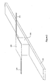
- Figure 1 illustrates an exemplary demultiplexer/nanowire-crossbar configuration that allows individual nanowire junctions within a nanowire crossbar to be accessed by address signals input to microscale signal lines.
- a first demultiplexer 102 interconnects a small number of microscale address signal lines 104 to a much larger number of parallel nanowires 106 within a nanowire crossbar 108.
- a second demultiplexer 110 interconnects a second set of microscale address signal lines 112 to a second set of parallel nanowires 114 within the nanowire crossbar 108.
- Various nanowire junctions may be configured to have particular electronic properties, including properties characteristic of transistors, resistors, diodes, and other such electronic components, represented in Figure 1 with filled circles, such as filled circle 116, overlying particular nanowire junctions.
- the four address lines e.g. address lines 104
- the demultiplexer can carry any of 2 4 or 16 different digital patterns, or addresses, of high and low voltage or current binary signals on each address line.
- the demultiplexer can translate each different perceived address into a pattern of high and low signals output to the nanowires to which it is connected.
- a demultiplexer outputs a high, or Boolean "1,” signal to a single nanowire corresponding to a four-bit nanowire address received through the microscale address signal lines, and low, or Boolean "0" signals to the remaining, non-addressed nanowires.
- each nanowire junction within the nanowire crossbar can be individually addressed by a pair of addresses, one address received on the first set of address signal lines 104 and a second address received on the second set of address signal lines 112.
- the nanowire crossbar can be configured arbitrarily to implement any of a large number of different possible circuits which output result signals to selected nanowires.
- the nanowire crossbar in Figure 1 is exemplary of the overall organization, and is not intended to represent any particular circuit or device.
- demultiplexer-based microscale/nanoscale interfaces have been developed, and the demultiplexer-based microscale/nanoscale interface has been shown to be a feasible and effective nanoscale/microscale interface technique.
- addressing of a single nanowire by each multiplexer at each instant in time represents a significant bandwidth constriction since, as shown in the example shown in Figure 1 , only one junction may be addressed at a time.
- Demultiplexer-based nanoscale/microscale interfaces may therefore represent significant bandwidth bottlenecks within mixed-scale microelectronic devices.
- the demultiplexer-based approach may additionally add design and fabrication overheads, cost, and reliability problems to mixed-scale electronic devices with densely interconnected microscale and nanoscale circuits and functional modules. Therefore, researchers and developers of mixed-scale electronic devices continue to seek more reliable, more easily fabricated, and less bandwidth-constricting nanoscale/microscale interfaces for use in mixed-scale electronic devices.
- Embodiments of the present invention are directed to mixed-scale electronic interfaces, included in integrated circuits and other electronic devices, that provide for dense electrical interconnection between microscale features of a predominantly microscale or submicroscale layer and nanoscale features of a predominantly nanoscale layer.
- the predominantly nanoscale layer in one embodiment of the present invention, comprises a tessellated pattern of submicroscale or microscale pads densely interconnected by nanowire junctions between sets of parallel, closely spaced nanowire bundles.
- the predominantly submicroscale or microscale layer includes pins positioned complementarily to the submicroscale or microscale pads in the predominantly nanoscale layer. More complex mixed-scale electronic interfaces that include two or more microscale or submicroscale layers and/or two or more nanoscale layers can also be designed and fabricated according to methods of the present invention.
- Embodiments of the present invention are directed to nanoscale/microscale interfaces that permit dense interconnections between microscale and submicroscale features and logic and nanoscale features and logic within an integrated circuit or other electronic device.
- nanoscale refers to features and components with a least one dimension smaller than 100 nanometers.
- nanoscale may refer to features and components with at least one dimension smaller than 50 nanometers, and, in certain cases, less than 10 nanometers.
- submicroscale generally refers to features and components with at least on dimension smaller than 1 micron
- microscale refers to features and components with dimensions equal to, or greater than, 1 micron.
- microscale and submicroscale features and components can be fabricated by conventional photolithographic techniques, but nanoscale components and features can generally be fabricated, currently, using nanoimprint techniques or other non-photolithographic techniques.
- a described nanoscale/microscale-interface embodiment of the present invention interconnects pads in a predominantly nanoscale layer with correspondingly regularly patterned microscale or submicroscale pins in a predominantly submicroscale or microscale layer.
- Each pad in the predominantly nanoscale layer may be interconnected through nanowire-junctions with a large number of neighboring pads through nanowire junctions in lattice-like channels of nanowires.
- a pad within the predominantly nanoscale layer can be accessed by conventional submicroscale or microscale electronics in the second, predominantly microscale or submicroscale layer via a submicroscale or microscale pin.
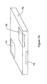
- Figure 2 illustrates a single pin/pad interface within a two-layer nanoscale/macroscale-interface embodiment of the present invention.
- a submicroscale or microscale pin 202 connects to a submicroscale or microscale signal line 204.
- the pin 202 and signal line 204 are both embedded within the predominantly submicroscale or microscale layer of the two-layer nanoscale/microscale-interface embodiment of the present invention.
- the pin 202 also electrically contacts a pad 206 that is, in turn, interconnected with a first nanowire 208 and a second nanowire 210.
- PINU pad-interconnected-nanowire unit
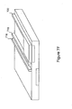
- Figure 3 illustrates, in the same fashion as Figure 2 , two pad/pin interfaces within a nanoscale/macroscale-interface embodiment of the present invention.
- a first microscale or submicroscale signal line 302 electrically contacts a first pin 304.
- the first pin also electrically contacts the pad 306 of a first PINU 307.
- the first PINU 307 resides in a first sub-layer of the predominantly nanoscale layer of the nanoscale/macroscale interface.
- a second submicroscale or microscale signal line 308 electrically contacts a second pin 310.
- the second pin also electrically contacts the pad 312 of a second PINU 313.
- the second PINU 313 resides within a second sub-layer of the predominantly nanoscale layer of the two-layer nanoscale/macroscale interface.
- Two nanowires 314 and 316 of the two PINUs 307 and 313 intersect at a nanowire junction 318, which, like the nanowire junctions in nanowire crossbars, may comprise one or a small number of molecules that implement a passive or active nanoscale electrical component, such as a resistor, a variable-resistance resistor, a diode, a transistor, or other passive or active component.
- a passive or active nanoscale electrical component such as a resistor, a variable-resistance resistor, a diode, a transistor, or other passive or active component.
- pairs of pins of the predominantly microscale layer of a two-layer nanoscale/microscale interface are electrically interconnected via a pair of PINUs and a single nanowire junction.
- the predominantly microscale and submicroscale layer may implement various types of logic and functional units, and the predominantly nanoscale layer may serve primarily to interconnect the various submicroscale or microscale components and logic.
- Figures 4A-D illustrate the overall organization and patterning of one class of two-layer nanoscale/macroscale-interface embodiments of the present invention.
- the predominantly submicroscale or microscale layer of the two-layer nanoscale/microscale interface can be considered to be organized into square or rectangular cells to form a rectilinear grid of microscale cells.
- Figure 4A shows a tiny portion of the predominantly microscale layer of a two-layer nanoscale/macroscale interface that includes 30 microscale cells, such as microscale cell 402.
- the rectilinear organization of the predominantly microscale layer reflects only the arrangements of submicroscale or microscale pins within the predominantly microscale layer.
- each microscale cell contains a small number of submicroscale or microscale pins that are identically arranged and positioned in each microscale cell of the rectilinear grid.
- two-pin cells are illustrated.
- four-pin microscale cells are employed. Because the pins are identically arranged in each microscale cell, the pins also form a regular pattern across the surface of the predominantly microscale layer.
- Figure 4B shows the organization of pad-interconnected-nanowire units ("PINUs") within a small portion of a first sub-layer of the predominantly nanoscale layer of a two-layer nanoscale/macroscale-interface embodiment of the present invention.
- the PINUs are arranged so that the centers of the pads of the PINUs fall on linear columns and rows.
- a horizontal dashed line 402 is drawn through the centers of pads in one row
- a vertical dashed line 404 is drawn through the centers of a column of pads.
- the PINUs, including both the pad-portion and nanowire-portions of each PINU, are rotated by a small angle ⁇ (406 in Figure 4B ) with respect to the row direction.
- Rotation of the PINUs allows nanowires of the PINUs to form closely spaced nanowire bundles, such as closely spaced nanowire bundle 408 in Figure 4B , oriented at the small angle ⁇ with respect to the row direction.
- the rows and columns that define the center of the PINUs form a rectilinear grid with square cells, although, in alternative embodiments, the columns need not be perpendicular to the rows, and the cells may be rhomboid.
- the centers of the pads of the first nanoscale sub-layer are positioned to directly overlie the centers of approximately one-half of the pins in the predominantly microscale layer of the two-layer nanoscale/microscale interface, with the remaining pins centered within each square nanoscale cell of the first nanoscale sub-layer.
- Figure 4C shows a second nanoscale sub-layer overlaying the first nanoscale sub-layer shown in Figure 4B to form a small portion of the tessellated, predominately nanoscale layer of a two-layer nanoscale/macroscale-interface embodiment of the present invention.
- the second nanoscale sub-layer is identical in organization to the first nanoscale sub-layer, but is rotated 90 degrees with respect to the first nanoscale sub-layer and translated, by 1/ ⁇ 2 times the pad-repeat distance along columns and rows of the first nanoscale sub-layer, in a diagonal direction, so that the pads of the second nanoscale sub-layer are located at the centers of the cells formed by the pads of the first nanoscale sub-layer and so that each second-sub-layer pad is, in the case of square cells, equidistant from the nearest surrounding pads of the first nanoscale sub-layer.
- the nanowires of the second nanoscale sub-layer form parallel, closely spaced bundles, such as parallel, closely spaced bundle 410, perpendicular to the parallel, closely spaced bundles of nanowires of the first nanoscale sub-layer.
- each of the two nanowires of each PINU has a length equal to approximately three times the repeat distance of pads in the column and row directions of the nanoscale sub-layer that contains the PINU.
- nanowire 412 emanating from pad 414 of the second nanoscale sub-layer spans pads 416-418 of the first nanoscale sub-layer, which have pad-repeat distances equal to those in the second nanoscale sub-layer.
- the nanowires may have much greater lengths with respect to the pad repeat distance, as long as a nanowire in one layer is not positioned so closely to a pin or pad in the other layer that there is an undesired electrical interaction between the two.
- Pad 414 is representative of the vast majority of pads within a large, predominantly nanoscale layer of the illustrated two-layer nanoscale/microscale interface, and is surrounded by two vertical and two horizontal channels, each comprising parallel, closely spaced bundles having a three-nanowire width, which separate pad 414 from its four nearest neighbor pads 420-423 in the first nanoscale sub-layer.
- Figure 4D illustrates, in a fashion similar to Figures 4B and 4C , a tessellated, predominantly nanoscale layer of a two-layer nanoscale/microscale-interface embodiment of the present invention in which each of the two nanowires of each PINU have a length equal to approximately four times the repeat distance of the pads within the nanoscale sub-layer that contains the PINU. While, in Figure 4C , the parallel, closely spaced bundles of nanowires each includes, at each point, three separate nanowires, in the parallel, closely spaced bundles of nanowires in Figure 4D each includes, at each point, up to four nanowires.
- each channel is actually composed of many different nanowires, since channels span the entire, or a large portion of the, predominantly nanoscale layer, while individual nanowires are generally much shorter.
- the length of the nanowires of each PINU determine the width, in nanowires, of the parallel, closely spaced bundles of nanowires, or channels, within the tessellated, predominantly nanoscale layer.
- the darkly colored pads, such as pad 426 lie in a first nanoscale sub-layer
- the lighter shaded pads, such as pad 428 lie in a second nanoscale sub-layer.
- Figure 5 illustrates the first-nanoscale-sub-layer pads potentially electrically connected, through a single nanowire junction, to one particular second-nanoscale-sub-layer pad in the tessellated, predominantly nanoscale layer of a two-layer nanoscale/microscale interface-embodiment of the present invention shown in Figure 4D .
- the nanowires 501 and 502 emanating from the particular second-nanoscale-sub-layer pad 506 each span four pad-repeat distances.
- Each of the two nanowires 501 and 502 therefore cross over, and form nanowire junctions, with the four nanowires in eight different channels.
- nanowire 502 forms nanowire junctions with each of the four nanowires in channels 508-515.
- Each nanowire junction potentially connects, depending on the nature of the nanowire junction, the nanowire with a first-nanoscale-layer PINU.
- the particular second-nanoscale-sub-layer pad 506 may be electrically interconnected with the 64 first-nanoscale-level pads, such as first-nanoscale-sub-layer pad 516, shown in Figure 5 , and numbered 1-64.
- a single pin of the predominantly microscale or submicroscale layer of the two-layer nanoscale/microscale interface may therefore be connected, in the embodiment illustrated in Figure 4D , to each of up to 64 neighboring pins by two PINUs and a single intervening nanowire junction.
- a given pad or pin may be electrically interconnected, through single nanowire junctions, with up to 400 neighboring pins or pads.
- a tessellated, predominantly nanoscale layer that may be used in a two-layer nanoscale/microscale interface according to the present invention.
- pad-repeat distances may vary, angles between rows and columns of pads may depart from 90°, and pad-cornered cells of the tessellated, predominantly nanoscale layer may be, in addition to squares and rectangles, diamond shaped or rhomboid in nature.
- pad-cornered cells of the tessellated, predominantly nanoscale layer may be, in addition to squares and rectangles, diamond shaped or rhomboid in nature.
- PINUs there are a number of other symmetry-related arrangements with equivalent pad spacings and column and row orientations.
- Figure 6 illustrates four symmetry-related arrangements 602, 604, 606, and 608 of a first-nanoscale-sub-layer pad and a second-nanoscale-sub-layer pad within a tessellated, predominantly nanoscale layer of a two-layer nanoscale/microscale-interface embodiment of the present invention.
- a much larger number of symmetry related arrangements for any given arrangement may be possible.
- Figures 7A-T illustrate one method for fabricating a two-layer nanoscale/microscale-interface embodiment of the present invention, the method constituting an additional embodiment of the present invention.
- the process begins with a substrate consisting of, or including, a predominantly microscale layer 702 with a regular arrangement of microscale or submicroscale pins 704 and 706 at the surface of the substrate.
- the pins may be composed of a variety of conductive materials, including conductive polymers, metal elements or alloys, or conductive and doped silicon or gallium arsenide, and may be embedded in a variety of different substrate materials, including silicon dioxide.
- the predominantly microscale layer 702 includes further submicroscale or microscale components, signal lines, and other features 704 that implement various functional components and logic elements of an electronic device.
- the predominantly microscale layer is fabricated using conventional photolithographic methods.
- nanoimprint resist 708 such as solvated poly-methyl-methacrylate (“PMMA”) or poly-benzyl-methacrylate (“PBMA”) dissolved in benzyl-methacrylate
- PMMA solvated poly-methyl-methacrylate
- PBMA poly-benzyl-methacrylate
- the nanoimprint resist may be cured and then imprinted by a nanoimprinting technique to form troughs 710-712 and basins 714 corresponding to first-nanoscale-sub-layer nanowires and pads, respectively.
- Nanoimprinting techniques generally employ nanoimprinting stamps prepared from masters fabricated by painstaking, electron-beam-based techniques.
- the nanoimprinted nascent nanoscale/microscale interface may be briefly exposed to a nanoimprint-resist etchant to remove nanoimprint resist from the floors of the nanoimprinted troughs and basins.
- a conductive layer 716 is deposited above the nanoimprint resist to form first-nanoscale-sub-layer PINUs.
- platinum is used for PINUs.
- Unwanted portions of the deposited, conductive layer and underlying nanoimprint resist may be subsequently removed by a lift-off process to produce well-formed, conductive PINUs, as shown in Figure 7F .
- a two-step process may be used to first remove unwanted conductive material, as shown in Figure 7E , and to then remove nanoimprint resist. Any remaining nanoimprint resist may be removed by exposing the nascent two-layer nanoscale/microscale interface to a nanoimprint-resist etchant. At this point, the first-nanoscale-sub-layer PINUs 718-720 are fully fabricated.
- This dielectric layer may be polished by a chemical/mechanical polishing step.
- a nanoimprint resist layer 732 is applied.
- basins 734 are imprinted, in a second nanoimprinting step, over microscale-layer pads that are not yet overlain with nanoscale PINU pads.
- an etching step may then be performed to etch through the SiO 2 layer to expose the microscale-layer pad underlying the nanoimprinted basins.
- a conductive layer 736 is next applied, and a liftoff process or two-step nanoimprint/conductive-layer removal process can then be used to produce a modified, first-nanoscale-sub-layer with conductive pillars, or vias 738, that rise up from the underlying microscale-layer pads to the surface of the modified, first-nanoscale-sub-layer.
- nanowire-junction material 740 is next deposited on the surface of the nascent two-layer nanoscale/microscale interface.
- the nanowire-junction material may be, in certain embodiments, a variably resistive material that can reversibly transition between a relatively high conductivity state and a relatively low conductivity state upon application of two different voltages. Such material allows nanowire junctions to be configured electronically to either electrically interconnect the two nanowires that cross at the nanowire junction or to electrically isolate the two nanowires from one another.
- alternative types of nanowire-junction materials may be deposited to produce alternative types of nanowire-junction components.
- multiple layers may be deposited in order to produce multi-layer nanowire junctions.
- a thin layer of titanium 742 is deposited on the surface of the nascent two-layer nanoscale/microscale interface.
- a second layer of nanoimprint resist 744 is deposited on the surface of the nascent two-layer nanoscale/microscale interface and cured.
- a third nanoimprinting step as shown in Figure 7P , the nanoimprint resist is stamped to produce troughs 747-749 and basins 750 in which second-nanoscale-layer nanowires and pads are subsequently formed.
- a second layer of conductive material 752 is deposited on the surface of the nascent two-layer nanoscale/microscale interface, the conductive material forming the PINUs of the second nanoscale sub-layer.
- platinum is again used for the second-sub-layer PINUs.
- Unwanted portions of the conductive layer and underlying nanoimprint resist are then removed by a second lift-off process, as shown in Figure 7R , to produce a surface with exposed, second-nanoscale-level PINUs lying above a titanium coated surface.
- the nascent two-layer nanoscale/microscale interface can be etched to remove all non-PINU material down to the substrate surface, with nanowire-junction material and titanium remaining only below the second-nanoscale layer PINUs, where the nanowire-junction material and titanium layers are shielded from the etching process. This results in production of the two-layer nanoscale/microscale interface 754 shown in Figure 7S .
- an additional SiO 2 layer may be applied, and polished, to produce a final two-layer nanoscale/microscale interface 756.
- the two-layer nanoscale/microscale interface may be additionally coated with protective layers or additional device layers, as needed for a particular application.
- a two-layer nanoscale/microscale interface of the present invention can be characterized by a number of different parameters. Moreover, various embodiments of the present invention can be optimized for particular applications by optimizing one or more of these parameters with respect to various different criteria.
- One characterizing parameter is the angle ⁇ by which PINUs are rotated with respect to a linear row of pad centers within a nanoscale sub-layer.
- Figure 8 shows a rectilinear grid 802 of square microscale cells, such as microscale cell 804, each cell containing two different microscale pins, such as microscale pins 806-807 in microscale cell 804.
- the rectilinear grid 802 in Figure 8 represents the predominantly microscale layer of a two-layer nanoscale/microscale interface above which the tessellated, predominantly nanoscale layer is fabricated.
- the angle ⁇ may be chosen to optimize the two-layer nanoscale/microscale interface.
- the numerous arrows emanating from pin 808, such as arrow 810, in Figure 8 represent a few of the many choices for the angle ⁇ with respect to the direction of the rows of pins within the rectilinear grid 802.
- a characteristic parameter of the two-layer nanoscale/microscale interface is a minimum distance of separation between a nanowire and any microscale pin other than the microscale pin on which the pad of the PINU including the nanowire is centered.
- the maximum possible lengths of the nanowires emanating from a PINU positioned over pin 808 vary with ⁇ .
- the nanowire would need to be relatively short, to avoid coming within a distance less than a minimum separation distance to any neighboring pin, such as neighboring pin 812.
- Approach of a nanowire to a neighboring microscale pin closer than a threshold minimum distance may result in a short within the predominantly nanoscale layer.
- certain values of ⁇ corresponding to the directions represented by arrows 810, 814, 816, and 818 are clearly more favorable than others, including those corresponding to the direction represented by arrow 812.
- the ⁇ angles represented by arrows 810 and 818 correspond to the most favorable directions.
- the angle ⁇ may be selected to be as close as possible to the direction indicated by arrow 818 in Figure 8 .
- each PINU has equal-length nanowires.
- Equal length nanowires are not required, but may be desirable for minimizing reactive-capacitance delays within the predominantly nanoscale layer for a particular degree of pin interconnection.
- the greater symmetry provided by equal-length nanowires may, in many applications, also facilitate routing of signals between microscale pins.
- Another characteristic parameter for two-layer nanoscale/microscale interfaces of the present invention is the dimensions of PINU pads.
- PINU pads In general, when the area of the pads is relatively small, a greater fraction of the area of the nanoscale layer can be devoted to nanowires and nanowire interconnections.
- Additional parameters include a minimal distance of separation between nanowires, the width of nanowires, dimensions of the microscale-layer pins, dimensions of the repeating units, or cells, that define the interface between the microscale and nanoscale layers, a minimum distance of separation between nanowires and pins, and parameters that characterize uncertainties and errors in alignment of the nanoscale layer to the microscale layer and in the positioning of features within each layer.
- Nanowire junctions can be fabricated within the nanoscale layer of a nanoscale/microscale interface.
- Bistable junctions can be used as conventional switches. It is also possible to fabricate nanowire junctions that behave as diodes, transistors, variable resistors, and that exhibit even more exotic behaviors and characteristics without analogs in microscale devices.
- Such a diverse palette of components types allows for implementation of digital and analog logic in the nanoscale layer, as well as self-modifying tuning and defect-compensating functionality that provides the nanoscale/microscale interface with an ability to be configured following manufacture and to configure itself, over time, to optimize performance and to compensate for defects.
- a circuit with sufficient built-in logic may monitor its performance and correctness of operation in order to work around defects that inevitably arise over time due to environmental and operational hazards, such as cosmic rays, material degradation, static charges, and transient voltage pulses.
- variable-resistor-like nanowire junctions can be used to trim an integrated circuit. Resistance values for various variable-resistor nanowire junctions can be selected, for example, to adjust internal voltages to compensate for variances in other components and features of a circuit above tolerance thresholds that would otherwise cause the circuit to exhibit undesired behavior and characteristics or to completely fail. For example, a defective switch may transition from one state to another between 3 and 4 volts, instead of between 0 volts and 2 volts, resulting in the switch being stuck in only one state despite input voltages that vary between 0V and 2V, to which the defective switch was designed to respond. By trimming an upstream variable-resistance nanowire junction to a lower resistance value, the input voltages to the switch may be adjusted from between 0V and 2V to between 3V and 4V, so that the switch is appropriately responsive to the input voltages.
- configurable nanowire junctions may be used to shunt signals from a defective logic module to a redundant, equivalent module or to a newly configured, replacement module, in order to isolate the defective module.
- Test or monitor logic within an integrated circuit may, using spare cycles and resource, periodically or continuously monitor an integrated circuit to detect and compensate for defective or functionally deteriorating components and features, and to configure replacement components and features.
- While monitor and repair of an integrated circuit can increase manufacturing yields and extend the useful lifetimes of integrated circuits, optimization logic within a mixed-scale-interface embodiment of the present invention may lead to more highly customized and operationally efficient integrated circuits, tuned to specific applications, than could be economically designed and manufactured by volume manufacturing processes.
- an integrated circuit may recognize and optimize operational patterns and heavily used functionality by reconfiguring itself to more efficiently carry out often repeated tasks, much like particular software routines may be specifically optimized and tuned beyond initial encoding produced by compilers from high-level languages.
- the electronic devices within which integrated circuits are used may themselves contain defects, or develop defects or degrade, over time, and a mixed-scale-interface embodiment of the present invention may reconfigure itself to compensate for such external defects and inefficiencies, either as a result of feedback provided by external testing and monitoring functionality, or by application-specific monitoring and testing logic configured into the mixed-scale interface in a post-manufacturing configuration process.
- Nanoscale layers of a mixed-scale interface provide for sufficient redundancy of interconnection and components, as well as stable, but reconfigurable components and features, to allow for effective and comprehensive post-manufacturing tuning, adjustment, and reconfiguration needed for self-modifying defect-compensating and optimization functionalities that can significantly improve manufacturing yields, application-specific customization, and useful lifetimes of integrated circuits.
- nanoscale/microscale-interface embodiments of the present invention can be fabricated using any of many different fabrication methods to produce nanoscale/microscale interfaces with different characteristics, including different orientation angles of PINUs with respect to the microscale-cell-grid row directions, different microscale-cell grid geometries and dimensions, different nanoscale-layer patterns and spacing, different PINU dimensions, and other such characteristics.
- 4-nanowire PINUs may be arranged in a regular, rectilinear array within the predominantly nanoscale layer of a nanoscale/microscale-interface.
- 3-nanowire PINUs may be arranged in a hexagonal tiling patterns.
- different types of PINUs may be combined to create more complex tilings with a variety of different symmetries.
Landscapes
- Engineering & Computer Science (AREA)
- Chemical & Material Sciences (AREA)
- Nanotechnology (AREA)
- Physics & Mathematics (AREA)
- Mathematical Physics (AREA)
- Theoretical Computer Science (AREA)
- Crystallography & Structural Chemistry (AREA)
- Semiconductor Integrated Circuits (AREA)
- Internal Circuitry In Semiconductor Integrated Circuit Devices (AREA)
- Semiconductor Memories (AREA)
- Exposure Of Semiconductors, Excluding Electron Or Ion Beam Exposure (AREA)
Applications Claiming Priority (2)
| Application Number | Priority Date | Filing Date | Title |
|---|---|---|---|
| US11/342,076 US7544977B2 (en) | 2006-01-27 | 2006-01-27 | Mixed-scale electronic interface |
| EP07709841A EP1977427B1 (de) | 2006-01-27 | 2007-01-26 | Mischskalige elektronische schnittstelle |
Related Parent Applications (2)
| Application Number | Title | Priority Date | Filing Date |
|---|---|---|---|
| EP07709841A Division EP1977427B1 (de) | 2006-01-27 | 2007-01-26 | Mischskalige elektronische schnittstelle |
| EP07709841.6 Division | 2007-01-26 |
Publications (3)
| Publication Number | Publication Date |
|---|---|
| EP2096672A2 true EP2096672A2 (de) | 2009-09-02 |
| EP2096672A3 EP2096672A3 (de) | 2010-01-13 |
| EP2096672B1 EP2096672B1 (de) | 2011-08-03 |
Family
ID=38080870
Family Applications (2)
| Application Number | Title | Priority Date | Filing Date |
|---|---|---|---|
| EP09006878A Ceased EP2096672B1 (de) | 2006-01-27 | 2007-01-26 | Elektronische Schnittstelle im Mischmaßstab und Herstellungsverfahren |
| EP07709841A Ceased EP1977427B1 (de) | 2006-01-27 | 2007-01-26 | Mischskalige elektronische schnittstelle |
Family Applications After (1)
| Application Number | Title | Priority Date | Filing Date |
|---|---|---|---|
| EP07709841A Ceased EP1977427B1 (de) | 2006-01-27 | 2007-01-26 | Mischskalige elektronische schnittstelle |
Country Status (7)
| Country | Link |
|---|---|
| US (3) | US7544977B2 (de) |
| EP (2) | EP2096672B1 (de) |
| JP (1) | JP4995837B2 (de) |
| KR (1) | KR101099988B1 (de) |
| CN (1) | CN101375344B (de) |
| DE (1) | DE602007005098D1 (de) |
| WO (1) | WO2007089522A1 (de) |
Families Citing this family (38)
| Publication number | Priority date | Publication date | Assignee | Title |
|---|---|---|---|---|
| US7671398B2 (en) * | 2005-02-23 | 2010-03-02 | Tran Bao Q | Nano memory, light, energy, antenna and strand-based systems and methods |
| US7741204B2 (en) * | 2006-10-30 | 2010-06-22 | Hewlett-Packard Development Company, L.P. | Mixed-scale electronic interfaces |
| US8835831B2 (en) | 2010-06-22 | 2014-09-16 | Zena Technologies, Inc. | Polarized light detecting device and fabrication methods of the same |
| US8507840B2 (en) | 2010-12-21 | 2013-08-13 | Zena Technologies, Inc. | Vertically structured passive pixel arrays and methods for fabricating the same |
| US8519379B2 (en) * | 2009-12-08 | 2013-08-27 | Zena Technologies, Inc. | Nanowire structured photodiode with a surrounding epitaxially grown P or N layer |
| US8889455B2 (en) | 2009-12-08 | 2014-11-18 | Zena Technologies, Inc. | Manufacturing nanowire photo-detector grown on a back-side illuminated image sensor |
| US8384007B2 (en) | 2009-10-07 | 2013-02-26 | Zena Technologies, Inc. | Nano wire based passive pixel image sensor |
| US8890271B2 (en) | 2010-06-30 | 2014-11-18 | Zena Technologies, Inc. | Silicon nitride light pipes for image sensors |
| US8299472B2 (en) | 2009-12-08 | 2012-10-30 | Young-June Yu | Active pixel sensor with nanowire structured photodetectors |
| US8269985B2 (en) | 2009-05-26 | 2012-09-18 | Zena Technologies, Inc. | Determination of optimal diameters for nanowires |
| US9406709B2 (en) | 2010-06-22 | 2016-08-02 | President And Fellows Of Harvard College | Methods for fabricating and using nanowires |
| US8866065B2 (en) | 2010-12-13 | 2014-10-21 | Zena Technologies, Inc. | Nanowire arrays comprising fluorescent nanowires |
| US9082673B2 (en) | 2009-10-05 | 2015-07-14 | Zena Technologies, Inc. | Passivated upstanding nanostructures and methods of making the same |
| US9478685B2 (en) | 2014-06-23 | 2016-10-25 | Zena Technologies, Inc. | Vertical pillar structured infrared detector and fabrication method for the same |
| US8274039B2 (en) | 2008-11-13 | 2012-09-25 | Zena Technologies, Inc. | Vertical waveguides with various functionality on integrated circuits |
| US20110115041A1 (en) * | 2009-11-19 | 2011-05-19 | Zena Technologies, Inc. | Nanowire core-shell light pipes |
| US9000353B2 (en) | 2010-06-22 | 2015-04-07 | President And Fellows Of Harvard College | Light absorption and filtering properties of vertically oriented semiconductor nano wires |
| US8735797B2 (en) | 2009-12-08 | 2014-05-27 | Zena Technologies, Inc. | Nanowire photo-detector grown on a back-side illuminated image sensor |
| US8748799B2 (en) | 2010-12-14 | 2014-06-10 | Zena Technologies, Inc. | Full color single pixel including doublet or quadruplet si nanowires for image sensors |
| US8791470B2 (en) | 2009-10-05 | 2014-07-29 | Zena Technologies, Inc. | Nano structured LEDs |
| US9515218B2 (en) | 2008-09-04 | 2016-12-06 | Zena Technologies, Inc. | Vertical pillar structured photovoltaic devices with mirrors and optical claddings |
| US8546742B2 (en) * | 2009-06-04 | 2013-10-01 | Zena Technologies, Inc. | Array of nanowires in a single cavity with anti-reflective coating on substrate |
| US9343490B2 (en) | 2013-08-09 | 2016-05-17 | Zena Technologies, Inc. | Nanowire structured color filter arrays and fabrication method of the same |
| US9299866B2 (en) | 2010-12-30 | 2016-03-29 | Zena Technologies, Inc. | Nanowire array based solar energy harvesting device |
| US8229255B2 (en) | 2008-09-04 | 2012-07-24 | Zena Technologies, Inc. | Optical waveguides in image sensors |
| US8114787B2 (en) | 2009-02-19 | 2012-02-14 | Empire Technology Development Llc | Integrated circuit nanowires |
| US7969774B2 (en) * | 2009-03-10 | 2011-06-28 | Micron Technology, Inc. | Electronic devices formed of two or more substrates bonded together, electronic systems comprising electronic devices and methods of making electronic devices |
| WO2011133144A1 (en) | 2010-04-20 | 2011-10-27 | Hewlett-Packard Development Company, L.P. | A self-arranging, luminescence-enhancement device for surface-enhanced luminescence |
| WO2012015443A1 (en) | 2010-07-30 | 2012-02-02 | Hewlett-Packard Development Company, L.P. | Optical fiber surface enhanced raman spectroscopy (sers) probe |
| WO2012054027A1 (en) | 2010-10-20 | 2012-04-26 | Hewlett-Packard Development Company, L.P. | Chemical-analysis device integrated with metallic-nanofinger device for chemical sensing |
| US9274058B2 (en) | 2010-10-20 | 2016-03-01 | Hewlett-Packard Development Company, L.P. | Metallic-nanofinger device for chemical sensing |
| US9310306B2 (en) | 2011-02-17 | 2016-04-12 | Hewlett-Packard Development Company, L.P. | Apparatus for use in sensing applications |
| US8593629B2 (en) | 2011-02-17 | 2013-11-26 | Hewlett-Packard Development Company, L.P. | Apparatus for performing SERS |
| US9377409B2 (en) | 2011-07-29 | 2016-06-28 | Hewlett-Packard Development Company, L.P. | Fabricating an apparatus for use in a sensing application |
| US8520202B2 (en) | 2011-09-15 | 2013-08-27 | Hewlett-Packard Development Company, L.P. | Asymmetrical-nanofinger device for surface-enhanced luminescense |
| US8605281B2 (en) | 2011-10-13 | 2013-12-10 | Hewlett-Packard Development Company, L.P. | Probe having nano-fingers |
| CN112669714B (zh) * | 2020-12-22 | 2022-09-20 | 业成科技(成都)有限公司 | 发光二极体显示器及其制作方法 |
| US11742295B2 (en) * | 2020-12-28 | 2023-08-29 | Global Unichip Corporation | Interface of integrated circuit die and method for arranging interface thereof |
Citations (2)
| Publication number | Priority date | Publication date | Assignee | Title |
|---|---|---|---|---|
| US4486705A (en) | 1981-01-16 | 1984-12-04 | Burroughs Corporation | Method of testing networks on a wafer having grounding points on its periphery |
| EP1484644A2 (de) | 2003-06-02 | 2004-12-08 | Hewlett-Packard Development Company, L.P. | Form, Anordnung von Nanoleitungen, Multiplexer/Demultiplexer und dessen Herstellung |
Family Cites Families (11)
| Publication number | Priority date | Publication date | Assignee | Title |
|---|---|---|---|---|
| SE8104574L (sv) * | 1981-07-28 | 1983-01-29 | Svenska Flaektfabriken Ab | Styranordning for en elektrostatisk stoftavskiljare |
| JP2001284572A (ja) * | 2000-03-29 | 2001-10-12 | Hewlett Packard Co <Hp> | 電子デバイス |
| JP2002289621A (ja) * | 2001-03-27 | 2002-10-04 | Japan Science & Technology Corp | ナノメータースケール素子の配線接続方法及びその評価方法とそのための配線接続装置及びその評価装置 |
| US7073157B2 (en) | 2002-01-18 | 2006-07-04 | California Institute Of Technology | Array-based architecture for molecular electronics |
| DE60313462T2 (de) * | 2002-07-25 | 2008-01-03 | California Institute Of Technology, Pasadena | Sublithographische nanobereichs-speicherarchitektur |
| DE10259634B4 (de) * | 2002-12-18 | 2008-02-21 | Qimonda Ag | Verfahren zur Herstellung von Kontakten auf einem Wafer |
| US6774004B1 (en) * | 2003-03-17 | 2004-08-10 | Sharp Laboratories Of America, Inc. | Nano-scale resistance cross-point memory array |
| US7191380B2 (en) * | 2003-09-10 | 2007-03-13 | Hewlett-Packard Development Company, L.P. | Defect-tolerant and fault-tolerant circuit interconnections |
| US7327037B2 (en) * | 2004-04-01 | 2008-02-05 | Lucent Technologies Inc. | High density nanostructured interconnection |
| US7307271B2 (en) * | 2004-11-05 | 2007-12-11 | Hewlett-Packard Development Company, L.P. | Nanowire interconnection and nano-scale device applications |
| JP4496094B2 (ja) * | 2005-01-14 | 2010-07-07 | シャープ株式会社 | 半導体装置及び半導体集積回路 |
-
2006
- 2006-01-27 US US11/342,076 patent/US7544977B2/en active Active
-
2007
- 2007-01-26 EP EP09006878A patent/EP2096672B1/de not_active Ceased
- 2007-01-26 KR KR1020087018510A patent/KR101099988B1/ko not_active Expired - Fee Related
- 2007-01-26 JP JP2008552399A patent/JP4995837B2/ja not_active Expired - Fee Related
- 2007-01-26 CN CN2007800036302A patent/CN101375344B/zh not_active Expired - Fee Related
- 2007-01-26 WO PCT/US2007/001988 patent/WO2007089522A1/en not_active Ceased
- 2007-01-26 DE DE602007005098T patent/DE602007005098D1/de active Active
- 2007-01-26 EP EP07709841A patent/EP1977427B1/de not_active Ceased
- 2007-01-31 US US11/701,086 patent/US7692215B2/en not_active Expired - Fee Related
-
2009
- 2009-12-03 US US12/630,076 patent/US7833842B2/en not_active Expired - Fee Related
Patent Citations (2)
| Publication number | Priority date | Publication date | Assignee | Title |
|---|---|---|---|---|
| US4486705A (en) | 1981-01-16 | 1984-12-04 | Burroughs Corporation | Method of testing networks on a wafer having grounding points on its periphery |
| EP1484644A2 (de) | 2003-06-02 | 2004-12-08 | Hewlett-Packard Development Company, L.P. | Form, Anordnung von Nanoleitungen, Multiplexer/Demultiplexer und dessen Herstellung |
Also Published As
| Publication number | Publication date |
|---|---|
| KR101099988B1 (ko) | 2011-12-28 |
| US20100081238A1 (en) | 2010-04-01 |
| US20070205483A1 (en) | 2007-09-06 |
| CN101375344A (zh) | 2009-02-25 |
| US7692215B2 (en) | 2010-04-06 |
| EP2096672A3 (de) | 2010-01-13 |
| KR20080094011A (ko) | 2008-10-22 |
| US20070176168A1 (en) | 2007-08-02 |
| WO2007089522A1 (en) | 2007-08-09 |
| US7544977B2 (en) | 2009-06-09 |
| US7833842B2 (en) | 2010-11-16 |
| JP2009525193A (ja) | 2009-07-09 |
| JP4995837B2 (ja) | 2012-08-08 |
| EP2096672B1 (de) | 2011-08-03 |
| DE602007005098D1 (de) | 2010-04-15 |
| CN101375344B (zh) | 2012-04-04 |
| EP1977427A1 (de) | 2008-10-08 |
| EP1977427B1 (de) | 2010-03-03 |
Similar Documents
| Publication | Publication Date | Title |
|---|---|---|
| EP2096672B1 (de) | Elektronische Schnittstelle im Mischmaßstab und Herstellungsverfahren | |
| Stan et al. | Molecular electronics: From devices and interconnect to circuits and architecture | |
| Snider et al. | Nano/CMOS architectures using a field-programmable nanowire interconnect | |
| KR101409310B1 (ko) | 3차원 크로스바 어레이 접합에 저장된 정보를 판독 및 기록하기 위한 3차원 크로스바 어레이 시스템 및 방법 | |
| US7922919B2 (en) | Crossbar-array designs and wire addressing methods that tolerate misalignment of electrical components at wire overlap points | |
| US6256767B1 (en) | Demultiplexer for a molecular wire crossbar network (MWCN DEMUX) | |
| KR102536213B1 (ko) | 반도체 장치 | |
| US20040150010A1 (en) | Molecular-junction-nanowire-crossbar-based neural network | |
| CN101292300B (zh) | 纳米级移位寄存器和使用微米级/纳米级移位寄存器的信号解复用 | |
| US8773882B2 (en) | Mixed-scale electronic interfaces | |
| US8390323B2 (en) | Dense nanoscale logic circuitry | |
| US7211503B2 (en) | Electronic devices fabricated by use of random connections | |
| EP2504856B1 (de) | Verfahren zur Herstellung von Interconnects in integrierten Schaltungen mit planaren elektronischen Bauelementen | |
| US7307345B2 (en) | Crossbar-array designs and wire addressing methods that tolerate misalignment of electrical components at wire overlap points | |
| Rachlin et al. | Analysis of mask-based nanowire decoders | |
| US7228518B2 (en) | Method for reducing the size and nanowire length used in nanowire crossbars without reducing the number of nanowire junctions | |
| KR102874942B1 (ko) | 전력 그리드 구조물을 포함하는 반도체 디바이스 및 제조 방법 | |
| DeHon | Architecture approaching the atomic scale | |
| US7517794B2 (en) | Method for fabricating nanoscale features | |
| CN118039584A (zh) | 半导体器件及其制造方法 | |
| HK1137163A1 (en) | Memory elements and cross point switches and arrays of same using nonvolatile nanotube blocks | |
| HK1137163B (en) | Memory elements and cross point switches and arrays of same using nonvolatile nanotube blocks |
Legal Events
| Date | Code | Title | Description |
|---|---|---|---|
| PUAI | Public reference made under article 153(3) epc to a published international application that has entered the european phase |
Free format text: ORIGINAL CODE: 0009012 |
|
| 17P | Request for examination filed |
Effective date: 20090522 |
|
| AC | Divisional application: reference to earlier application |
Ref document number: 1977427 Country of ref document: EP Kind code of ref document: P |
|
| AK | Designated contracting states |
Kind code of ref document: A2 Designated state(s): DE FR GB |
|
| PUAL | Search report despatched |
Free format text: ORIGINAL CODE: 0009013 |
|
| AK | Designated contracting states |
Kind code of ref document: A3 Designated state(s): DE FR GB |
|
| 17Q | First examination report despatched |
Effective date: 20100315 |
|
| RIC1 | Information provided on ipc code assigned before grant |
Ipc: H01L 27/00 20060101AFI20101006BHEP |
|
| GRAJ | Information related to disapproval of communication of intention to grant by the applicant or resumption of examination proceedings by the epo deleted |
Free format text: ORIGINAL CODE: EPIDOSDIGR1 |
|
| GRAP | Despatch of communication of intention to grant a patent |
Free format text: ORIGINAL CODE: EPIDOSNIGR1 |
|
| GRAP | Despatch of communication of intention to grant a patent |
Free format text: ORIGINAL CODE: EPIDOSNIGR1 |
|
| RAP1 | Party data changed (applicant data changed or rights of an application transferred) |
Owner name: HEWLETT-PACKARD DEVELOPMENT COMPANY, L.P. |
|
| GRAS | Grant fee paid |
Free format text: ORIGINAL CODE: EPIDOSNIGR3 |
|
| GRAA | (expected) grant |
Free format text: ORIGINAL CODE: 0009210 |
|
| AC | Divisional application: reference to earlier application |
Ref document number: 1977427 Country of ref document: EP Kind code of ref document: P |
|
| AK | Designated contracting states |
Kind code of ref document: B1 Designated state(s): DE FR GB |
|
| REG | Reference to a national code |
Ref country code: GB Ref legal event code: FG4D |
|
| REG | Reference to a national code |
Ref country code: DE Ref legal event code: R096 Ref document number: 602007016329 Country of ref document: DE Effective date: 20111006 |
|
| REG | Reference to a national code |
Ref country code: DE Ref legal event code: R081 Ref document number: 602007016329 Country of ref document: DE Owner name: HEWLETT-PACKARD DEVELOPMENT COMPANY, L.P., US Free format text: FORMER OWNER: HEWLETT-PACKARD DEVELOPMENT COMPANY, L.P., HOUSTON, US Effective date: 20110907 Ref country code: DE Ref legal event code: R081 Ref document number: 602007016329 Country of ref document: DE Owner name: HEWLETT-PACKARD DEVELOPMENT COMPANY, L.P., HOU, US Free format text: FORMER OWNER: HEWLETT-PACKARD DEVELOPMENT COMPANY, L.P., HOUSTON, TEX., US Effective date: 20110907 Ref country code: DE Ref legal event code: R081 Ref document number: 602007016329 Country of ref document: DE Owner name: HEWLETT PACKARD ENTERPRISE DEVELOPMENT LP, HOU, US Free format text: FORMER OWNER: HEWLETT-PACKARD DEVELOPMENT COMPANY, L.P., HOUSTON, TEX., US Effective date: 20110907 |
|
| PLBE | No opposition filed within time limit |
Free format text: ORIGINAL CODE: 0009261 |
|
| STAA | Information on the status of an ep patent application or granted ep patent |
Free format text: STATUS: NO OPPOSITION FILED WITHIN TIME LIMIT |
|
| 26N | No opposition filed |
Effective date: 20120504 |
|
| REG | Reference to a national code |
Ref country code: DE Ref legal event code: R097 Ref document number: 602007016329 Country of ref document: DE Effective date: 20120504 |
|
| REG | Reference to a national code |
Ref country code: FR Ref legal event code: PLFP Year of fee payment: 10 |
|
| REG | Reference to a national code |
Ref country code: DE Ref legal event code: R082 Ref document number: 602007016329 Country of ref document: DE Representative=s name: SCHOPPE, ZIMMERMANN, STOECKELER, ZINKLER, SCHE, DE Ref country code: DE Ref legal event code: R081 Ref document number: 602007016329 Country of ref document: DE Owner name: HEWLETT PACKARD ENTERPRISE DEVELOPMENT LP, HOU, US Free format text: FORMER OWNER: HEWLETT-PACKARD DEVELOPMENT COMPANY, L.P., HOUSTON, TEX., US |
|
| REG | Reference to a national code |
Ref country code: GB Ref legal event code: 732E Free format text: REGISTERED BETWEEN 20160818 AND 20160824 |
|
| REG | Reference to a national code |
Ref country code: FR Ref legal event code: TP Owner name: HEWLETT PACKARD ENTREPRISE DEVELOPMENT LP, US Effective date: 20160819 |
|
| REG | Reference to a national code |
Ref country code: FR Ref legal event code: PLFP Year of fee payment: 11 |
|
| REG | Reference to a national code |
Ref country code: FR Ref legal event code: PLFP Year of fee payment: 12 |
|
| PGFP | Annual fee paid to national office [announced via postgrant information from national office to epo] |
Ref country code: FR Payment date: 20201217 Year of fee payment: 15 Ref country code: GB Payment date: 20201218 Year of fee payment: 15 |
|
| PGFP | Annual fee paid to national office [announced via postgrant information from national office to epo] |
Ref country code: DE Payment date: 20201217 Year of fee payment: 15 |
|
| REG | Reference to a national code |
Ref country code: DE Ref legal event code: R119 Ref document number: 602007016329 Country of ref document: DE |
|
| GBPC | Gb: european patent ceased through non-payment of renewal fee |
Effective date: 20220126 |
|
| PG25 | Lapsed in a contracting state [announced via postgrant information from national office to epo] |
Ref country code: GB Free format text: LAPSE BECAUSE OF NON-PAYMENT OF DUE FEES Effective date: 20220126 Ref country code: DE Free format text: LAPSE BECAUSE OF NON-PAYMENT OF DUE FEES Effective date: 20220802 |
|
| PG25 | Lapsed in a contracting state [announced via postgrant information from national office to epo] |
Ref country code: FR Free format text: LAPSE BECAUSE OF NON-PAYMENT OF DUE FEES Effective date: 20220131 |
|
| REG | Reference to a national code |
Ref country code: DE Ref legal event code: R081 Ref document number: 602007016329 Country of ref document: DE Owner name: HEWLETT PACKARD ENTERPRISE DEVELOPMENT LP, SPR, US Free format text: FORMER OWNER: HEWLETT PACKARD ENTERPRISE DEVELOPMENT LP, HOUSTON, TEX., US Ref country code: DE Ref legal event code: R082 Ref document number: 602007016329 Country of ref document: DE Representative=s name: HL KEMPNER PATENTANWALT, RECHTSANWALT, SOLICIT, DE |