EP2096818A2 - Procédé et système pour étalonner des modulateurs de quadrature - Google Patents
Procédé et système pour étalonner des modulateurs de quadrature Download PDFInfo
- Publication number
- EP2096818A2 EP2096818A2 EP09153929A EP09153929A EP2096818A2 EP 2096818 A2 EP2096818 A2 EP 2096818A2 EP 09153929 A EP09153929 A EP 09153929A EP 09153929 A EP09153929 A EP 09153929A EP 2096818 A2 EP2096818 A2 EP 2096818A2
- Authority
- EP
- European Patent Office
- Prior art keywords
- phase
- signals
- compensation
- partial
- calculating
- Prior art date
- Legal status (The legal status is an assumption and is not a legal conclusion. Google has not performed a legal analysis and makes no representation as to the accuracy of the status listed.)
- Withdrawn
Links
- 238000000034 method Methods 0.000 title claims abstract description 47
- 238000012360 testing method Methods 0.000 claims abstract description 79
- 238000004590 computer program Methods 0.000 claims description 3
- 230000000694 effects Effects 0.000 description 19
- 239000000243 solution Substances 0.000 description 18
- 230000005540 biological transmission Effects 0.000 description 7
- 230000008569 process Effects 0.000 description 7
- 239000008186 active pharmaceutical agent Substances 0.000 description 5
- 238000013459 approach Methods 0.000 description 4
- 230000010363 phase shift Effects 0.000 description 4
- 239000011159 matrix material Substances 0.000 description 3
- 230000006978 adaptation Effects 0.000 description 2
- 230000004075 alteration Effects 0.000 description 1
- 238000004364 calculation method Methods 0.000 description 1
- 239000012482 calibration solution Substances 0.000 description 1
- 230000015556 catabolic process Effects 0.000 description 1
- 230000001413 cellular effect Effects 0.000 description 1
- 238000006243 chemical reaction Methods 0.000 description 1
- 125000004122 cyclic group Chemical group 0.000 description 1
- 238000006731 degradation reaction Methods 0.000 description 1
- 230000001419 dependent effect Effects 0.000 description 1
- 238000013461 design Methods 0.000 description 1
- 230000001627 detrimental effect Effects 0.000 description 1
- 230000003292 diminished effect Effects 0.000 description 1
- 238000001914 filtration Methods 0.000 description 1
- 238000012986 modification Methods 0.000 description 1
- 230000004048 modification Effects 0.000 description 1
- 230000009467 reduction Effects 0.000 description 1
- 238000006467 substitution reaction Methods 0.000 description 1
- 238000012546 transfer Methods 0.000 description 1
Images



Classifications
-
- H—ELECTRICITY
- H04—ELECTRIC COMMUNICATION TECHNIQUE
- H04L—TRANSMISSION OF DIGITAL INFORMATION, e.g. TELEGRAPHIC COMMUNICATION
- H04L27/00—Modulated-carrier systems
- H04L27/32—Carrier systems characterised by combinations of two or more of the types covered by groups H04L27/02, H04L27/10, H04L27/18 or H04L27/26
- H04L27/34—Amplitude- and phase-modulated carrier systems, e.g. quadrature-amplitude modulated carrier systems
Definitions
- the solution according to an embodiment of the present invention relates to the telecommunication field. More particularly, this solution relates to the calibration of transmitter apparatuses.
- Modem wireless telecommunication systems need to guarantee transmissions with data transfer rates as high as possible; at the same time, they need to be designed in such a way to be cost-effective and to require low power consumptions.
- homodyne systems are based on a so-called direct conversion method, according to which a receiver directly converts the received signals from a carrier Radio Frequency (RF) to a base-band frequency.
- RF Radio Frequency
- homodyne systems allow avoiding the use of expensive intermediate-frequency filters, which are instead required in the heterodyne architectures.
- a quadrature transmitter usually includes one or more quadrature modulators, which receive two base-band signals to be transmitted and generate a corresponding modulated signal. More particularly, the base-band signals are brought to the RF domain used for the transmission by properly modulating them with a corresponding carrier wave, so that the resulting signals are in quadrature to each other; then, the signals in quadrature are mixed together to form the modulated signal.
- the base-band signals of a typical quadrature homodyne architecture may be generated exploiting the so-called Orthogonal Frequency-Division Multiplexing (OFDM) technique, which is a particular digital modulation scheme that makes use of a large number of closely-spaced sinusoidal waves; alternatively, the base band signals may by generated by filtering Binary Phase-Shift Keying (BPSK) sequences using Nyquist shapes or by exploiting other known techniques.
- OFDM Orthogonal Frequency-Division Multiplexing
- BPSK Binary Phase-Shift Keying
- a possible solution is of pre-compensating the base-band signals to be modulated so as to counterbalance the gain and phase errors; for this purpose a proper compensation is applied to the base-band signals, which compensation is quantified according to an estimate of the gain and phase errors.
- the document " New Methods for Adaptation of Quadrature Modulators and Demodulators in Amplifier Linearization Circuits " by J. K. Cavers discloses a method for compensating the gain and phase errors of quadrature modulators, which method make uses of a closed feedback measure loop.
- the method provides for feeding the quadrature modulator with a base-band test signal, which is modulated to obtain a corresponding RF signal; then, the RF signal is provided to an envelope detector, in such a way to obtain an indication of the gain and phase errors generated by the imperfections of the modulator.
- the output of the modulator is phase-dependant, since it depends on the test signal; thus the method requires the exact knowledge of a measure of the loop's delay, which is usually not available.
- An alternative solution provided by the method consists of the transmission of a dc tone in the base-band and then in the performing of measures with a "step and measure" technique. This last operation cannot be easily performed in OFDM systems, since the dc tone - corresponding to the frequency of the carrier - is usually removed by the circuits adapted to couple the base-band section with the RF section.
- an aspect of the solution according to an embodiment of the invention proposes a calibration method for reducing modulation errors in a telecommunication transmitter apparatus.
- the calibration method includes the step of providing a plurality of pairs of test signals; the test signals of each pair are substantially in quadrature to each other, and the pairs of test signals are at least in part different with all the pairs of test signals that have a substantially equal energy.
- the method further includes the steps of generating a plurality of modulated signals, with each modulated signal that is generated by modulating a corresponding pair of test signals; calculating a plurality of transformed signals each one corresponding to the square of a corresponding modulated signal in the frequency domain; and calculating a plurality of partial error indicators each one as a function of the modulus of a corresponding transformed signal.
- the partial error indicators are indicative of the modulation errors associated with the modulated signals.
- the method still further includes the steps of calculating a compensation for counterbalancing the modulation errors according to a combination of the partial error indicators and storing an indication of the compensation for the application of the compensation to each further pair of operative signals during operation of the telecommunication transmitter apparatus.
- the step of generating the modulated signals includes modulating the test signals of each pair with a carrier wave, and obtaining each modulated signal by combining the corresponding modulated test signals.
- the step of calculating the transformed signals includes calculating a Fourier transform of each squared signal.
- each modulation error includes a phase error indicative of an undesired phase offset between the modulated signals and a gain error indicative of an undesired amplitude offset between the modulated signals; the step of calculating the compensation includes calculating a phase compensation for counterbalancing the phase error and a gain compensation for counterbalancing the gain error.
- each offset indicator includes a first offset indicator term equal to the cosine of twice an offset angle and a second indicator term equal to the sine of twice the offset angle
- each pair of test signals includes a first test signal having an amplitude that is proportional to the cosine of the offset angle and a second test signal having an amplitude that is proportional to the sine of the offset angle
- the second test signal has a phase that differs from a phase of the corresponding first test signal in the pair by 90 degrees.
- the step of generating the partial compensations includes (for each partial error indicator) generating a corresponding gain partial compensation by multiplying the partial error indicator with the corresponding first offset indicator term, and generating a corresponding phase partial compensation by multiplying the partial error indicator with the corresponding second offset indicator term.
- the step of combining the partial compensations includes calculating a first term by summing the gain partial compensations, and calculating a second term by summing the phase partial compensations.
- each pair of test signals is associated with a different corresponding offset angle, with the reference signal that is associated with a null offset angle.
- the step of setting the partial error indicator according to the modulus includes setting the partial error indicator to the modulus
- the step of calculating the gain compensation includes setting the gain compensation to the first term divided by the number of different offset angles
- the step of calculating the phase compensation includes setting the phase compensation to the second term divided by the number of different offset angles.
- the step of setting the partial error indicator according to the modulus includes setting the partial error indicator to the square of the modulus
- the step of calculating the gain compensation includes setting the gain compensation to the first term divided by twice the number of different offset angles
- the step of calculating the phase compensation includes setting the phase compensation to the second term divided by twice the number of different offset angles.
- the offset angles are arranged in an ordered sequence, with each offset angle in the sequence that differs from the preceding and/or following offset angle in the sequence by a constant amount.
- Another aspect of the solution according to an embodiment of the invention proposes a computer program to be executed on a calibration system for causing the system to perform the calibration method.
- a further aspect of the solution according to an embodiment of the invention proposes a calibration system.
- a still further aspect of the solution according to an embodiment of the invention proposes a transmitter apparatus including the calibration system.
- the transmitter TX includes a base-band signals generator (for example, a OFDM modulator) 110 adapted to digitally modulate a data stream DS of bits to be transmitted. More particularly, the base-band signals generator 110 receives the data stream DS and provides two corresponding digitally modulated signals XDi and XDq .
- each digitally modulated signal XDi, XDq is generated by properly combining the bits of the data stream DS with a plurality of sinusoidal waves. For example, according to a particular modulation scheme, the (complex) amplitudes of the sinusoidal waves take values depending on the values of the bits of the data stream DS .
- the digitally modulated signals XDi and XDq are then provided to a Digital to Analog Converter (DAC ) circuit 120 , where they are converted into corresponding (analog) base-band signals Xi and Xq , respectively.
- DAC Digital to Analog Converter
- the base-band signals Xi, Xq are then provided to an RF quadrature modulator 130 - which also receives a carrier wave C0 oscillating at a radio frequency ( RF ) - where they are modulated and converted to the RF domain. More particularly, as will be described in greater detail in the following of the present description, the base-band signals Xi, Xq are firstly converted to the RF domain and then are added together so as to form an RF modulated signal Y .
- the RF modulated signal Y is provided to a power amplifier ( PA ) 140, which strengthens the RF modulated signal Y for obtaining a corresponding transmission signal YA ; the power amplifier 140 then applies the transmission signal YA to a transmitting antenna 150 .
- PA power amplifier
- the receiver RX includes a receiving antenna 160 , adapted to pick up the transmission signal YA ; the antenna 160 provides a corresponding reception signal YR to an RF quadrature demodulator 170 , which demodulates the reception signal YR into two base-band signals Ri, Rq (corresponding to the base-band signals Xi, Xq ).
- the base-band signals Ri, Rq are then provided to an Analog to Digital Converter ( ADC ) 180.
- ADC 180 generates two corresponding digitally modulated signals RDi, RQi , which are in turn provided to a base-band signals demodulator 190 .
- the base-band signals demodulator 190 digitally demodulates the signals RDi , RQi so as to retrieve a data stream RDS of bits corresponding to the data stream DS .
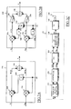
- FIG. 2A schematically shows, in terms of simplified functional blocks, an example of how the RF quadrature modulator 130 can be structured.
- the RF quadrature modulator 130 includes a pair of multipliers 210, 220, an adder 230 and a phase-shifter 240.
- the multiplier 220 receives the base-band signal Xq and the carrier wave C0 ; the multiplier 220 modulates the carrier wave C0 according to the base-band signal Xq , so as to generate a corresponding RF modulated signal RFXq ; in a similar way, the base-band signal Xi is provided to the multiplier 210 together with a phase-shifted version of the carrier wave C0 generated by the phase-shifter 240, in order to obtain a corresponding RF modulated signal RFXi . More particularly, the phase-shifter 240 is designed to introduce a phase-shift of 90 degrees on the carrier wave C0 , so that the RF modulated signals RFXq, RFXi are in quadrature to each other. The RF modulated signals RFXq, RFXi are then provided to the adder 230 for being summed to each other so as to obtain the RF modulated signal Y .
- phase imbalance is represented by two phase imbalance blocks 250 , 260.
- the phase imbalance block 250 acts on the input of the multiplier 220 receiving the carrier wave C0 by introducing a phase shift ⁇ , hereinafter referred to as phase error
- phase imbalance block 260 acts on the input of the multiplier 210 receiving the shifted carrier wave C0 by introducing a phase error - ⁇ .
- the gain imbalance is represented in FIG. 2B by means of two gain imbalance blocks 270 and 280 that act on the RF modulated signals RFXq and RFXi , respectively.
- the effect of the gain imbalance block 270 is a reduction of the amplitude of the RF modulated signal RFXq , which is amplified by an amount equal to (1- ⁇ ) - where the term ⁇ , hereinafter referred to as gain error, is a positive number lower than the unity;
- the effect of the gain imbalance block 280 is instead an increase of the amplitude of the RF modulated signal RFXi , which is amplified by an amount equal to (1+ ⁇ ).
- the RF modulated signals RFXi , RFXq experience an - undesired - gain difference equal to 2 ⁇ .
- Y bb Yi + jYq (wherein Yi , Yq are the real and imaginary parts thereof).
- ⁇ 1 and ⁇ 2 can be simplified in the following way: ⁇ 1 ⁇ 1 + j ⁇ ⁇ ⁇ ⁇ 2 ⁇ ⁇ + j ⁇
- phase and gain imbalances generates a signal component proportional to the complex conjugate of the equivalent base-band signal X .
- This signal component is capable of altering the base-band modulated signal Y bb to an extent such as to dull the performance of the whole telecommunication system.
- a compensator 290 is provided between the base-band signals generator 110 and the DAC circuit 120 .
- the compensator 290 modifies the signals received from the base-band signals generator 110 based on phase and gain compensation parameters ⁇ c , ⁇ c (with the modified signals that are denoted with the same references).
- the compensation parameters ⁇ c , ⁇ c are determined during a calibration phase that is performed before the transmitter TX is employed for its normal operation.
- FIG. 3 illustrates a calibration system 300 capable of estimating (during the calibration phase) the compensation parameters ⁇ c , ⁇ c .
- the calibration system 300 During the calibration phase, the calibration system 300 generates proper digitally modulated signals XDi , XDq that are provided to the DAC circuit 120 . As previously described, the DAC circuit 120 converts the signals into the corresponding base-band signals Xi , Xq that are provided to the RF quadrature modulator 130 . The resulting RF modulated signal Y (which, in general, is affected by the phase error ⁇ and gain error ⁇ ) is then feedback to the calibration system 300 . The calibration system 300 analyzes the RF modulated signal Y for establishing how the transmitter TX has to be calibrated for reducing the effects of the phase error ⁇ and gain error ⁇ , and accordingly generates the compensation parameters ⁇ c , ⁇ c .
- the calibration system 300 includes a test generator 310 for the generation of a pair of test signals XTi , XTq .
- the test generator 310 is included in the base-band signals generator, and it is deactivated during the normal operation of the transmitter TX ; alternatively, the test generator 310 is a dedicated apparatus that is available only during the calibration phase.
- the test signals XTi, XTq are provided to the compensator 290 , which is also configured to receive the phase compensation parameter ⁇ c and the gain compensation parameter ⁇ c .
- the compensator 290 modifies the received test signals XTi , XTq and accordingly generates the digitally modulated signals XDi , XDq to be provided to the DAC circuit 120 .
- the calibration phase for estimating the compensation parameters ⁇ c , ⁇ c provides for the iterative repetition of the same operations on different pairs of test signals XTi , XTq ; thus, for the sake of clarity, some of the quantities (e.g., signals and parameters) generated and/or exploited during a generic k-th iteration of the calibration phase will be specifically identified with an index " k ".
- a plurality of pairs of test signals in quadrature to each other are generated.
- Each pair of test signals is modulated to obtain a corresponding modulated signal.
- the modulated signals are squared, and then converted into the frequency domain.
- the modulus (or, according to an alternative embodiment of the present invention, the square of the modulus) of the transformed signals so obtained are then stored for being used to estimate the error to be corrected, in order to calculate a corresponding compensation.
- V k cos ( ⁇ k )+jsin( ⁇ k )
- ⁇ k k(2 ⁇ /N).
- the constant energy is distributed between the test signals XTik , XTqk of each pair in a different way.
- the calibration system 300 further includes a non-linear quadratic block 330, for example a Gilbert cell circuit, coupled to the output of the RF quadrature modulator 130 for receiving the RF modulated signal Yk .
- the squared modulated signal Rk is then provided to an ADC 340, which digitalizes the squared modulated signal Rk for providing a digitalized version thereof, referred to as digital squared signal DRk , to an estimator 350 .
- Fk bb ( Rk bb ,f ) at a frequency 2 f t (i.e., at a frequency that is twice the frequency f t of the test signals XTik , XTqk ):
- FIG. 4 shows a flow chart 400 illustrating the operations performed during the calibration phase.
- the calibration phase illustrated by the flow chart 400 provides for the cyclic iteration of an external loop.
- the flow of activity of the calibration phase initiates at block 401 , and then passes to block 403, wherein a counter j (defining the j-th iteration of the external loop) is set to zero.
- the flow of activity proceeds to block 405 , wherein the calibration system checks if the counter j has reached or not a threshold TH (such as 2-3), whose value depends on the desired accuracy of the calibration process.
- a threshold TH such as 2-3
- the flow of activity continues to block 407, wherein the index k (identifying the k-th pair of test signals XTik , XTqk ) is set to zero.
- the base-band modulated signal Yk is provided to the non-linear quadratic block, which calculates the squared modulated signal Rk .
- the squared modulated signal Rk is converted into the corresponding digital squared signal DRk, which is provided to the estimator.
- the partial error indicator Mk is then stored by the estimator at the block 419.
- the k-th iteration of the internal loop terminates at the block 421 , wherein the index k is incremented by one.
- the flow of activity proceeds to block 423 , wherein the calibration system checks if the index k has reached or not the value N -1. If not (exit branch " N "), the flow of activity returns back to block 409 , and a new iteration of the internal loop is performed, with a different pair of test signals XTik , XTqk .
- the flow of activity then continues to block 427 , wherein the estimator calculates the phase compensation parameter ⁇ c and the gain compensation parameter ⁇ c for compensating the phase error ⁇ and the gain error ⁇ that have been estimated.
- the values of the phase compensation parameter ⁇ c and of the gain compensation parameter ⁇ c are set to the opposite of the phase error ⁇ and of the gain error ⁇ , respectively, previously calculated.
- the flow of activity passes now to block 429 , wherein the phase compensation parameter ⁇ c and the gain compensation parameter ⁇ c are provided to the compensator; then, at block 431 , the index j is incremented by one (this means that the flow of activity is configured to initiate a further (j+1)-th iteration of the external loop).
- test signals XTik , XTqk generated at each k-th iteration of the internal loop are now compensated by the compensator with the phase compensation parameter ⁇ c and the gain compensation parameter ⁇ c calculated in the previous j-th iteration of the external loop.
- the repetition of the external loop is advantageously performed by the calibration system to guarantee an effective and precise compensation of the modulation errors: indeed, the process of calculating the partial error indicators Mk requires the use of some approximations, that may affect the compensation results. By repeating all these operations more than once (more particularly, a number of times equal to the threshold value TH ), it is assured that the negative effects of the approximations are diminished.
- the flow of activity proceeds to block 433 , wherein the compensation parameters ⁇ c , ⁇ c that have been calculated in the last iteration of the external loop are stored; these values may then be used in the transmitter during its normal operation for counterbalancing the negative effects of the errors on the modulation process.
- the method then ends at the final block 435 .
- the estimator should perform operations directed to the computation of a modulus (i.e., the modulus of the Fourier transform of the squared modulated signal Rk ). These operations are quite complex, since they include the calculation of a square root, and require a non-negligible amount of computing resources from the estimator.
- the proposed solution may be implemented with an equivalent method (using similar steps, removing non essential steps or adding optional steps).
- test signals of each pair have phase differences that are slightly different than 90 degrees; similar considerations apply in case the pairs of test signals have energies that are not equal, but instead differ by a small amount.
- modulation errors include different errors other than the phase and gain errors.
- the proposed solution may be applied to different transmitter apparatuses, in which the modulation is carried out in a different way.
- Transmitters including embodiments of the present invention may be contained in a variety of different types of electronic systems and devices, such as cellular telephones, personal digital assistants, computer systems, and so on.
Landscapes
- Engineering & Computer Science (AREA)
- Computer Networks & Wireless Communication (AREA)
- Signal Processing (AREA)
- Digital Transmission Methods That Use Modulated Carrier Waves (AREA)
Applications Claiming Priority (1)
| Application Number | Priority Date | Filing Date | Title |
|---|---|---|---|
| US12/040,712 US7953379B2 (en) | 2008-02-29 | 2008-02-29 | Method and system for calibrating quadrature modulators |
Publications (1)
| Publication Number | Publication Date |
|---|---|
| EP2096818A2 true EP2096818A2 (fr) | 2009-09-02 |
Family
ID=40765546
Family Applications (1)
| Application Number | Title | Priority Date | Filing Date |
|---|---|---|---|
| EP09153929A Withdrawn EP2096818A2 (fr) | 2008-02-29 | 2009-02-27 | Procédé et système pour étalonner des modulateurs de quadrature |
Country Status (2)
| Country | Link |
|---|---|
| US (1) | US7953379B2 (fr) |
| EP (1) | EP2096818A2 (fr) |
Families Citing this family (6)
| Publication number | Priority date | Publication date | Assignee | Title |
|---|---|---|---|---|
| TWI358910B (en) * | 2008-03-25 | 2012-02-21 | Mstar Semiconductor Inc | Circuit and method of calibrating direct current o |
| US8224268B2 (en) * | 2009-01-21 | 2012-07-17 | Texas Instruments Incorporated | Transmitter linearization |
| US8406283B2 (en) * | 2009-07-20 | 2013-03-26 | Advantest Corporation | Modulation apparatus, test apparatus and correction method |
| JP5290098B2 (ja) * | 2009-09-10 | 2013-09-18 | ルネサスエレクトロニクス株式会社 | 送信機およびそれに使用可能な半導体集積回路 |
| US20120294343A1 (en) * | 2011-05-16 | 2012-11-22 | Phase Matrix, Inc. | RF I/Q Modulator with Sampling Calibration System |
| CN117395707B (zh) * | 2023-12-11 | 2024-03-19 | 深圳市天龙世纪科技发展有限公司 | 一种mtk耦合测试方法、系统及介质 |
Family Cites Families (9)
| Publication number | Priority date | Publication date | Assignee | Title |
|---|---|---|---|---|
| US6058291A (en) * | 1997-12-03 | 2000-05-02 | 3Com Corporation | Methods and apparatus for carrier suppression in a radio modulator |
| US6265949B1 (en) * | 1999-12-22 | 2001-07-24 | Lg Information & Communications, Ltd. | Phase compensation apparatus and method for a digital modulator |
| US6421397B1 (en) * | 2000-01-28 | 2002-07-16 | Alcatel Canada Inc. | Modulation system having on-line IQ calibration |
| US6421398B1 (en) * | 2000-01-28 | 2002-07-16 | Alcatel Canada Inc. | Modulation system having on-line IQ calibration |
| US6704551B2 (en) * | 2001-02-21 | 2004-03-09 | Koninklijke Philips Electronics N.V. | Calibration of in-phase and quadrature transmit branches of a transmitter |
| US6771709B2 (en) * | 2001-10-16 | 2004-08-03 | Her Majesty The Queen In Right Of Canada, As Represented By The Minister Of Industry | System and method for direct transmitter self-calibration |
| DE602004025561D1 (de) * | 2003-04-24 | 2010-04-01 | Nxp Bv | Quadraturmodulator und kalibrierungsverfahren dafür |
| US7734261B2 (en) * | 2004-12-16 | 2010-06-08 | Nxp B.V. | Calibrating amplitude and phase imbalance and DC offset of an analog I/Q modulator in a high-frequency transmitter |
| US7925228B2 (en) * | 2008-02-29 | 2011-04-12 | Stmicroelectronics, S.R.L. | Method and system for calibrating quadrature modulators |
-
2008
- 2008-02-29 US US12/040,712 patent/US7953379B2/en active Active
-
2009
- 2009-02-27 EP EP09153929A patent/EP2096818A2/fr not_active Withdrawn
Non-Patent Citations (1)
| Title |
|---|
| J. K. CAVERS: "New Methods for Adaptation of Quadrature Modulators and Demodulators in Amplifier Linearization Circuits", TRANSACTION ON VEHICULAR TECHNOLOGY, vol. 46, 3 August 1997 (1997-08-03) |
Also Published As
| Publication number | Publication date |
|---|---|
| US20090221247A1 (en) | 2009-09-03 |
| US7953379B2 (en) | 2011-05-31 |
Similar Documents
| Publication | Publication Date | Title |
|---|---|---|
| US6771709B2 (en) | System and method for direct transmitter self-calibration | |
| US20160359614A1 (en) | Adaptive I/Q Mismatch Calibration | |
| KR101234963B1 (ko) | Ofdm fdd 통신 시스템에서의 송신 및 수신 경로들의 i/q 교정 | |
| US6842489B2 (en) | Coherent adaptive calibration system and method | |
| US9537520B2 (en) | Method and apparatus for calibrating distortion of signals | |
| CN100481828C (zh) | 正交调制器幅度失衡补偿 | |
| US20100297966A1 (en) | Measuring and Correcting Errors in a Transmit Chain with an IQ Up-Converter and IQ Down-Converter | |
| EP2096818A2 (fr) | Procédé et système pour étalonner des modulateurs de quadrature | |
| US20120270516A1 (en) | Receiver for estimating and compensating for in-phase/quadrature mismatch | |
| US7933348B2 (en) | DC offset estimation system and method | |
| US20120250790A1 (en) | Frequency selective iq correction | |
| US8526533B2 (en) | Systems and methods for measuring I-Q mismatch | |
| US8644424B2 (en) | Receiver apparatus, communication system, reception method and communication method | |
| JP4211019B2 (ja) | 無線装置及びその送信波の歪補償方法 | |
| CN1835489B (zh) | 一种可补偿同相/正交相不平衡的装置及其方法 | |
| US7925228B2 (en) | Method and system for calibrating quadrature modulators | |
| KR100960022B1 (ko) | 디지털 중간주파수 무선송신기, 고주파 변조 장치 및 방법 | |
| US9106326B2 (en) | Method for determining the imperfections of a transmit pathway and of a receive pathway of an apparatus, and associated radio apparatus | |
| US7450919B1 (en) | I/Q mismatch correction using transmitter leakage and gain modulation | |
| US20250088404A1 (en) | Electronic device and operating method to compensate for in-phase/quadrature imbalance | |
| KR20010076760A (ko) | 배열 송수신부의 오차 보정장치 및 방법 | |
| US20070159162A1 (en) | Method and apparatus for self-calibration in a mobile transceiver | |
| US7164327B2 (en) | Compensation of the IQ phase asymmetry in quadrature modulation and demodulation methods | |
| Shimoda et al. | Demonstration of Measurement Method based on Under-sampling for mmWave Radio Communication Signals | |
| US20180083823A1 (en) | Transmission and reception circuit, transceiver, and method of correcting time difference of signal |
Legal Events
| Date | Code | Title | Description |
|---|---|---|---|
| PUAI | Public reference made under article 153(3) epc to a published international application that has entered the european phase |
Free format text: ORIGINAL CODE: 0009012 |
|
| AK | Designated contracting states |
Kind code of ref document: A2 Designated state(s): AT BE BG CH CY CZ DE DK EE ES FI FR GB GR HR HU IE IS IT LI LT LU LV MC MK MT NL NO PL PT RO SE SI SK TR |
|
| AX | Request for extension of the european patent |
Extension state: AL BA RS |
|
| RAP1 | Party data changed (applicant data changed or rights of an application transferred) |
Owner name: STMICROELECTRONICS SRL |
|
| RAP1 | Party data changed (applicant data changed or rights of an application transferred) |
Owner name: STMICROELECTRONICS SRL |
|
| STAA | Information on the status of an ep patent application or granted ep patent |
Free format text: STATUS: THE APPLICATION IS DEEMED TO BE WITHDRAWN |
|
| 18D | Application deemed to be withdrawn |
Effective date: 20120901 |