EP2096905A1 - Verfahren zum Aufbauen von elektronischen und/oder elektrooptischen Vorrichtungen auf einer Elektroleiterplatte - Google Patents
Verfahren zum Aufbauen von elektronischen und/oder elektrooptischen Vorrichtungen auf einer Elektroleiterplatte Download PDFInfo
- Publication number
- EP2096905A1 EP2096905A1 EP08425114A EP08425114A EP2096905A1 EP 2096905 A1 EP2096905 A1 EP 2096905A1 EP 08425114 A EP08425114 A EP 08425114A EP 08425114 A EP08425114 A EP 08425114A EP 2096905 A1 EP2096905 A1 EP 2096905A1
- Authority
- EP
- European Patent Office
- Prior art keywords
- electronic
- electro
- optical devices
- solder material
- board
- Prior art date
- Legal status (The legal status is an assumption and is not a legal conclusion. Google has not performed a legal analysis and makes no representation as to the accuracy of the status listed.)
- Withdrawn
Links
Images
Classifications
-
- H—ELECTRICITY
- H05—ELECTRIC TECHNIQUES NOT OTHERWISE PROVIDED FOR
- H05K—PRINTED CIRCUITS; CASINGS OR CONSTRUCTIONAL DETAILS OF ELECTRIC APPARATUS; MANUFACTURE OF ASSEMBLAGES OF ELECTRICAL COMPONENTS
- H05K3/00—Apparatus or processes for manufacturing printed circuits
- H05K3/30—Assembling printed circuits with electric components, e.g. with resistors
- H05K3/32—Assembling printed circuits with electric components, e.g. with resistors electrically connecting electric components or wires to printed circuits
- H05K3/34—Assembling printed circuits with electric components, e.g. with resistors electrically connecting electric components or wires to printed circuits by soldering
- H05K3/346—Solder materials or compositions specially adapted therefor
-
- B—PERFORMING OPERATIONS; TRANSPORTING
- B23—MACHINE TOOLS; METAL-WORKING NOT OTHERWISE PROVIDED FOR
- B23K—SOLDERING OR UNSOLDERING; WELDING; CLADDING OR PLATING BY SOLDERING OR WELDING; CUTTING BY APPLYING HEAT LOCALLY, e.g. FLAME CUTTING; WORKING BY LASER BEAM
- B23K35/00—Rods, electrodes, materials, or media, for use in soldering, welding, or cutting
- B23K35/22—Rods, electrodes, materials, or media, for use in soldering, welding, or cutting characterised by the composition or nature of the material
- B23K35/24—Selection of soldering or welding materials proper
- B23K35/26—Selection of soldering or welding materials proper with the principal constituent melting at less than 400°C
- B23K35/262—Sn as the principal constituent
-
- B—PERFORMING OPERATIONS; TRANSPORTING
- B23—MACHINE TOOLS; METAL-WORKING NOT OTHERWISE PROVIDED FOR
- B23K—SOLDERING OR UNSOLDERING; WELDING; CLADDING OR PLATING BY SOLDERING OR WELDING; CUTTING BY APPLYING HEAT LOCALLY, e.g. FLAME CUTTING; WORKING BY LASER BEAM
- B23K35/00—Rods, electrodes, materials, or media, for use in soldering, welding, or cutting
- B23K35/22—Rods, electrodes, materials, or media, for use in soldering, welding, or cutting characterised by the composition or nature of the material
- B23K35/24—Selection of soldering or welding materials proper
- B23K35/26—Selection of soldering or welding materials proper with the principal constituent melting at less than 400°C
- B23K35/264—Bi as the principal constituent
-
- H—ELECTRICITY
- H05—ELECTRIC TECHNIQUES NOT OTHERWISE PROVIDED FOR
- H05K—PRINTED CIRCUITS; CASINGS OR CONSTRUCTIONAL DETAILS OF ELECTRIC APPARATUS; MANUFACTURE OF ASSEMBLAGES OF ELECTRICAL COMPONENTS
- H05K1/00—Printed circuits
- H05K1/02—Details
- H05K1/0201—Thermal arrangements, e.g. for cooling, heating or preventing overheating
- H05K1/0203—Cooling of mounted components
-
- H—ELECTRICITY
- H05—ELECTRIC TECHNIQUES NOT OTHERWISE PROVIDED FOR
- H05K—PRINTED CIRCUITS; CASINGS OR CONSTRUCTIONAL DETAILS OF ELECTRIC APPARATUS; MANUFACTURE OF ASSEMBLAGES OF ELECTRICAL COMPONENTS
- H05K2201/00—Indexing scheme relating to printed circuits covered by H05K1/00
- H05K2201/10—Details of components or other objects attached to or integrated in a printed circuit board
- H05K2201/10007—Types of components
- H05K2201/10106—Light emitting diode [LED]
-
- H—ELECTRICITY
- H05—ELECTRIC TECHNIQUES NOT OTHERWISE PROVIDED FOR
- H05K—PRINTED CIRCUITS; CASINGS OR CONSTRUCTIONAL DETAILS OF ELECTRIC APPARATUS; MANUFACTURE OF ASSEMBLAGES OF ELECTRICAL COMPONENTS
- H05K2201/00—Indexing scheme relating to printed circuits covered by H05K1/00
- H05K2201/10—Details of components or other objects attached to or integrated in a printed circuit board
- H05K2201/10613—Details of electrical connections of non-printed components, e.g. special leads
- H05K2201/10954—Other details of electrical connections
- H05K2201/10969—Metallic case or integral heatsink of component electrically connected to a pad on PCB
-
- H—ELECTRICITY
- H05—ELECTRIC TECHNIQUES NOT OTHERWISE PROVIDED FOR
- H05K—PRINTED CIRCUITS; CASINGS OR CONSTRUCTIONAL DETAILS OF ELECTRIC APPARATUS; MANUFACTURE OF ASSEMBLAGES OF ELECTRICAL COMPONENTS
- H05K3/00—Apparatus or processes for manufacturing printed circuits
- H05K3/30—Assembling printed circuits with electric components, e.g. with resistors
- H05K3/32—Assembling printed circuits with electric components, e.g. with resistors electrically connecting electric components or wires to printed circuits
- H05K3/34—Assembling printed circuits with electric components, e.g. with resistors electrically connecting electric components or wires to printed circuits by soldering
- H05K3/341—Surface mounted components
Definitions
- the present invention relates to a process for mounting electronic and/or electro-optical devices on an electronic board.
- LED's Light-Emitting Diodes
- the first step aims at laying a material that when manufacture of the item has been completed, will allow an electric connection between the device and the remainder of the circuit on the board, while the second step aims at enabling a suitable heat dissipation for the device.
- laying of the adhesive material at the so-called central "bump contact" of the LED in addition to optimising heat dissipation, also allows a mechanical constraint to be obtained between the LED and the board on which the device is mounted.
- a first drawback in this type of processes resides in that the double laying step (first the soldering cream and then the adhesive material) makes the time for carrying out the process very long, which will involve a limitation in the production efficiency.
- a further drawback is the high cost, due to the expendable materials and the need for suitable apparatus adapted to perform the two distinct steps.
- Solders presently used e.g. tin-lead alloys, lead-free alloys (SAC), etc.
- SAC lead-free alloys
- the present invention aims at providing a process for mounting electronic and/or electro-optical devices on electronic boards that is quick and of easy execution.
- Another aim of the invention is to make available a process enabling a reliable connection to be obtained, both from an electric and a mechanical point of view, between the device and the board on which the latter is mounted.
- a further aim of the invention is to make available a process that does not impair the qualities, features and good operation of the devices that are mounted on the board.
- a still further aim of the invention is to provide a process allowing a reduction to be achieved in the overall costs for mounting of said electronic and/or electro-optical devices.
- Another aim of the invention is to make available a process by which also different types of electronic and/or electro-optical devices can be mounted in a quick and reliable manner.
- the process of the invention applies to the field of surface mount of electronic, opto-electronic, electro-optical, etc. devices (SMD) on electronic boards.
- SMD surface mount of electronic, opto-electronic, electro-optical, etc. devices
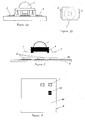
- the inventive process first of all comprises a step of providing an electronic board 6 (diagrammatically shown in Figs. 2 and 3 ).
- the electronic board 6 has a printed circuit on a surface 6a thereof, which circuit is designed to be associated with one or more electronic and/or electro-optical devices.
- the electronic board 6 can be formed with FR4 (Flame Retardant 4) or with an aluminium or copper substrate (MC-PCB).
- FR4 Flume Retardant 4
- MC-PCB aluminium or copper substrate
- the process according to the invention further comprises a step of laying a solder material comprising a tin-bismuth solder or alloy 5 on the electronic board 6 and in particular on surface 6a.
- the tin-bismuth solder 5 comprises a percentage of 30% to 50%, and in particular of 40% to 45%, of tin by weight; by way of example, the percent by weight of tin can be of about 43%.
- the tin-bismuth solder 5 comprises a percent by weight of bismuth included between 50% and 70% and in particular between 55% and 60%; by way of example, the percent by weight of tin can be of about 57%.
- the melting temperature of alloy 5 is included between 130°C and 150°C, and in particular between 135°C and 140°C; by way of example, this melting temperature can be of about 138°C.
- an alloy having the standard code J-STD-006 can be employed, the features of said alloy being summarised in the following table: Alloy for solder paste: Tin-Bismuth Composition (% by weight): Tin: 43% - Bismuth: 57% Metal content: 87-88% Particle size: 38-53 ⁇ , Melting point: 138°C Standard reference: J-STD-006
- the process according to the invention further comprises a step of positioning said one or more electronic and/or electro-optical devices on the electronic board 6, and in particular on one or more respective areas on which the solder material 5 has been laid.
- said one or more electronic and/or electro-optical devices comprise at least one LED 1.
- LED 1 has a predetermined number of electric contacts (two electric contacts, for example), 2, 3 and a dissipation region 4.
- solder material 5 is interposed between the electronic board 6 and LED 1 so that said material is positioned both at the electric contacts 2, 3 and at the dissipation region 4.
- solder material 5 is used both for an electric connection between LED 1 and the electronic board 6, and for a mechanical constraint between the same elements to enable a suitable dissipation of the heat produced by said LED 1.
- the solder material 5 is laid on the electronic board 6 by a single laying step, since the solder material 5 is able to obtain all necessary effects for an efficient mounting of LED 1 (i.e. electric connection and heat dissipation).
- solder material 5 is sufficient to perform the different necessary functions.
- the semi-finished product thus obtained is heated following a predetermined thermal profile, to enable the solder material to melt and perform its fastening action.
- This heating step can be performed by means of a reflow oven or a hot plate, for example.
- the semifinished product is allowed to cool (until it reaches a temperature close to the room temperature, for example), so that the solder material 5 can solidify and complete the assembling process.
- said electronic devices also comprise at least one device that is not a LED, denoted at 1a in Fig. 3 , by way of example.
- device 1a can be a resistor, a transistor, a capacitor, an inductor, etc., generally any device that can be soldered to the electronic board 6 following an SMD technology.
- the invention achieves important advantages.
- the process according to the invention can be carried out in a quick and simple manner.
- accomplishment of the process can take place by means of apparatus and instruments of reduced complexity.
- a further advantage consists in that the inventive process allows a reliable both electric and mechanical connection to be obtained between the device and the board on which the latter is mounted.
- Another advantage is found in that the mounting process does not impair the qualities, features and good operation of the devices mounted on said board.
- a still further advantage resides in that the process of the invention can be efficiently used for mounting also different typologies of electronic and/or electro-optical devices in a quick and reliable manner.
Landscapes
- Engineering & Computer Science (AREA)
- Mechanical Engineering (AREA)
- Manufacturing & Machinery (AREA)
- Microelectronics & Electronic Packaging (AREA)
- Electric Connection Of Electric Components To Printed Circuits (AREA)
Priority Applications (1)
| Application Number | Priority Date | Filing Date | Title |
|---|---|---|---|
| EP08425114A EP2096905A1 (de) | 2008-02-26 | 2008-02-26 | Verfahren zum Aufbauen von elektronischen und/oder elektrooptischen Vorrichtungen auf einer Elektroleiterplatte |
Applications Claiming Priority (1)
| Application Number | Priority Date | Filing Date | Title |
|---|---|---|---|
| EP08425114A EP2096905A1 (de) | 2008-02-26 | 2008-02-26 | Verfahren zum Aufbauen von elektronischen und/oder elektrooptischen Vorrichtungen auf einer Elektroleiterplatte |
Publications (1)
| Publication Number | Publication Date |
|---|---|
| EP2096905A1 true EP2096905A1 (de) | 2009-09-02 |
Family
ID=39665941
Family Applications (1)
| Application Number | Title | Priority Date | Filing Date |
|---|---|---|---|
| EP08425114A Withdrawn EP2096905A1 (de) | 2008-02-26 | 2008-02-26 | Verfahren zum Aufbauen von elektronischen und/oder elektrooptischen Vorrichtungen auf einer Elektroleiterplatte |
Country Status (1)
| Country | Link |
|---|---|
| EP (1) | EP2096905A1 (de) |
Cited By (1)
| Publication number | Priority date | Publication date | Assignee | Title |
|---|---|---|---|---|
| WO2019226438A1 (en) * | 2018-05-20 | 2019-11-28 | Abeyatech, Llc | Light emitting diode for low temperature applications |
Citations (6)
| Publication number | Priority date | Publication date | Assignee | Title |
|---|---|---|---|---|
| US5368814A (en) * | 1993-06-16 | 1994-11-29 | International Business Machines, Inc. | Lead free, tin-bismuth solder alloys |
| WO1994027777A1 (en) * | 1993-06-01 | 1994-12-08 | Motorola Inc. | Tin-bismuth solder paste and method of use |
| EP0711629A1 (de) * | 1994-11-08 | 1996-05-15 | AT&T Corp. | Bleifreies niedrigschmelzendes Lot mit verbesserten mechanischen Eigenschaften und mit diesem Lot verbundene Gegenstände |
| US20010002982A1 (en) * | 1996-06-12 | 2001-06-07 | Sarkhel Amit Kumar | Lead-free, high tin ternary solder alloy of tin, silver, and bismuth |
| DE10234995A1 (de) * | 2002-07-31 | 2004-02-12 | Osram Opto Semiconductors Gmbh | Leuchtdiodenanordnung mit thermischem Chipanschluß und Leuchtdiodenmodul |
| US6820798B1 (en) * | 1999-03-04 | 2004-11-23 | Conti Temic Microelectronic Gmbh | Method for producing circuit arrangments |
-
2008
- 2008-02-26 EP EP08425114A patent/EP2096905A1/de not_active Withdrawn
Patent Citations (6)
| Publication number | Priority date | Publication date | Assignee | Title |
|---|---|---|---|---|
| WO1994027777A1 (en) * | 1993-06-01 | 1994-12-08 | Motorola Inc. | Tin-bismuth solder paste and method of use |
| US5368814A (en) * | 1993-06-16 | 1994-11-29 | International Business Machines, Inc. | Lead free, tin-bismuth solder alloys |
| EP0711629A1 (de) * | 1994-11-08 | 1996-05-15 | AT&T Corp. | Bleifreies niedrigschmelzendes Lot mit verbesserten mechanischen Eigenschaften und mit diesem Lot verbundene Gegenstände |
| US20010002982A1 (en) * | 1996-06-12 | 2001-06-07 | Sarkhel Amit Kumar | Lead-free, high tin ternary solder alloy of tin, silver, and bismuth |
| US6820798B1 (en) * | 1999-03-04 | 2004-11-23 | Conti Temic Microelectronic Gmbh | Method for producing circuit arrangments |
| DE10234995A1 (de) * | 2002-07-31 | 2004-02-12 | Osram Opto Semiconductors Gmbh | Leuchtdiodenanordnung mit thermischem Chipanschluß und Leuchtdiodenmodul |
Non-Patent Citations (1)
| Title |
|---|
| PHILLIPS J ET AL: "EUTECTIC TIN-BISMUTH FOR TWO-STEP PCB SOLDERING", ELECTRONIC PACKAGING AND PRODUCTION, CAHNERS PUBLISHING CO, NEWTON, MASSACHUSETTS, US, vol. 32, no. 2, 1 February 1992 (1992-02-01), pages 78 - 80, XP000259200, ISSN: 0013-4945 * |
Cited By (3)
| Publication number | Priority date | Publication date | Assignee | Title |
|---|---|---|---|---|
| WO2019226438A1 (en) * | 2018-05-20 | 2019-11-28 | Abeyatech, Llc | Light emitting diode for low temperature applications |
| EA039238B1 (ru) * | 2018-05-20 | 2021-12-21 | Абеятек, Ллс | Светоизлучающий диод для применения при низких температурах |
| US12159961B2 (en) | 2018-05-20 | 2024-12-03 | Azenta Life Sciences, Inc. | Light emitting diode for low temperature applications |
Similar Documents
| Publication | Publication Date | Title |
|---|---|---|
| JP4144415B2 (ja) | 鉛フリーはんだ | |
| KR102087004B1 (ko) | 솔더 프리폼과 솔더 합금 조립 방법 | |
| US8059424B2 (en) | Electronic board incorporating a heating resistor | |
| US20090050677A1 (en) | Method of welding electronic components on pcbs | |
| BR112012015939A8 (pt) | método para soldar componente de montagem em superfície e componente de montagem em superfície | |
| JP2004141910A (ja) | 鉛フリーはんだ合金 | |
| US20090126980A1 (en) | Printed wiring board | |
| CN114682870B (zh) | 一种pop元件堆叠装配的混合焊接工艺及系统 | |
| US6168070B1 (en) | Method for soldering DPAK-type electronic components to circuit boards | |
| US9254531B2 (en) | PCB mounting method | |
| EP2096905A1 (de) | Verfahren zum Aufbauen von elektronischen und/oder elektrooptischen Vorrichtungen auf einer Elektroleiterplatte | |
| EP1294217A1 (de) | Verfahren zur montage eines elektronischen bauteils | |
| US7743491B2 (en) | Mounting method of passive component | |
| US20190013308A1 (en) | Die bonding to a board | |
| JP2015205293A (ja) | はんだペースト、電子装置の製造方法および電子装置 | |
| JP2007243118A (ja) | 半導体装置 | |
| Holtzer et al. | Eliminating wave soldering with low melting point solder paste | |
| JP2003060336A (ja) | 半導体装置及び半導体パッケージの実装方法 | |
| KR100540044B1 (ko) | 표면실장부품 리워크용 납 조성물 | |
| US20130301231A1 (en) | Method for producing an electronic module by means of sequential fixation of the components, and corresponding production line | |
| JP2002158438A (ja) | 電子制御装置 | |
| EP3364733A1 (de) | Verfahren zum erhalten von thermischem gleichgewicht bei der herstellung von leiterplattenanordnungen | |
| Yuming et al. | Research on factors influencing the board level product quality | |
| Lau et al. | Lead-Free Wave-Soldering and Reliability of Light-Emitting Diode (LED) Display Assemblies | |
| KR101296372B1 (ko) | 프리 리플로우 방식의 이종재질 솔더간 솔더링 장치 및 솔더링 방법 |
Legal Events
| Date | Code | Title | Description |
|---|---|---|---|
| PUAI | Public reference made under article 153(3) epc to a published international application that has entered the european phase |
Free format text: ORIGINAL CODE: 0009012 |
|
| AK | Designated contracting states |
Kind code of ref document: A1 Designated state(s): AT BE BG CH CY CZ DE DK EE ES FI FR GB GR HR HU IE IS IT LI LT LU LV MC MT NL NO PL PT RO SE SI SK TR |
|
| AX | Request for extension of the european patent |
Extension state: AL BA MK RS |
|
| AKX | Designation fees paid | ||
| REG | Reference to a national code |
Ref country code: DE Ref legal event code: 8566 |
|
| STAA | Information on the status of an ep patent application or granted ep patent |
Free format text: STATUS: THE APPLICATION IS DEEMED TO BE WITHDRAWN |
|
| 18D | Application deemed to be withdrawn |
Effective date: 20100303 |