EP2097935B1 - Lichtemissionsvorrichtung mit geformtem wellenlängenumrichter - Google Patents
Lichtemissionsvorrichtung mit geformtem wellenlängenumrichter Download PDFInfo
- Publication number
- EP2097935B1 EP2097935B1 EP07849489.5A EP07849489A EP2097935B1 EP 2097935 B1 EP2097935 B1 EP 2097935B1 EP 07849489 A EP07849489 A EP 07849489A EP 2097935 B1 EP2097935 B1 EP 2097935B1
- Authority
- EP
- European Patent Office
- Prior art keywords
- light
- ceramic body
- ceramic
- top surface
- emitting apparatus
- Prior art date
- Legal status (The legal status is an assumption and is not a legal conclusion. Google has not performed a legal analysis and makes no representation as to the accuracy of the status listed.)
- Active
Links
Images


Classifications
-
- H—ELECTRICITY
- H10—SEMICONDUCTOR DEVICES; ELECTRIC SOLID-STATE DEVICES NOT OTHERWISE PROVIDED FOR
- H10H—INORGANIC LIGHT-EMITTING SEMICONDUCTOR DEVICES HAVING POTENTIAL BARRIERS
- H10H20/00—Individual inorganic light-emitting semiconductor devices having potential barriers, e.g. light-emitting diodes [LED]
- H10H20/80—Constructional details
- H10H20/85—Packages
- H10H20/851—Wavelength conversion means
- H10H20/8514—Wavelength conversion means characterised by their shape, e.g. plate or foil
-
- G—PHYSICS
- G02—OPTICS
- G02B—OPTICAL ELEMENTS, SYSTEMS OR APPARATUS
- G02B19/00—Condensers, e.g. light collectors or similar non-imaging optics
- G02B19/0004—Condensers, e.g. light collectors or similar non-imaging optics characterised by the optical means employed
- G02B19/0028—Condensers, e.g. light collectors or similar non-imaging optics characterised by the optical means employed refractive and reflective surfaces, e.g. non-imaging catadioptric systems
-
- G—PHYSICS
- G02—OPTICS
- G02B—OPTICAL ELEMENTS, SYSTEMS OR APPARATUS
- G02B19/00—Condensers, e.g. light collectors or similar non-imaging optics
- G02B19/0033—Condensers, e.g. light collectors or similar non-imaging optics characterised by the use
- G02B19/0047—Condensers, e.g. light collectors or similar non-imaging optics characterised by the use for use with a light source
- G02B19/0061—Condensers, e.g. light collectors or similar non-imaging optics characterised by the use for use with a light source the light source comprising a LED
-
- H—ELECTRICITY
- H10—SEMICONDUCTOR DEVICES; ELECTRIC SOLID-STATE DEVICES NOT OTHERWISE PROVIDED FOR
- H10H—INORGANIC LIGHT-EMITTING SEMICONDUCTOR DEVICES HAVING POTENTIAL BARRIERS
- H10H20/00—Individual inorganic light-emitting semiconductor devices having potential barriers, e.g. light-emitting diodes [LED]
- H10H20/80—Constructional details
- H10H20/85—Packages
- H10H20/855—Optical field-shaping means, e.g. lenses
-
- G—PHYSICS
- G02—OPTICS
- G02B—OPTICAL ELEMENTS, SYSTEMS OR APPARATUS
- G02B2207/00—Coding scheme for general features or characteristics of optical elements and systems of subclass G02B, but not including elements and systems which would be classified in G02B6/00 and subgroups
- G02B2207/113—Fluorescence
-
- H—ELECTRICITY
- H10—SEMICONDUCTOR DEVICES; ELECTRIC SOLID-STATE DEVICES NOT OTHERWISE PROVIDED FOR
- H10H—INORGANIC LIGHT-EMITTING SEMICONDUCTOR DEVICES HAVING POTENTIAL BARRIERS
- H10H20/00—Individual inorganic light-emitting semiconductor devices having potential barriers, e.g. light-emitting diodes [LED]
- H10H20/80—Constructional details
- H10H20/85—Packages
- H10H20/855—Optical field-shaping means, e.g. lenses
- H10H20/856—Reflecting means
Definitions
- the invention relates to a light-emitting apparatus comprising a semiconductor light-emitting device and a ceramic wavelength conversion body.
- Such light-emitting apparatuses are well known and used in particular as light sources in indicators, display backlighting units, automotive (head-)lamps and general-purpose illuminators.
- a light-emitting apparatus of the kind set forth is known from US2005/0269582 . That document discloses a semiconductor device comprising a light-emitting layer disposed between an n-type and a p-type region in combination with a ceramic body, which is disposed in a path of the light emitted by the light-emitting layer.
- the ceramic body is composed of (or includes) a wavelength converting material, such as a phosphor.
- these ceramic materials are based on Yttrium Aluminum Garnet (YAG), Yttrium Aluminum Silicon Oxo-Nitrides (YSN), Silicon Aluminum Oxo-Nitrides (SiAlON) or Lutetium Aluminum Garnet (LuAG).
- the 'primary' light emitted by III-nitride LEDs can be converted into 'secondary' light having a longer peak wavelength than the primary light by using the above described ceramic materials.
- the wavelength converting material can be chosen to obtain a particular peak wavelength of the secondary light.
- the size and thickness of the ceramic body and / or the concentration of the wavelength converting material can be chosen such that the light emitted by the apparatus is either a mixture of 'primary' and 'secondary' light or substantially consists of only the 'secondary' light.
- the advantage of this approach lies in the fact that the above-described luminescent ceramic bodies are robust and show a low sensitivity to temperature changes. Furthermore, such luminescent ceramics exhibit (almost) no scattering and therefore have a good conversion efficiency compared to phosphor layers.
- the transparent luminescent ceramic body described in US2005/0269582 is a volume emitter with an index of refraction (substantially) larger than 1.
- US2005/0151141 describes a luminescence diode chip with a semiconductor body having an epitaxially grown semiconductor layer sequence with an active zone emitting an electromagnetic radiation during operation of the luminescence diode chip, which electromagnetic radiation, at least in part, is coupled out via the radiation coupling-out area.
- the luminescence diode chip has a radiation transmissive covering body that is arranged downstream of the radiation coupling-out area in an emission direction of the luminescence diode chip and has a first main surface facing the radiation coupling out-area, and also side faces connecting the first and second main areas.
- US2004/0145308 describes a light source having at least one LED for emitting a primary radiation and at least one luminescence conversion body having at least one luminescent material for converting the primary radiation into a secondary radiation.
- the luminescence conversion body is a polycrystalline ceramic body.
- the LED is based on GaInN and emits blue primary radiation.
- the ceramic body comprises for example a luminescent material based on a cerium-doped yttrium aluminum garnet. This luminescent material emits yellow secondary radiation. Blue primary radiation and yellow secondary radiation penetrate through the luminescence conversion body and are perceived as white light by the observer.
- the document further describes that for a high light power, it is particularly advantageous if the ceramic body is translucent and/or transparent to the primary radiation and/or to the secondary radiation.
- a light-emitting apparatus comprising a semiconductor light emitting device comprising a light-emitting layer disposed between an n-type region and a p-type region, a transparent ceramic body comprising a wavelength converting material positioned in light receiving relationship to the semiconductor device, the ceramic body further having a bottom surface facing towards the semiconductor device, wherein the ceramic body has at least one side surface at an oblique angle with respect to said bottom surface in order to unlock waveguide modes from said ceramic body as further defined in claim 1.
- the invention provides a light-emitting apparatus in which the wave-guide modes are unlocked through the application of the oblique side surfaces.
- the ceramic body can emit the light formerly trapped in these modes. Consequently the light output from the ceramic body can be more than twice as high as the light output from bodies without oblique side surfaces.
- the brightness of the device can be enhanced with about the same factor.
- the oblique angle is larger than 95° or smaller than 85°. Even better still, the oblique angle is larger than 100° or smaller than 80°.
- At least one oblique side surface of the ceramic body has a reflective coating. This is advantageous to enhance the flux through and the brightness of the top surface even further.
- an intermediate layer having a lower index of refraction than the ceramic body is accommodated between the body and the reflective coating.
- the efficiency of the reflection is improved by the application of the intermediate layer.
- the ceramic body has a top surface provided with a micro-corrugation.
- the application of a micro-corrugation enhances the light extraction from and/or the brightness of on the top surface of the ceramic body.
- the ceramic body has a top surface provided to include an optical function.
- an application specific radiation distribution from the light-emitting apparatus is realized.
- the ceramic body has a top surface provided with a reflective coating.
- This embodiment can beneficially used as a side emitter in certain application, e.g. to couple light into a light-guide.
- an intermediate layer having a lower index of refraction than the ceramic body is accommodated between the body and the reflective coating on the top surface.
- an intermediate layer having a lower index of refraction than the ceramic body is accommodated between the bottom surface and the semiconductor light-emitting device. Again this is beneficial to enhance the efficiency of the reflection at the bottom surface.
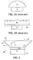
- Figs. 1A and 1B show two examples of a light-emitting apparatus comprising a semiconductor light-emitting device 52 and a ceramic wavelength conversion body 54, 50a, 50b as known from US2005/0269582 .
- the ceramic wavelength converting body 54 is shaped to form a dome lens.
- a second ceramic wavelength converting body 50b is shaped to form a Fresnel lens and located on top of a first rectangular ceramic wavelength converting body 50a.
- the lens shape of the body 54, 50b in the prior art should avoid total internal reflection (TIR) at the interface between the high index of refraction body and the low index of refraction air.
- TIR total internal reflection
- the TIR is avoided (or at least minimized) by shaping the lens 54 with a radius of curvature considerably larger than the light-emitting device 52. It is clear, however, that in both embodiments of Fig.1 TIR still occurs - and consequently locking of light in wave guide modes - even at the shaped surfaces of the ceramic wavelength conversion bodies 50a, 50b, 54. Furthermore, due to the radius of curvature requirement the ceramic body 50a,50b,54 is substantially larger than the semiconductor device 52, thus reducing the brightness of the lighting apparatus. Moreover, a considerable amount of light (up to 80%) is emitted by the side surfaces of the ceramic bodies 50a,50b,54 and is therefore substantially lost for the use of the light-emitting apparatus in étendue critical applications.
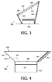
- Fig. 2 shows a light-emitting apparatus 200, comprising a semiconductor light-emitting device 220 and a ceramic wavelength converting body 230.
- the semiconductor device 220 has a light-emitting layer 221 disposed between an n-type region and a p-type region.
- the ceramic body 230 has a bottom surface 231 facing towards the semiconductor device 220 and oriented substantially parallel to the light-emitting layer 221. Furthermore, the ceramic body 230 has a top surface 232 and one or more side surfaces 233 at an oblique angle 234 with respect to the bottom surface 231 in order to enhance the light output from the body.
- the oblique angle 234 can either be sharp ( ⁇ 90°) or blunt (>90°).
- the 'primary' light 240 emitted by the light-emitting layer 221 is received and (at least partially) absorbed at a point 241 inside the ceramic wavelength converting body 230.
- the 'secondary' light 242 is radiated from point 241 over a solid angle of 4 ⁇ .
- the index of refraction of the ceramic body 230 is larger than 1, both the 'primary' 240 and 'secondary' light 242 are trapped inside the body due to total internal reflection, unless they are inside the escape cone.
- transparent bodies 230 i.e. which do not contain scattering centers such as pores or voids, the amount of light trapped in the waveguide modes is considerable.
- the ceramic wavelength converting body 230 is essentially adjacent to the semiconductor light-emitting device 220, it is to be understood that this is not essential for the invention. Also, the bottom surface 231 being parallel to the light-emitting layer 221 is not essential to the invention.
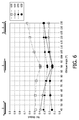
- the ceramic body 330 is positioned at a distance from the semiconductor device 320, albeit in light receiving relationship to that device. Such an embodiment is known as 'remote fluorescence' or 'remote phosphorescence'.
- the light emitted by the semiconductor device 320 is oriented towards the 'bottom' surface 331 of the ceramic wavelength converting body 330, directly and/or via any suitable optical system 360 known in the art.
- the light-emitting apparatus 300 can be advantageously used in applications such as general illuminators, recessed luminaires and even backlight units for displays. Furthermore, the apparatus 300 can be assembled such that the side surfaces 333 are either 'inside' (see Fig. 3 ) or 'outside' the optical system 360. In the later case, the light emitted from the side surfaces 333 can be advantageously used in appropriate lighting applications.
- the increase in light output of the apparatus 200, 300 by implementing the invention is considerable.
- an idealized rectangular transparent ceramic wavelength converting body 230, 330 of size 1x1x0.1 mm 3 , with an index of refraction of 1.8 (similar to YAG), surrounded by air (n 1) - geometry 1 in table 1.
- the geometry of the ceramic body 230,330 has on the light flux through and luminance of the top, side, and bottom surfaces.
- the loss of light i.e. the light unavailable for application, in the wave-guide modes (WGM), at the bottom surface, or at the side surfaces is considered.
- Geometry 1 is representative of a remote fluorescence example.
- the amount of light locked inside the waveguide modes is about 48%.
- every side of the rectangular body 230,330 emits an equal amount of light, it can be easily discerned that 8% of the light is emitted from the top surface 232,332 while the four side surfaces 233,333 emit 31 % of the light.
- a homogeneous translucent body is characterized by an equal brightness of every surface. Assuming furthermore that in practical circumstances the light emitted through the bottom surface 231 cannot be used, the total flux unavailable to the application is 57% (49%+8%).
- the ceramic body 230 is modeled to have a reflective bottom surface 231, with a reflection coefficient of 80%.
- This geometry is representative of a rectangular ceramic wavelength converting body 230 positioned adjacent to a semiconductor device 220. Although this geometry refers to a prior art embodiment, reference to the numbered elements of Fig. 2 is still made for the convenience of the reader.
- the light formerly locked in the wave-guide modes is essentially absorbed at the bottom surface 231, due to the multitude of 80% reflections occurring at this surface in the elongated rectangular 1x1x0.1 mm 3 body. Only a part of the light that was formerly emitted from the bottom surface 231 can now be emitted, after reflection, from the top surface 232 or the side surfaces 233. Overall 60% of the light generated inside the ceramic body 230 is not available in the lighting application.
- the total flux emitted from the ceramic body is considerably enhanced.
- the largest improvement is realized through unlocking the wave-guide modes via the top surface 232 of the ceramic body 230 (compare with geometry 1).
- the total flux available in a lighting application increases from 39% (8% top surface + 31% side surfaces) of the light generated to 88% (29% + 59%), again assuming that the flux through the bottom surface is not available.
- This geometry is especially suitable for lumen critical applications. These typically apply secondary optics appeasable to light received at large angles relative to their optical axis.
- the top surface 232 In order to enhance the brightness of the top surface 232 even further it is advantageous to apply a reflective coating to the oblique side surfaces 233 of the ceramic body 230, as in geometry 5.
- the reflective coating can be silver, aluminum or any other high reflective coating known in the art. Assuming an 80% reflectivity of the side surface coating the top surface 232 brightness increases twofold compared to geometry 2. This geometry is especially suitable for étendue critical applications.
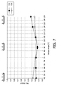
- a low index of refraction layer 451, i.e. n layer ⁇ n cer.body , between the side surfaces 433 and the reflective coating 452 is applied advantageously (see Fig. 4 ).
- the light outside the escape cone from the side surface 433 will be reflected through TIR with 100% efficiency.
- the light inside the escape cone will be reflected by the reflective coating 452, which in practical circumstances is always less efficient.
- applying the reflective coating 452 in direct optical contact with the side surfaces 433 will reduce the total reflective efficiency, as now also the light outside the escape cone is reflected less efficiently. Consequently, the application of the low index of reflection layer 451 enhances the flux emitted from the top surface 432 and its brightness even further (geometry 6 in table 1.)
- top surface 232,332,432 on a micro level to enhance the light extraction from and/or brightness of the top surface.
- a micro-corrugation can for example be created through etching of the top surface 232,332,432.
- the brightness of the top surface 232,332,432 is enhanced by corrugating that surface on a macro level, as for instance by shaping the top surface as a Fresnel lens, in order to include an optical function.
- This embodiment furthermore advantageously realizes an application specific radiation distribution from the light emitting apparatus 200,300,400.
- the ceramic body 230 can be advantageous to limit the light emitted form the ceramic body 230 to the side surfaces 233 only, as in geometry 7.
- An example of such an application is the use of the light-emitting apparatus 200 as a side emitter to couple light into a light-guide.
- the top surface 232 of the ceramic body 230 can be provided with a reflective coating 452 (with or without an intermediate low index of refraction layer 451).
- the ceramic wavelength converting body 230, 430 is positioned adjacent to a semiconductor device 220, 420 like the Philips Lumileds 'Saber'. These are so-called 'Flip Chip' InGaN based LEDs from which the sapphire substrate has been removed using e.g. laser lift-off techniques. This is especially advantageous as removing the 'intermediate' sapphire substrate will bring the ceramic body 230, 430 much closer to the light emitting layer 221, 421. Moreover, the absence of the sapphire substrate eliminates a loss-path of light generated in the body 230, 430. This loss-path would have been formed by light emitted through the bottom surface 231, 431 into the sapphire substrate and lost via the substrate's side surfaces.
- the light emission from the ceramic body 330 in a remote fluorescence application is shown as a function of the oblique angle 334.
- the body 330 is rectangular with equal size bottom 331 and top 332 surfaces.
- the bottom surface 331 is larger than the top surface 332.
- angles >90° it is advantageous to apply oblique angles 334 ⁇ 90°or >90° in order to enhance the bottom surface's flux 531, top surface's flux 532, side surfaces' flux 533, and total flux 530.
- the oblique angle 334 is ⁇ 85° or >95°, or even better ⁇ 80° or >100°.
- Fig. 6 shows the relative flux output and brightness of a ceramic wavelength conversion body 230 as a function of the oblique angle 234 for a flux critical application.
- Oblique angles 234 ⁇ 90° or >90° improve the total flux 630, the top surface's flux 632, and the side surfaces' flux 633 emitted.
- oblique angles 234 > 95° - or better still > 100° - are beneficially applied for flux critical applications.
- the top surface's brightness 635 (in Cd/mm 2 ), however, is beneficially improved for oblique angles 234 ⁇ 85°, or better still ⁇ 80°.
- Fig. 7 shows the relative output and brightness of a ceramic wavelength conversion body 430 as a function of the oblique angle 434 for an étendue critical application.
- the light can only be emitted through the top surface 432.
- Both the top surface's flux 732 and the top surface's brightness 735 are improved for oblique angles 434 ⁇ 90° and >90°, better still for angles ⁇ 85°and >95°.
- the top surface 432 has a smaller area for oblique angles ⁇ 90°. Consequently, the brightness 735 beneficially is enhanced for oblique angles 434 ⁇ 70°.
- Fig. 8 shows the relative output of a ceramic wavelength conversion body as a function of the oblique angle for a side emitter application.
- the flux 833 emitted from the side surfaces is beneficially improved for oblique angles ⁇ 90° and >90°.
- Varying the index of refraction difference between the ceramic body 230,330,430 and the surrounding medium will not substantially influence the dependence of the flux 530,532,630,632,732 emitted or the top surface brightness 635,735 on the oblique angle 234,334,434.
- the flux level is influenced, with an increase in flux for lower index of refraction differences.
Landscapes
- Physics & Mathematics (AREA)
- General Physics & Mathematics (AREA)
- Optics & Photonics (AREA)
- Led Device Packages (AREA)
Claims (6)
- Licht emittierende Vorrichtung (400), umfassend:- ein Licht emittierendes Halbleiterbauelement (420), das eine Licht emittierende Schicht (421) umfasst, die zwischen einer n-leitenden Region und einer p-leitenden Region angeordnet ist,- einen durchlässigen Keramikkörper (430), der ein Wellenlängenumwandlungsmaterial umfasst, das in Lichtempfangsbeziehung (430) mit dem Licht emittierenden Halbleiterbauelement positioniert ist,- wobei der Keramikkörper ferner eine Bodenfläche (431), die dem Licht emittierenden Halbleiterbauelement (420) gegenüberliegt, und eine Deckfläche (432) aufweist,dadurch gekennzeichnet, dass der Keramikkörper mindestens eine Seitenfläche (433) in einem schiefen Winkel (434) in Bezug auf die Bodenfläche aufweist, und wobei die mindestens eine schiefe Seitenfläche (433) des Keramikkörpers (430) eine reflektierende Beschichtung (452) aufweist, wobei eine Zwischenschicht (451) mit einem niedrigeren Brechungsindex als der Keramikkörper (430) zwischen dem Körper und der reflektierenden Beschichtung (452) untergebracht ist.
- Licht emittierende Vorrichtung nach Anspruch 1, wobei der schiefe Winkel größer als 95° oder kleiner als 85° ist.
- Licht emittierende Vorrichtung nach Anspruch 2, wobei der schiefe Winkel größer als 100° oder kleiner als 80° ist.
- Licht emittierende Vorrichtung nach einem der Ansprüche 1 bis 3, wobei der Keramikkörper (430) eine Deckfläche (432) aufweist, die mit einer Mikrowelligkeit versehen ist.
- Licht emittierende Vorrichtung nach einem der Ansprüche 1 bis 4, wobei der Keramikkörper (430) eine Deckfläche (432) aufweist, die so vorgesehen ist, dass sie eine optische Funktion umfasst.
- Licht emittierende Vorrichtung nach einem der vorhergehenden Ansprüche, wobei eine Zwischenschicht mit einem niedrigeren Brechungsindex als der Keramikkörper (430) zwischen der Bodenfläche (431) und dem Licht emittierenden Halbleiterbauelement (420) untergebracht ist.
Priority Applications (1)
| Application Number | Priority Date | Filing Date | Title |
|---|---|---|---|
| EP07849489.5A EP2097935B1 (de) | 2006-12-21 | 2007-12-14 | Lichtemissionsvorrichtung mit geformtem wellenlängenumrichter |
Applications Claiming Priority (3)
| Application Number | Priority Date | Filing Date | Title |
|---|---|---|---|
| EP06126787 | 2006-12-21 | ||
| EP07849489.5A EP2097935B1 (de) | 2006-12-21 | 2007-12-14 | Lichtemissionsvorrichtung mit geformtem wellenlängenumrichter |
| PCT/IB2007/055109 WO2008078235A2 (en) | 2006-12-21 | 2007-12-14 | Light-emitting apparatus with shaped wavelength converter |
Publications (2)
| Publication Number | Publication Date |
|---|---|
| EP2097935A2 EP2097935A2 (de) | 2009-09-09 |
| EP2097935B1 true EP2097935B1 (de) | 2016-10-05 |
Family
ID=39420349
Family Applications (1)
| Application Number | Title | Priority Date | Filing Date |
|---|---|---|---|
| EP07849489.5A Active EP2097935B1 (de) | 2006-12-21 | 2007-12-14 | Lichtemissionsvorrichtung mit geformtem wellenlängenumrichter |
Country Status (7)
| Country | Link |
|---|---|
| US (1) | US8410500B2 (de) |
| EP (1) | EP2097935B1 (de) |
| JP (1) | JP2010514187A (de) |
| KR (1) | KR101484461B1 (de) |
| CN (1) | CN101569020B (de) |
| TW (1) | TWI449206B (de) |
| WO (1) | WO2008078235A2 (de) |
Cited By (1)
| Publication number | Priority date | Publication date | Assignee | Title |
|---|---|---|---|---|
| WO2026037863A1 (en) * | 2024-08-14 | 2026-02-19 | Ams-Osram International Gmbh | Optoelectronic component |
Families Citing this family (31)
| Publication number | Priority date | Publication date | Assignee | Title |
|---|---|---|---|---|
| JP5226077B2 (ja) * | 2008-10-15 | 2013-07-03 | 株式会社小糸製作所 | 発光モジュール、発光モジュールの製造方法、および灯具ユニット |
| JPWO2010044239A1 (ja) * | 2008-10-17 | 2012-03-15 | 株式会社小糸製作所 | 発光モジュール、発光モジュールの製造方法、および灯具ユニット |
| JP5606922B2 (ja) * | 2008-11-28 | 2014-10-15 | 株式会社小糸製作所 | 発光モジュールおよび灯具ユニット |
| RU2535351C2 (ru) | 2009-05-28 | 2014-12-10 | Конинклейке Филипс Электроникс Н.В. | Устройство освещения и способ сборки устройства освещения |
| RU2538100C2 (ru) * | 2009-05-28 | 2015-01-10 | Конинклейке Филипс Электроникс Н.В. | Осветительное устройство с корпусом, заключающим в себе источник света |
| CN102449374B (zh) * | 2009-05-28 | 2016-05-11 | 皇家飞利浦电子股份有限公司 | 陶瓷照明设备 |
| US9300015B2 (en) | 2010-05-04 | 2016-03-29 | Dell Products Lp | Systems and methods for monitoring and characterizing information handling system use behavior |
| JP2012033823A (ja) | 2010-08-02 | 2012-02-16 | Stanley Electric Co Ltd | 発光装置およびその製造方法 |
| KR20120024104A (ko) * | 2010-09-06 | 2012-03-14 | 서울옵토디바이스주식회사 | 발광 소자 |
| CN102130108A (zh) * | 2010-12-14 | 2011-07-20 | 黄金鹿 | 一种透明陶瓷封装的led光源 |
| DE102011080179A1 (de) * | 2011-08-01 | 2013-02-07 | Osram Ag | Wellenlängenkonversionskörper und Verfahren zu dessen Herstellung |
| US9335017B2 (en) | 2011-12-20 | 2016-05-10 | Stanley Electric Co., Ltd. | Light emitting device that can realize reduction in thickness of vehicle light fitting, vehicle light fitting using the light emitting device and vehicle provided with the vehicle light |
| US10096742B2 (en) | 2012-03-28 | 2018-10-09 | Sensor Electronic Technology, Inc. | Light emitting device substrate with inclined sidewalls |
| US9595636B2 (en) | 2012-03-28 | 2017-03-14 | Sensor Electronic Technology, Inc. | Light emitting device substrate with inclined sidewalls |
| JP5816127B2 (ja) * | 2012-04-27 | 2015-11-18 | 株式会社東芝 | 半導体発光装置およびその製造方法 |
| WO2014030148A2 (en) * | 2012-08-24 | 2014-02-27 | Koninklijke Philips N.V. | A light emitting assembly, a lamp and a luminaire |
| DE102013204291A1 (de) * | 2013-03-12 | 2014-10-02 | Osram Opto Semiconductors Gmbh | Optoelektronisches Bauelement |
| DE102013206133B4 (de) | 2013-04-08 | 2021-09-30 | OSRAM Opto Semiconductors Gesellschaft mit beschränkter Haftung | Verfahren zum Herstellen eines Konversionselements und Konversionselement |
| DE102013107010A1 (de) * | 2013-07-03 | 2015-01-22 | Thyssenkrupp Steel Europe Ag | Anlage und Verfahren zum Warmwalzen von Stahlband |
| EP3020076B1 (de) | 2013-07-08 | 2017-09-06 | Koninklijke Philips N.V. | Wellenlängenumgewandeltes lichtemittierendes halbleiterbauelement |
| JP6694815B2 (ja) * | 2013-08-20 | 2020-05-20 | ルミレッズ ホールディング ベーフェー | 発光デバイス |
| JP2015056652A (ja) * | 2013-09-13 | 2015-03-23 | 株式会社東芝 | 窒化物半導体発光装置 |
| WO2015101535A1 (en) * | 2014-01-02 | 2015-07-09 | Koninklijke Philips N.V. | Light emitting device comprising releasable wavelength converter |
| WO2015104648A1 (en) * | 2014-01-09 | 2015-07-16 | Koninklijke Philips N.V. | Light emitting device with reflective sidewall |
| DE102014117440B3 (de) * | 2014-11-27 | 2016-04-07 | Seaborough IP IV BV | Lichtemittierende Remote-Phosphor-Vorrichtung |
| US9970629B2 (en) * | 2015-10-19 | 2018-05-15 | GE Lighting Solutions, LLC | Remote phosphor lighting devices and methods |
| CN107123713B (zh) * | 2016-02-25 | 2019-12-27 | 上海芯元基半导体科技有限公司 | 一种适合单色光led晶元级封装的器件结构 |
| US20180323354A1 (en) * | 2017-05-07 | 2018-11-08 | Yang Wang | Light emitting device and method for manufacturing light emitting device |
| US11296262B2 (en) | 2017-12-21 | 2022-04-05 | Lumileds Llc | Monolithic segmented LED array architecture with reduced area phosphor emission surface |
| DE102018200023A1 (de) * | 2018-01-02 | 2019-07-04 | Osram Gmbh | Konversionsvorrichtung mit geschichteter leiterstruktur |
| EP3831911B1 (de) * | 2019-12-05 | 2022-06-08 | Friedrich-Alexander-Universität Erlangen-Nürnberg | Verbundwellenlängenwandler |
Citations (2)
| Publication number | Priority date | Publication date | Assignee | Title |
|---|---|---|---|---|
| US20040211970A1 (en) * | 2003-04-24 | 2004-10-28 | Yoshiaki Hayashimoto | Semiconductor light emitting device with reflectors having cooling function |
| JP2006093399A (ja) * | 2004-09-24 | 2006-04-06 | Kyocera Corp | 発光装置およびその製造方法ならびに照明装置 |
Family Cites Families (23)
| Publication number | Priority date | Publication date | Assignee | Title |
|---|---|---|---|---|
| US3709827A (en) | 1970-02-10 | 1973-01-09 | F Auzel | Fluorescent materials for optical frequency conversion |
| US6229160B1 (en) * | 1997-06-03 | 2001-05-08 | Lumileds Lighting, U.S., Llc | Light extraction from a semiconductor light-emitting device via chip shaping |
| US6784463B2 (en) * | 1997-06-03 | 2004-08-31 | Lumileds Lighting U.S., Llc | III-Phospide and III-Arsenide flip chip light-emitting devices |
| US6429583B1 (en) | 1998-11-30 | 2002-08-06 | General Electric Company | Light emitting device with ba2mgsi2o7:eu2+, ba2sio4:eu2+, or (srxcay ba1-x-y)(a1zga1-z)2sr:eu2+phosphors |
| US6621211B1 (en) | 2000-05-15 | 2003-09-16 | General Electric Company | White light emitting phosphor blends for LED devices |
| DE10148227B4 (de) * | 2001-09-28 | 2015-03-05 | Osram Opto Semiconductors Gmbh | Strahlungsemittierender Halbleiterchip, Verfahren zu dessen Herstellung und strahlungsemittierendes Bauelement |
| US7554258B2 (en) | 2002-10-22 | 2009-06-30 | Osram Opto Semiconductors Gmbh | Light source having an LED and a luminescence conversion body and method for producing the luminescence conversion body |
| US7009213B2 (en) | 2003-07-31 | 2006-03-07 | Lumileds Lighting U.S., Llc | Light emitting devices with improved light extraction efficiency |
| JP2005079167A (ja) | 2003-08-28 | 2005-03-24 | Kyocera Corp | 発光素子収納用パッケージおよび発光装置 |
| JP4140042B2 (ja) | 2003-09-17 | 2008-08-27 | スタンレー電気株式会社 | 蛍光体を用いたled光源装置及びled光源装置を用いた車両前照灯 |
| DE10351397A1 (de) * | 2003-10-31 | 2005-06-16 | Osram Opto Semiconductors Gmbh | Lumineszenzdiodenchip |
| JP4604488B2 (ja) * | 2003-12-26 | 2011-01-05 | 日亜化学工業株式会社 | 窒化物半導体発光素子およびその製造方法 |
| JP3898721B2 (ja) * | 2004-01-28 | 2007-03-28 | 京セラ株式会社 | 発光装置および照明装置 |
| JP4020092B2 (ja) * | 2004-03-16 | 2007-12-12 | 住友電気工業株式会社 | 半導体発光装置 |
| US7361938B2 (en) * | 2004-06-03 | 2008-04-22 | Philips Lumileds Lighting Company Llc | Luminescent ceramic for a light emitting device |
| TW200614548A (en) * | 2004-07-09 | 2006-05-01 | Matsushita Electric Industrial Co Ltd | Light-emitting device |
| US20080093976A1 (en) * | 2004-09-23 | 2008-04-24 | Koninklijke Philips Electronics, N.V. | Light-Emitting Device |
| US20060091411A1 (en) * | 2004-10-29 | 2006-05-04 | Ouderkirk Andrew J | High brightness LED package |
| US8134292B2 (en) * | 2004-10-29 | 2012-03-13 | Ledengin, Inc. | Light emitting device with a thermal insulating and refractive index matching material |
| US7329982B2 (en) * | 2004-10-29 | 2008-02-12 | 3M Innovative Properties Company | LED package with non-bonded optical element |
| US7352011B2 (en) | 2004-11-15 | 2008-04-01 | Philips Lumileds Lighting Company, Llc | Wide emitting lens for LED useful for backlighting |
| JP4604763B2 (ja) * | 2005-02-24 | 2011-01-05 | ソニー株式会社 | バックライト装置及び液晶表示装置 |
| WO2006093011A1 (ja) * | 2005-03-01 | 2006-09-08 | Kabushiki Kaisha Toshiba | 発光装置 |
-
2007
- 2007-12-14 EP EP07849489.5A patent/EP2097935B1/de active Active
- 2007-12-14 JP JP2009542317A patent/JP2010514187A/ja active Pending
- 2007-12-14 KR KR1020097014974A patent/KR101484461B1/ko active Active
- 2007-12-14 US US12/519,439 patent/US8410500B2/en active Active
- 2007-12-14 WO PCT/IB2007/055109 patent/WO2008078235A2/en not_active Ceased
- 2007-12-14 CN CN200780047604XA patent/CN101569020B/zh active Active
- 2007-12-19 TW TW096148799A patent/TWI449206B/zh active
Patent Citations (2)
| Publication number | Priority date | Publication date | Assignee | Title |
|---|---|---|---|---|
| US20040211970A1 (en) * | 2003-04-24 | 2004-10-28 | Yoshiaki Hayashimoto | Semiconductor light emitting device with reflectors having cooling function |
| JP2006093399A (ja) * | 2004-09-24 | 2006-04-06 | Kyocera Corp | 発光装置およびその製造方法ならびに照明装置 |
Cited By (1)
| Publication number | Priority date | Publication date | Assignee | Title |
|---|---|---|---|---|
| WO2026037863A1 (en) * | 2024-08-14 | 2026-02-19 | Ams-Osram International Gmbh | Optoelectronic component |
Also Published As
| Publication number | Publication date |
|---|---|
| WO2008078235A2 (en) | 2008-07-03 |
| KR101484461B1 (ko) | 2015-01-20 |
| TW200836378A (en) | 2008-09-01 |
| US20100019265A1 (en) | 2010-01-28 |
| KR20090096630A (ko) | 2009-09-11 |
| TWI449206B (zh) | 2014-08-11 |
| JP2010514187A (ja) | 2010-04-30 |
| CN101569020A (zh) | 2009-10-28 |
| WO2008078235A3 (en) | 2008-08-21 |
| US8410500B2 (en) | 2013-04-02 |
| CN101569020B (zh) | 2011-05-18 |
| EP2097935A2 (de) | 2009-09-09 |
Similar Documents
| Publication | Publication Date | Title |
|---|---|---|
| EP2097935B1 (de) | Lichtemissionsvorrichtung mit geformtem wellenlängenumrichter | |
| US10074786B2 (en) | LED with scattering features in substrate | |
| CN107017241B (zh) | 发光装置 | |
| JP5482378B2 (ja) | 発光装置 | |
| JP5129437B2 (ja) | 発光ダイオード用光学システム | |
| CN103503178B (zh) | 光学元件以及利用了该光学元件的半导体发光装置 | |
| KR102000323B1 (ko) | 변환 소자 및 발광체 | |
| US10324247B2 (en) | Optical device for producing high brightness light | |
| CN109616567B (zh) | 发光装置 | |
| JP2010272847A5 (de) | ||
| KR20190010478A (ko) | 발광 장치, 집적형 발광 장치 및 발광 모듈 | |
| JP7328557B2 (ja) | 光源、光源装置および光源の製造方法 | |
| KR20230138023A (ko) | 광학 배열을 갖는 커버 구조를 갖는 발광 다이오드 패키지 및 제조 방법 | |
| WO2012011528A1 (ja) | 発光装置および照明装置 | |
| JP2016086166A (ja) | 発光装置 | |
| US20240027034A1 (en) | Light-emitting device | |
| CN109478587B (zh) | 用于生产光电子照明装置的方法和光电子照明装置 | |
| JP2025526835A (ja) | 固体発光コンポーネント | |
| JP2020053617A (ja) | 発光装置 | |
| KR102388371B1 (ko) | 반도체 소자 패키지 | |
| KR102145918B1 (ko) | 발광 소자 패키지 | |
| US20240213401A1 (en) | Textured lumiphore layer to improve light extraction for light-emitting diode chips and related methods | |
| US9356210B2 (en) | Optoelectronic module comprising an optical waveguide and method for producing same | |
| JP2023172001A (ja) | 波長変換部材及び発光装置並びに波長変換部材の製造方法 |
Legal Events
| Date | Code | Title | Description |
|---|---|---|---|
| PUAI | Public reference made under article 153(3) epc to a published international application that has entered the european phase |
Free format text: ORIGINAL CODE: 0009012 |
|
| 17P | Request for examination filed |
Effective date: 20090721 |
|
| AK | Designated contracting states |
Kind code of ref document: A2 Designated state(s): AT BE BG CH CY CZ DE DK EE ES FI FR GB GR HU IE IS IT LI LT LU LV MC MT NL PL PT RO SE SI SK TR |
|
| DAX | Request for extension of the european patent (deleted) | ||
| 17Q | First examination report despatched |
Effective date: 20100609 |
|
| RAP1 | Party data changed (applicant data changed or rights of an application transferred) |
Owner name: PHILIPS INTELLECTUAL PROPERTY & STANDARDS GMBH Owner name: KONINKLIJKE PHILIPS N.V. |
|
| REG | Reference to a national code |
Ref country code: DE Ref legal event code: R079 Ref document number: 602007048232 Country of ref document: DE Free format text: PREVIOUS MAIN CLASS: H01L0033000000 Ipc: H01L0033600000 |
|
| GRAP | Despatch of communication of intention to grant a patent |
Free format text: ORIGINAL CODE: EPIDOSNIGR1 |
|
| RIC1 | Information provided on ipc code assigned before grant |
Ipc: H01L 33/50 20100101ALI20160628BHEP Ipc: H01L 33/58 20100101ALN20160628BHEP Ipc: H01L 33/60 20100101AFI20160628BHEP |
|
| INTG | Intention to grant announced |
Effective date: 20160726 |
|
| GRAS | Grant fee paid |
Free format text: ORIGINAL CODE: EPIDOSNIGR3 |
|
| GRAA | (expected) grant |
Free format text: ORIGINAL CODE: 0009210 |
|
| AK | Designated contracting states |
Kind code of ref document: B1 Designated state(s): AT BE BG CH CY CZ DE DK EE ES FI FR GB GR HU IE IS IT LI LT LU LV MC MT NL PL PT RO SE SI SK TR |
|
| REG | Reference to a national code |
Ref country code: GB Ref legal event code: FG4D |
|
| REG | Reference to a national code |
Ref country code: CH Ref legal event code: EP |
|
| REG | Reference to a national code |
Ref country code: AT Ref legal event code: REF Ref document number: 835294 Country of ref document: AT Kind code of ref document: T Effective date: 20161015 |
|
| REG | Reference to a national code |
Ref country code: IE Ref legal event code: FG4D |
|
| REG | Reference to a national code |
Ref country code: DE Ref legal event code: R096 Ref document number: 602007048232 Country of ref document: DE |
|
| REG | Reference to a national code |
Ref country code: FR Ref legal event code: PLFP Year of fee payment: 10 |
|
| REG | Reference to a national code |
Ref country code: NL Ref legal event code: MP Effective date: 20161005 |
|
| REG | Reference to a national code |
Ref country code: LT Ref legal event code: MG4D |
|
| PG25 | Lapsed in a contracting state [announced via postgrant information from national office to epo] |
Ref country code: LV Free format text: LAPSE BECAUSE OF FAILURE TO SUBMIT A TRANSLATION OF THE DESCRIPTION OR TO PAY THE FEE WITHIN THE PRESCRIBED TIME-LIMIT Effective date: 20161005 |
|
| REG | Reference to a national code |
Ref country code: AT Ref legal event code: MK05 Ref document number: 835294 Country of ref document: AT Kind code of ref document: T Effective date: 20161005 |
|
| PG25 | Lapsed in a contracting state [announced via postgrant information from national office to epo] |
Ref country code: SE Free format text: LAPSE BECAUSE OF FAILURE TO SUBMIT A TRANSLATION OF THE DESCRIPTION OR TO PAY THE FEE WITHIN THE PRESCRIBED TIME-LIMIT Effective date: 20161005 Ref country code: GR Free format text: LAPSE BECAUSE OF FAILURE TO SUBMIT A TRANSLATION OF THE DESCRIPTION OR TO PAY THE FEE WITHIN THE PRESCRIBED TIME-LIMIT Effective date: 20170106 Ref country code: LT Free format text: LAPSE BECAUSE OF FAILURE TO SUBMIT A TRANSLATION OF THE DESCRIPTION OR TO PAY THE FEE WITHIN THE PRESCRIBED TIME-LIMIT Effective date: 20161005 |
|
| PG25 | Lapsed in a contracting state [announced via postgrant information from national office to epo] |
Ref country code: PL Free format text: LAPSE BECAUSE OF FAILURE TO SUBMIT A TRANSLATION OF THE DESCRIPTION OR TO PAY THE FEE WITHIN THE PRESCRIBED TIME-LIMIT Effective date: 20161005 Ref country code: ES Free format text: LAPSE BECAUSE OF FAILURE TO SUBMIT A TRANSLATION OF THE DESCRIPTION OR TO PAY THE FEE WITHIN THE PRESCRIBED TIME-LIMIT Effective date: 20161005 Ref country code: IS Free format text: LAPSE BECAUSE OF FAILURE TO SUBMIT A TRANSLATION OF THE DESCRIPTION OR TO PAY THE FEE WITHIN THE PRESCRIBED TIME-LIMIT Effective date: 20170205 Ref country code: FI Free format text: LAPSE BECAUSE OF FAILURE TO SUBMIT A TRANSLATION OF THE DESCRIPTION OR TO PAY THE FEE WITHIN THE PRESCRIBED TIME-LIMIT Effective date: 20161005 Ref country code: BE Free format text: LAPSE BECAUSE OF FAILURE TO SUBMIT A TRANSLATION OF THE DESCRIPTION OR TO PAY THE FEE WITHIN THE PRESCRIBED TIME-LIMIT Effective date: 20161005 Ref country code: NL Free format text: LAPSE BECAUSE OF FAILURE TO SUBMIT A TRANSLATION OF THE DESCRIPTION OR TO PAY THE FEE WITHIN THE PRESCRIBED TIME-LIMIT Effective date: 20161005 Ref country code: AT Free format text: LAPSE BECAUSE OF FAILURE TO SUBMIT A TRANSLATION OF THE DESCRIPTION OR TO PAY THE FEE WITHIN THE PRESCRIBED TIME-LIMIT Effective date: 20161005 Ref country code: PT Free format text: LAPSE BECAUSE OF FAILURE TO SUBMIT A TRANSLATION OF THE DESCRIPTION OR TO PAY THE FEE WITHIN THE PRESCRIBED TIME-LIMIT Effective date: 20170206 |
|
| REG | Reference to a national code |
Ref country code: DE Ref legal event code: R097 Ref document number: 602007048232 Country of ref document: DE |
|
| PG25 | Lapsed in a contracting state [announced via postgrant information from national office to epo] |
Ref country code: SK Free format text: LAPSE BECAUSE OF FAILURE TO SUBMIT A TRANSLATION OF THE DESCRIPTION OR TO PAY THE FEE WITHIN THE PRESCRIBED TIME-LIMIT Effective date: 20161005 Ref country code: RO Free format text: LAPSE BECAUSE OF FAILURE TO SUBMIT A TRANSLATION OF THE DESCRIPTION OR TO PAY THE FEE WITHIN THE PRESCRIBED TIME-LIMIT Effective date: 20161005 Ref country code: CZ Free format text: LAPSE BECAUSE OF FAILURE TO SUBMIT A TRANSLATION OF THE DESCRIPTION OR TO PAY THE FEE WITHIN THE PRESCRIBED TIME-LIMIT Effective date: 20161005 Ref country code: DK Free format text: LAPSE BECAUSE OF FAILURE TO SUBMIT A TRANSLATION OF THE DESCRIPTION OR TO PAY THE FEE WITHIN THE PRESCRIBED TIME-LIMIT Effective date: 20161005 Ref country code: EE Free format text: LAPSE BECAUSE OF FAILURE TO SUBMIT A TRANSLATION OF THE DESCRIPTION OR TO PAY THE FEE WITHIN THE PRESCRIBED TIME-LIMIT Effective date: 20161005 |
|
| REG | Reference to a national code |
Ref country code: CH Ref legal event code: PL |
|
| PLBE | No opposition filed within time limit |
Free format text: ORIGINAL CODE: 0009261 |
|
| STAA | Information on the status of an ep patent application or granted ep patent |
Free format text: STATUS: NO OPPOSITION FILED WITHIN TIME LIMIT |
|
| PG25 | Lapsed in a contracting state [announced via postgrant information from national office to epo] |
Ref country code: IT Free format text: LAPSE BECAUSE OF FAILURE TO SUBMIT A TRANSLATION OF THE DESCRIPTION OR TO PAY THE FEE WITHIN THE PRESCRIBED TIME-LIMIT Effective date: 20161005 Ref country code: BG Free format text: LAPSE BECAUSE OF FAILURE TO SUBMIT A TRANSLATION OF THE DESCRIPTION OR TO PAY THE FEE WITHIN THE PRESCRIBED TIME-LIMIT Effective date: 20170105 |
|
| 26N | No opposition filed |
Effective date: 20170706 |
|
| PG25 | Lapsed in a contracting state [announced via postgrant information from national office to epo] |
Ref country code: MC Free format text: LAPSE BECAUSE OF FAILURE TO SUBMIT A TRANSLATION OF THE DESCRIPTION OR TO PAY THE FEE WITHIN THE PRESCRIBED TIME-LIMIT Effective date: 20161005 |
|
| REG | Reference to a national code |
Ref country code: IE Ref legal event code: MM4A |
|
| PG25 | Lapsed in a contracting state [announced via postgrant information from national office to epo] |
Ref country code: CH Free format text: LAPSE BECAUSE OF NON-PAYMENT OF DUE FEES Effective date: 20161231 Ref country code: LI Free format text: LAPSE BECAUSE OF NON-PAYMENT OF DUE FEES Effective date: 20161231 Ref country code: LU Free format text: LAPSE BECAUSE OF NON-PAYMENT OF DUE FEES Effective date: 20161214 |
|
| PG25 | Lapsed in a contracting state [announced via postgrant information from national office to epo] |
Ref country code: SI Free format text: LAPSE BECAUSE OF FAILURE TO SUBMIT A TRANSLATION OF THE DESCRIPTION OR TO PAY THE FEE WITHIN THE PRESCRIBED TIME-LIMIT Effective date: 20161005 Ref country code: IE Free format text: LAPSE BECAUSE OF NON-PAYMENT OF DUE FEES Effective date: 20161214 |
|
| REG | Reference to a national code |
Ref country code: FR Ref legal event code: PLFP Year of fee payment: 11 |
|
| REG | Reference to a national code |
Ref country code: FR Ref legal event code: CA Effective date: 20180126 Ref country code: FR Ref legal event code: TP Owner name: LUMILEDS HOLDING B.V., NL Effective date: 20180126 |
|
| PG25 | Lapsed in a contracting state [announced via postgrant information from national office to epo] |
Ref country code: HU Free format text: LAPSE BECAUSE OF FAILURE TO SUBMIT A TRANSLATION OF THE DESCRIPTION OR TO PAY THE FEE WITHIN THE PRESCRIBED TIME-LIMIT; INVALID AB INITIO Effective date: 20071214 Ref country code: CY Free format text: LAPSE BECAUSE OF FAILURE TO SUBMIT A TRANSLATION OF THE DESCRIPTION OR TO PAY THE FEE WITHIN THE PRESCRIBED TIME-LIMIT Effective date: 20161005 |
|
| PG25 | Lapsed in a contracting state [announced via postgrant information from national office to epo] |
Ref country code: TR Free format text: LAPSE BECAUSE OF FAILURE TO SUBMIT A TRANSLATION OF THE DESCRIPTION OR TO PAY THE FEE WITHIN THE PRESCRIBED TIME-LIMIT Effective date: 20161005 |
|
| PG25 | Lapsed in a contracting state [announced via postgrant information from national office to epo] |
Ref country code: MT Free format text: LAPSE BECAUSE OF NON-PAYMENT OF DUE FEES Effective date: 20161214 |
|
| REG | Reference to a national code |
Ref country code: GB Ref legal event code: 732E Free format text: REGISTERED BETWEEN 20180920 AND 20180926 |
|
| REG | Reference to a national code |
Ref country code: DE Ref legal event code: R081 Ref document number: 602007048232 Country of ref document: DE Owner name: LUMILEDS HOLDING B.V., NL Free format text: FORMER OWNER: PHILIPS INTELLECTUAL PROPERTY & STANDARDS GMBH, 20099 HAMBURG, DE |
|
| P01 | Opt-out of the competence of the unified patent court (upc) registered |
Effective date: 20230530 |
|
| REG | Reference to a national code |
Ref country code: DE Ref legal event code: R079 Ref document number: 602007048232 Country of ref document: DE Free format text: PREVIOUS MAIN CLASS: H01L0033600000 Ipc: H10H0020856000 |
|
| PGFP | Annual fee paid to national office [announced via postgrant information from national office to epo] |
Ref country code: GB Payment date: 20251223 Year of fee payment: 19 |
|
| PGFP | Annual fee paid to national office [announced via postgrant information from national office to epo] |
Ref country code: FR Payment date: 20251230 Year of fee payment: 19 |
|
| PGFP | Annual fee paid to national office [announced via postgrant information from national office to epo] |
Ref country code: DE Payment date: 20251229 Year of fee payment: 19 |