EP2099054A2 - Spannungsregelungsvorrichtung, Stromversorgungsgerät, Elektronenröhre und Hochfrequenzschaltungssystem - Google Patents
Spannungsregelungsvorrichtung, Stromversorgungsgerät, Elektronenröhre und Hochfrequenzschaltungssystem Download PDFInfo
- Publication number
- EP2099054A2 EP2099054A2 EP09002964A EP09002964A EP2099054A2 EP 2099054 A2 EP2099054 A2 EP 2099054A2 EP 09002964 A EP09002964 A EP 09002964A EP 09002964 A EP09002964 A EP 09002964A EP 2099054 A2 EP2099054 A2 EP 2099054A2
- Authority
- EP
- European Patent Office
- Prior art keywords
- voltage
- electrode
- helix
- anode electrode
- twt
- Prior art date
- Legal status (The legal status is an assumption and is not a legal conclusion. Google has not performed a legal analysis and makes no representation as to the accuracy of the status listed.)
- Granted
Links
Images


Classifications
-
- H—ELECTRICITY
- H01—ELECTRIC ELEMENTS
- H01J—ELECTRIC DISCHARGE TUBES OR DISCHARGE LAMPS
- H01J23/00—Details of transit-time tubes of the types covered by group H01J25/00
- H01J23/34—Circuit arrangements not adapted to a particular application of the tube and not otherwise provided for
-
- H—ELECTRICITY
- H01—ELECTRIC ELEMENTS
- H01J—ELECTRIC DISCHARGE TUBES OR DISCHARGE LAMPS
- H01J25/00—Transit-time tubes, e.g. klystrons, travelling-wave tubes, magnetrons
- H01J25/34—Travelling-wave tubes; Tubes in which a travelling wave is simulated at spaced gaps
Definitions
- the present invention relates to a voltage control apparatus for controlling a direct voltage supplied to respective electrodes of an electron tube, a power supply apparatus and an electron tube having the voltage control apparatus, and a high-frequency circuit system having the same.
- a Traveling Wave Tube (TWT) or a klystron is an electron tube used for amplifying or oscillating a high-frequency signal through interaction between a beam of electrons emitted from an electron gun or the like and a high-frequency circuit.
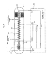
- a TWT 1 includes electron gun 10 for emitting a beam of electrons 50, helix electrode 20 functioning as a high-frequency circuit that allows a beam of electrons 50 emitted from electron gun 10 to interact with a high-frequency signal (i.e., a microwave signal), collector electrode 30 for collecting beam of electrons 50 emitted from helix electrode 20, and anode electrode 40 for drawing out electrons from electron gun 10 as well as guiding the beam of electrons 50 emitted from electron gun 10 into helix electrode 20.
- Electron gun 10 has cathode electrode 11 for emitting thermal electrons and heater 12 for supplying thermal energy for causing emission of the thermal electrons.
- the beam of electrons 50 emitted from electron gun 10 is accelerated by the electric potential difference between cathode electrode 11 and helix electrode 20 before entering helix electrode 20, and then travels inside helix electrode 20 while interacting with the high-frequency signal inputted through one end of helix electrode 20.
- collector electrode 30 captures the beam of electrons 50.
- the high-frequency signal, amplified through interaction with the beam of electrons 50 is outputted through the other end of helix electrode 20.
- Power supply apparatus 60 supplies a helix voltage E hel , which is a negative direct voltage based on the potential HELIX of helix electrode 20, to cathode electrode 11.
- power supply apparatus 60 supplies a collector voltage E col , which is a positive direct voltage based on the potential H/K of cathode electrode 11, to collector electrode 30, and supplies a heater voltage E h , which is a negative direct current based on the potential H/K of cathode electrode 11, to heater 12.
- helix electrode 20 is connected to a case of TWT 1 and is thereby grounded.
- FIG. 1 illustrates an example construction of TWT 1 having one collector electrode 30, TWT 1 may have a plurality of collector electrodes 30.
- FIG. 1 illustrates a construction in which anode electrode 40 and helix electrode 20 are connected inside power supply apparatus 60, it can be constructed such that anode electrode 40 is supplied with an anode voltage E a , which is a positive voltage with respect to the potential H/K of cathode electrode 11.
- Helix voltage E hel , collector voltage E col , and heater voltage E h are generated using, for example, a transformer, an inverter and a rectification circuit.
- the inverter serves to convert a direct voltage supplied from the outside into an alternating voltage and is connected to a first coil of the transformer.
- the rectification circuit serves to convert an alternating voltage outputted from a second coil of the transformer into a direct voltage.
- TWT 1 draws out electrons from cathode electrode 11 using the potential difference between anode electrode 40 and cathode electrode 11, it is preferable that the potential difference between anode electrode 40 and cathode electrode 11 be as small as possible in a state where an instable voltage is supplied to respective electrodes at the time when helix voltage E hel or collector voltage E col is raised (inputted).
- patent document 1 discloses a construction for controlling the supply and cutting-off of an anode voltage using a circuit, which is implemented with a Field Effect Transistor (FET).
- FET Field Effect Transistor
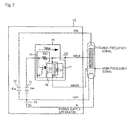
- FIG. 2 is a block diagram illustrating the construction of a high-frequency circuit system disclosed in patent document 1.
- the high-frequency circuit system disclosed in patent document 1 includes transistor Q1 and a transistor Q2 provided for on/off control of transistor Q1.
- transistor Q1 a source is connected to a cathode electrode of TWT 1 and a drain is connected to a helix electrode via anode electrode A of TWT 1 and via resistor R1.
- transistor Q1 is an N-channel FET
- transistor Q2 is an N-channel Metal-Oxide Semiconductor FET (MOSFET).
- MOSFET Metal-Oxide Semiconductor FET
- Tansistor Q1 has a gate connected to a drain of transistor Q2, and resistor R2 is connected in parallel between the gate and the source of transistor Q1.
- Transistor Q2 has a source connected to a heater of TWT 1.
- a gate of transistor Q2 is applied with a voltage, which is obtained by dividing a voltage between the helix electrode and the heater of TWT 1 using resistors R3 and R4.
- transistor Q1 in a time period when helix voltage E hel and collector voltage E col are being raised (i.e., inputted), transistor Q1 is switched on so that the potential of anode electrode A is substantially identical with the potential of cathode electrode H/K.
- transistor Q1 is switched off so that the potential of anode electrode A is substantially identical with ground potential HELIX. Timing to switch transistor Q1 from “on” to “off” is determined by the voltage division ratio between resistors R3 and R4 connected to the gate of transistor Q2.
- patent documents 2 through 4 disclose a construction in which resistors R11 and R12 are connected in series between the helix electrode and the cathode electrode of TWT 1, and resistors R11 and R12 supply a voltage obtained by dividing helix voltage E hel .
- resistor R1 For example, if a current flowing through the anode electrode in the normal operation of TWT 1 is 0.1 mA and if the resistance of resistor R1 is 10 M ⁇ , the potential of the anode electrode decreases by 1 kV compared to the potential of the helix electrode. If the resistance of resistor R1 is reduced, the potential difference between the anode electrode and the helix electrode can be reduced in the normal operation.
- resistor R1 requires a large amount of rated power since it consumes a large amount of power due to helix voltage E hel that is applied when transistor Q1 is on.
- a voltage obtained by dividing helix voltage E hel using resistors R11 and R12 is applied to anode electrode A when TWT 1 performs a normal operation. Accordingly, as a drawback, the anode voltage is reduced in the normal operation of TWT 1, thereby decreasing the maximum gain of TWT 1.
- the object of the present invention to provide a voltage control apparatus, which can prevent an excessive amount of current from flowing through a helix electrode when a helix voltage and a collector voltage are raised so as to prevent an electron tube such as a Traveling Wave Tube (TWT) from deterioration or damage as well as to reduce the load on a power supply apparatus without reducing the maximum gain in normal operation of the electron tube, and also to provide a power supply apparatus and an electron tube having the voltage control apparatus, and a high-frequency circuit system having the same.
- TWT Traveling Wave Tube
- a voltage control apparatus used for an electron tube, which includes at least an anode electrode, a cathode electrode and a helix electrode.
- the voltage control apparatus may include a detecting circuit for detecting a current flowing through the helix electrode; a voltage-limiting circuit for controlling a potential difference between the electrode and the anode electrode based on a predetermined voltage level; and a switch for connecting the helix electrode and the anode electrode through the voltage-limiting circuit or for causing a short circuit between the helix electrode and the anode electrode based on the output from the detecting circuit.
- a power supply apparatus including the above-described voltage control apparatus.
- an electron tube including the above-described voltage control apparatus.
- a high-frequency circuit system may include: the above-described power supply apparatus; and an electron tube in which a direct voltage from the power supply apparatus is supplied to an anode electrode, a cathode electrode and a helix electrode.
- the high-frequency circuit system may include: the above-described electron tube; and a power supply apparatus for supplying a direct voltage to an anode electrode, a cathode electrode and a helix electrode of the electron tube.
- TWT Traveling Wave Tube
- the present invention can also be applied to any construction in which a direct voltage is applied to respective electrodes in different types of electron tube.
- FIG. 5 is a circuit diagram illustrating the construction of a voltage control apparatus according to a first exemplary embodiment of the invention.
- Voltage control apparatus 74 illustrated in FIG. 5 is constructed to reduce helix current I HELIX , i.e., a current flowing through the helix electrode of TWT 1 (see FIG. 7 ) by restraining an anode voltage in response to the detection of an increase in helix current I HELIX when helix voltage E hel and collector voltage E col are inputted to TWT 1.
- I HELIX helix current flowing through the helix electrode of TWT 1 (see FIG. 7 )
- voltage control apparatus 74 includes detecting circuit 75, switch 76 and voltage-limiting circuit 77.
- Detecting circuit 75 is connected between a helix power source generating helix voltage E hel and the helix electrode of TWT 1 (see FIG. 7 ) to detect helix current I HELIX flowing through the helix electrode of TWT 1, as well as to perform on/off control on switch 76. Detecting circuit 75 turns on switch 76 when helix current I HELIX does not exceed a predetermined threshold, but turns off switch 76 when helix current I HELIX exceeds the threshold.
- Switch 76 is connected between the helix electrode and an anode electrode of TWT 1 (see FIG. 7 ) and is turned on/off according to an output signal from detecting circuit 75 to connect the helix electrode and the anode electrode through voltage-limiting circuit 77 or to cause a short circuit between the helix electrode and the anode electrode.
- Voltage-limiting circuit 77 is connected between the helix electrode and the anode electrode of TWT 1 (see FIG. 7 ), and when switch 76 is turned off, controls the potential difference between the helix electrode and the anode electrode based on a predetermined value.
- FIG. 6 is a block diagram illustrating the construction of a power supply apparatus including the voltage control apparatus shown in FIG. 5 .
- power supply apparatus 70 includes helix power source 71 for generating helix voltage E hel supplied to TWT 1 (see FIG. 7 ), collector power source 72 for generating collector voltage E col , heater power source 73 for generating heater voltage E h and power control apparatus 74 shown in FIG. 5 .
- detecting circuit 75 has one end connected to helix power source 71 and the other end connected to the helix electrode of TWT 1 (see FIG. 7 ). The other end of detecting circuit 75 is grounded inside power supply apparatus 70.
- Switch 76 and voltage-limiting circuit 77 of power control apparatus 74 are connected between the helix electrode and the anode electrode of TWT 1 (see FIG. 7 ).
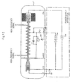
- FIG. 7 is a block diagram illustrating the construction of a high-frequency circuit system according to the first exemplary embodiment.
- the high-frequency circuit system includes TWT 1 and power supply apparatus 70 (shown in FIG. 6 ) for supplying a direct voltage (i.e., a supply voltage) to respective electrodes of TWT 1. Since TWT 1 shown in FIG. 7 has substantially the same construction as TWT 1 of the related art shown in FIG. 1 , a description thereof will be omitted.
- Power supply apparatus 70 supplies helix voltage E hel from helix power source 71 to a cathode electrode of TWT 1 through voltage control apparatus 74.
- power supply apparatus 70 supplies collector voltage E col from collector power source 72 to the collector electrode of TWT 1, where collector voltage E col is a positive voltage with respect to the potential H/K of the cathode electrode, and supplies a heater electrode E h from heater power source 73 to a heater of TWT 1, where the heater electrode E h is a negative voltage with respect to the potential H/K of the cathode electrode.
- the collector electrode and the heater of TWT 1 shown in FIG. 7 When a predetermined amount of voltage is supplied from power supply apparatus 70 to the cathode electrode, the collector electrode and the heater of TWT 1 shown in FIG. 7 , it emits a beam of electrons from the cathode electrode to the collector electrode and outputs a high-frequency signal inputted to the helix electrode by amplifying the high-frequency signal through the interaction between the high-frequency signal and the beam of electrons.
- voltage control circuit 77 of this exemplary embodiment uses Zener diode D1 that limits the potential difference between the helix electrode and anode electrode A within the Zener voltage.
- Zener diode D1 has a cathode connected to the helix electrode of TWT 1 and an anode connected to anode electrode A of TWT 1.
- Switch 76 of voltage control apparatus 74 is implemented with transistor Q11 made of a P-channel Metal-Oxide Semiconductor Field Emission Transistor (MOSFET).
- Transistor Q11 has a source connected to the helix electrode of TWT 1 and a drain connected to anode electrode A of TWT 1.
- MOSFET Metal-Oxide Semiconductor Field Emission Transistor
- Detecting circuit 75 includes direct voltage source 80 for supplying a negative direct voltage to the gate of transistor Q11 and current-detecting resistor R21 connected between the source of transistor Q11 and direct voltage source 80.
- Direct voltage source 80 has a positive electrode connected to helix power source 71 and a negative electrode connected to the gate of transistor Q11. When TWT 1 performs a normal operation, direct voltage source 80 outputs a constant direct voltage, which turns on transistor Q11. The level of the voltage from direct voltage source 80 is a threshold for determining the turning on or off of transistor Q11 (of the switch 76). Direct voltage source 80 can be implemented with a power circuit well-known in the art, and can be implemented with any circuits as long as they can generate and output a constant direct voltage.
- Current-detecting resistor R21 has one end connected to the source of transistor Q11 and the other end connected to helix power source 71, and generates a potential difference according to helix current I HELIX .
- the potential difference causes a voltage, applied from direct voltage source 80 to the gate of transistor Q11, to drop below the operating voltage of transistor Q11 (i.e., to drop to a voltage level at which transistor Q11 is turned off). That is, detecting circuit 75 turns on transistor Q11 (switch 76) when helix current I HELIX does not exceed a predetermined threshold but turns off transistor Q11 (switch 76) when helix current I HELIX exceeds the threshold.
- FIG. 8 is a schematic diagram illustrating changes in helix voltage, anode voltage and helix current, which are raised by a power supply apparatus according to the first exemplary embodiment.
- the characteristics of the anode voltage and the helix voltage schematically represent changes in the voltages based on the potential H/K of the cathode electrode but are not actual voltage values.
- direct voltage source 80 outputs a predetermined constant level of direct voltage before helix voltage E hel and collector voltage E col are inputted.
- the anode electrode of TWT 1 has substantially the same potential as that of the helix electrode (i.e., a ground potential GND) and thereby prevents the maximum gain of TWT 1 from decreasing in normal operation.
- direct voltage source 80 applies a constant negative level of direct voltage with respect to the potential of the positive electrode of helix power source 71 to the gate of transistor Q11, a potential difference occurs between the both ends of current-detecting resistor R21 which raises the potential of the positive electrode of direct voltage source 80 while lowering the potential difference between the source and the gate of transistor Q11.
- helix current I HELIX is enhanced to increase the potential difference between the both ends of current-detecting resistor R21.
- transistor Q11 is turned off.
- a voltage applied to anode electrode A of TWT 1 is limited to a voltage level, which is lowered from the potential of the helix electrode by the Zener voltage of Zener diode D1 (in the direction of the potential H/K of the cathode electrode). Therefore, as shown in FIG. 8 , helix current I HELIX is reduced since the anode voltage is limited in the case where helix voltage E hel and collector voltage E col are inputted.
- transistor Q11 When helix voltage E hel and collector voltage E col reach a predetermined voltage level and the reduced helix current I HELIX decreases the potential difference between the both ends of current-detecting resistor R21, transistor Q11 is turned on to cause a short circuit between the anode electrode and the helix electrode of TWT 1.
- helix current I HELIX that flows while helix voltage E hel and collector voltage E col are raised is reduced compared to the related art illustrated in FIG. 1 since the anode voltage is restrained by Zener diode D1 (i.e., current-limiting circuit 77) connected between the helix electrode and the anode electrode.
- Zener diode D1 i.e., current-limiting circuit 77
- the reduced helix current also decreases the load on power supply apparatus 70 associated with inputting helix voltage E hel and collector voltage E col .
- the anode voltage is controlled using Zener diode D1 and transistor Q11, a simple construction consisting of commonly used, inexpensive parts can be used to reduce helix current I HELIX in the case where helix voltage E hel and collector voltage E col are inputted. Therefore, it is possible to prevent the cost of the high-frequency circuit system from rising.
- FIG. 7 illustrates an exemplary construction in which switch 76 connected between the helix electrode and the anode electrode of TWT 1 is implemented with transistor Q11
- switch 76 can be implemented with a relay as shown in FIG. 9 .
- FIG. 9 illustrates an exemplary construction in which a switch part of relay 81 is connected between the helix electrode and the anode electrode of TWT 1 and a drive part for driving the switch part is connected between the negative electrode of direct voltage source 80 and the positive electrode of helix power source 71.
- an output voltage from direct voltage source 80 is set to such a voltage level that turns on the switch part of relay 81 when TWT 1 performs a normal operation but turns off the switch part of relay 81 (that is, causes relay 81 to be below an operating voltage) due to the potential difference generated from current-detecting resistor R21 when an excessive amount of helix current I HELIX flows.
- FIG. 10 is a block diagram illustrating the construction of a high-frequency circuit system according to a second exemplary embodiment.
- power supply apparatus 70 includes resistors (voltage division resistors) R31 and R32, connected in series between the helix electrode and the cathode electrode of TWT 1, as voltage-limiting circuit 77 of voltage control apparatus 74.
- Power supply apparatus 70 is constructed to supply a division voltage, obtained by dividing helix voltage E hel using voltage division resistors R31 and R32, to anode electrode A. Since the other features of voltage control apparatus 74 and the constructions of power supply apparatus 70 and the high-frequency circuit system are substantially the same as those of the first exemplary embodiment, descriptions thereof will be omitted.
- FIG. 10 illustrates an exemplary construction in which helix voltage E hel is divided using the voltage division resistors R31 and R32 connected in series
- the number of the voltage division resistors is not limited as long as helix voltage E hel can be divided before being supplied to anode electrode A.
- helix current I HELIX is reduced compared to the related art illustrated in FIG. 1 since the anode voltage is restrained by voltage division resistors R31 and R32 (of voltage-limiting circuit 77) that are connected between the helix electrode and anode electrode. As a result, this can prevent TWT 1 from deterioration or damage.
- the reduced helix current also decreases the load on power supply apparatus 70 associated with inputting helix voltage E hel and collector voltage E col .
- the anode voltage is controlled using voltage division resistors R31 and R32 and transistor Q11, a simple construction consisting of commonly used, inexpensive parts can be used to reduce helix current I HELIX in the case where helix voltage E hel and collector voltage E col are inputted. Therefore, it is possible to prevent the cost of the high-frequency circuit system from rising.
- FIG. 11 is a block diagram illustrating the construction of a TWT having the voltage control apparatus shown in FIG. 5 .
- voltage control apparatus 74 is provided in power supply apparatus 70.
- the third exemplary embodiment is constructed such that voltage control apparatus 74 disclosed in the first and second exemplary embodiments is provided in TWT 1.
- detecting circuit 75 of voltage control apparatus 74 has one end connected to the helix electrode and the other end connected to the helix power source of a power supply apparatus (not shown).
- the helix electrode is connected to the case of TWT 1 and is thereby grounded.
- switch 76 and voltage-limiting circuit 77 of voltage control apparatus 74 are connected between the helix electrode and anode electrode of TWT 1. Since operation of voltage control apparatus 74 shown in FIG. 11 is substantially the same as those of the first and second exemplary embodiment, a description thereof will be omitted.
- FIGS. 12 and 13 are block diagrams illustrating exemplary constructions of a high-frequency circuit system according to a third exemplary.
- FIG. 12 illustrates an exemplary construction in which voltage control apparatus 74 of the first exemplary embodiment shown in FIG. 7 is provided in TWT 1
- FIG. 13 illustrates another exemplary construction in which voltage control apparatus 74 of the second exemplary embodiment shown in FIG. 10 is provided in TWT 1.
- TWT 1 may be provided with voltage control apparatus 74 shown in FIG. 9 . Since the other features and the operation of TWT 1 and the construction and operation of power supply apparatus 70 are substantially the same as those of the related art illustrated in FIG. 1 , descriptions thereof will be omitted.
- the third exemplary embodiment having voltage control apparatus 74 provided in TWT 1 can obtain the same effects as those that are obtained in the high-frequency circuit system of the first and second exemplary embodiments.
Landscapes
- Microwave Tubes (AREA)
Applications Claiming Priority (1)
| Application Number | Priority Date | Filing Date | Title |
|---|---|---|---|
| JP2008051951A JP5136892B2 (ja) | 2008-03-03 | 2008-03-03 | 電圧制御装置、電源装置、電子管及び高周波回路システム |
Publications (3)
| Publication Number | Publication Date |
|---|---|
| EP2099054A2 true EP2099054A2 (de) | 2009-09-09 |
| EP2099054A3 EP2099054A3 (de) | 2010-07-14 |
| EP2099054B1 EP2099054B1 (de) | 2011-07-06 |
Family
ID=40481965
Family Applications (1)
| Application Number | Title | Priority Date | Filing Date |
|---|---|---|---|
| EP09002964A Active EP2099054B1 (de) | 2008-03-03 | 2009-03-02 | Spannungsregelungsvorrichtung, Stromversorgungsgerät, Elektronenröhre und Hochfrequenzschaltungssystem |
Country Status (3)
| Country | Link |
|---|---|
| US (1) | US8212481B2 (de) |
| EP (1) | EP2099054B1 (de) |
| JP (1) | JP5136892B2 (de) |
Cited By (2)
| Publication number | Priority date | Publication date | Assignee | Title |
|---|---|---|---|---|
| EP2775612A1 (de) * | 2013-03-08 | 2014-09-10 | Tesat-Spacecom GmbH & Co. KG | Verfahren zum Betreiben eines Wanderfeldröhrenmoduls |
| US10992272B2 (en) | 2018-11-15 | 2021-04-27 | Tesat-Spacecom Gmbh & Co. Kg | High-frequency module with connection interface |
Families Citing this family (7)
| Publication number | Priority date | Publication date | Assignee | Title |
|---|---|---|---|---|
| JP5099636B2 (ja) * | 2008-03-19 | 2012-12-19 | 株式会社ネットコムセック | 電流測定装置、電圧測定装置及びそれを備えた電源装置 |
| EP2445103A1 (de) * | 2010-10-22 | 2012-04-25 | Thales | Leistungsverwaltungssystem für Dual-Wanderfeldröhrenverstärker |
| JP6300312B2 (ja) | 2013-03-29 | 2018-03-28 | Necネットワーク・センサ株式会社 | 進行波管システム |
| JP6409296B2 (ja) * | 2014-03-19 | 2018-10-24 | 日本電気株式会社 | 送信機、レーダ装置及び送信電力制御方法 |
| US9927317B2 (en) * | 2015-07-09 | 2018-03-27 | Mks Instruments, Inc. | Ionization pressure gauge with bias voltage and emission current control and measurement |
| WO2017051528A1 (ja) * | 2015-09-24 | 2017-03-30 | Necネットワーク・センサ株式会社 | 電子銃、電子管及び高周波回路システム |
| US11664184B2 (en) * | 2019-07-09 | 2023-05-30 | Varex Imaging Corporation | Electron gun driver |
Citations (4)
| Publication number | Priority date | Publication date | Assignee | Title |
|---|---|---|---|---|
| JPS57186966U (de) | 1981-05-22 | 1982-11-27 | ||
| JPS61157251U (de) | 1985-03-23 | 1986-09-29 | ||
| JPH0476240U (de) | 1990-11-14 | 1992-07-03 | ||
| JP2005093229A (ja) | 2003-09-17 | 2005-04-07 | Nec Microwave Inc | 進行波管用電源供給回路、進行波管装置、および進行波管用電源装置 |
Family Cites Families (15)
| Publication number | Priority date | Publication date | Assignee | Title |
|---|---|---|---|---|
| JPS494564Y1 (de) * | 1969-08-23 | 1974-02-02 | ||
| JPS52129303A (en) * | 1976-04-23 | 1977-10-29 | Nec Corp | High-voltage power source unit for super high frequency electronic tube |
| JPS5391602A (en) * | 1977-01-24 | 1978-08-11 | Nec Corp | Power unit for micro wave electron tube |
| JPS55113239A (en) * | 1979-02-23 | 1980-09-01 | Nec Corp | Power source device for traveling-wave tube |
| JPS57186966A (en) | 1981-05-11 | 1982-11-17 | Hitachi Ltd | Rotor for permanent-magnet type synchronous motor |
| JPH0422534Y2 (de) * | 1984-11-19 | 1992-05-22 | ||
| JPS61157251A (ja) * | 1984-12-28 | 1986-07-16 | Secoh Giken Inc | 往復して負荷を振動する装置 |
| JPH02142029A (ja) * | 1988-11-22 | 1990-05-31 | Toshiba Corp | 電子管の保護装置 |
| JP2864681B2 (ja) * | 1990-07-19 | 1999-03-03 | 三菱自動車工業株式会社 | 内燃エンジンの空燃比制御方法 |
| US5952740A (en) * | 1994-05-12 | 1999-09-14 | Komatsu Ltd. | Load drive device |
| US5500621A (en) * | 1995-04-03 | 1996-03-19 | Martin Marietta Corp. | Travelling-wave tube protection arrangement |
| JP3970658B2 (ja) * | 2002-03-29 | 2007-09-05 | Necマイクロ波管株式会社 | マイクロ波管用電源装置 |
| JP2005116355A (ja) * | 2003-10-08 | 2005-04-28 | Nec Microwave Inc | マイクロ波管システム及びマイクロ波管 |
| JP4796855B2 (ja) * | 2006-01-31 | 2011-10-19 | 株式会社ネットコムセック | 電源装置及び高周波回路システム |
| JP5158585B2 (ja) * | 2007-10-12 | 2013-03-06 | 株式会社ネットコムセック | 電源装置及び高周波回路システム |
-
2008
- 2008-03-03 JP JP2008051951A patent/JP5136892B2/ja active Active
-
2009
- 2009-03-02 EP EP09002964A patent/EP2099054B1/de active Active
- 2009-03-02 US US12/395,994 patent/US8212481B2/en active Active
Patent Citations (4)
| Publication number | Priority date | Publication date | Assignee | Title |
|---|---|---|---|---|
| JPS57186966U (de) | 1981-05-22 | 1982-11-27 | ||
| JPS61157251U (de) | 1985-03-23 | 1986-09-29 | ||
| JPH0476240U (de) | 1990-11-14 | 1992-07-03 | ||
| JP2005093229A (ja) | 2003-09-17 | 2005-04-07 | Nec Microwave Inc | 進行波管用電源供給回路、進行波管装置、および進行波管用電源装置 |
Cited By (3)
| Publication number | Priority date | Publication date | Assignee | Title |
|---|---|---|---|---|
| EP2775612A1 (de) * | 2013-03-08 | 2014-09-10 | Tesat-Spacecom GmbH & Co. KG | Verfahren zum Betreiben eines Wanderfeldröhrenmoduls |
| US9530604B2 (en) | 2013-03-08 | 2016-12-27 | Tesat-Spacecom Gmbh & Co. Kg | Method for operating a traveling-wave tube module |
| US10992272B2 (en) | 2018-11-15 | 2021-04-27 | Tesat-Spacecom Gmbh & Co. Kg | High-frequency module with connection interface |
Also Published As
| Publication number | Publication date |
|---|---|
| EP2099054A3 (de) | 2010-07-14 |
| JP5136892B2 (ja) | 2013-02-06 |
| JP2009211872A (ja) | 2009-09-17 |
| US20090218948A1 (en) | 2009-09-03 |
| EP2099054B1 (de) | 2011-07-06 |
| US8212481B2 (en) | 2012-07-03 |
Similar Documents
| Publication | Publication Date | Title |
|---|---|---|
| EP2099054B1 (de) | Spannungsregelungsvorrichtung, Stromversorgungsgerät, Elektronenröhre und Hochfrequenzschaltungssystem | |
| JP5158585B2 (ja) | 電源装置及び高周波回路システム | |
| EP1862879B1 (de) | Linearer Hochspannungsregler für Elektronenröhren | |
| EP1814134B1 (de) | Stromversorgungsgerät und Hochfrequenzschaltkreissystem | |
| JP5216270B2 (ja) | 高電圧スイッチ制御回路とそれを用いたx線装置 | |
| CN106329916B (zh) | 开关管的驱动方法及电路及电源系统 | |
| JP2008235997A (ja) | スイッチング回路 | |
| US11676752B2 (en) | Systems and methods to safely discharge inductors without energy limitations | |
| CN112534668B (zh) | 升压转换器短路保护 | |
| US9093837B2 (en) | Abnormal voltage detecting device | |
| US8446207B2 (en) | Load driving circuit | |
| JP2016220367A (ja) | 放電装置 | |
| CN101552598B (zh) | 切换式功率晶体管的栅极驱动电路 | |
| CN108233701B (zh) | 一种升降压电压转换电路 | |
| CN107404217B (zh) | 开关电源控制电路和方法及开关电源 | |
| JP2000298152A (ja) | 故障検出装置 | |
| CN115776230A (zh) | 高压电源装置 | |
| EP2662554A1 (de) | Treiberschaltung für ein Magnetventil | |
| JP5369987B2 (ja) | ゲート駆動回路 | |
| JP5789427B2 (ja) | ドライブ回路 | |
| JP5880502B2 (ja) | 電気負荷駆動装置 | |
| JP2011229327A (ja) | スイッチング制御回路 | |
| CN120064352A (zh) | 荧光x射线分析装置和电源装置 | |
| CN119766212A (zh) | 一种开关功率管截止控制电路及驱动芯片 | |
| CN121239211A (zh) | 一种具有单电源负压关断的栅极驱动器 |
Legal Events
| Date | Code | Title | Description |
|---|---|---|---|
| PUAI | Public reference made under article 153(3) epc to a published international application that has entered the european phase |
Free format text: ORIGINAL CODE: 0009012 |
|
| AK | Designated contracting states |
Kind code of ref document: A2 Designated state(s): AT BE BG CH CY CZ DE DK EE ES FI FR GB GR HR HU IE IS IT LI LT LU LV MC MK MT NL NO PL PT RO SE SI SK TR |
|
| AX | Request for extension of the european patent |
Extension state: AL BA RS |
|
| PUAL | Search report despatched |
Free format text: ORIGINAL CODE: 0009013 |
|
| AK | Designated contracting states |
Kind code of ref document: A3 Designated state(s): AT BE BG CH CY CZ DE DK EE ES FI FR GB GR HR HU IE IS IT LI LT LU LV MC MK MT NL NO PL PT RO SE SI SK TR |
|
| AX | Request for extension of the european patent |
Extension state: AL BA RS |
|
| RAP1 | Party data changed (applicant data changed or rights of an application transferred) |
Owner name: NETCOMSEC CO., LTD |
|
| GRAP | Despatch of communication of intention to grant a patent |
Free format text: ORIGINAL CODE: EPIDOSNIGR1 |
|
| 17P | Request for examination filed |
Effective date: 20110114 |
|
| RIC1 | Information provided on ipc code assigned before grant |
Ipc: H01J 25/34 20060101ALI20110209BHEP Ipc: H01J 23/34 20060101AFI20110209BHEP |
|
| RTI1 | Title (correction) |
Free format text: VOLTAGE CONTROL APPARATUS, POWER SUPPLY APPARATUS, ELECTRON TUBE AND HIGH-FREQUENCY CIRCUIT SYSTEM |
|
| AKX | Designation fees paid |
Designated state(s): DE FR GB |
|
| GRAS | Grant fee paid |
Free format text: ORIGINAL CODE: EPIDOSNIGR3 |
|
| GRAA | (expected) grant |
Free format text: ORIGINAL CODE: 0009210 |
|
| AK | Designated contracting states |
Kind code of ref document: B1 Designated state(s): DE FR GB |
|
| REG | Reference to a national code |
Ref country code: GB Ref legal event code: FG4D |
|
| REG | Reference to a national code |
Ref country code: DE Ref legal event code: R096 Ref document number: 602009001703 Country of ref document: DE Effective date: 20110901 |
|
| PLBE | No opposition filed within time limit |
Free format text: ORIGINAL CODE: 0009261 |
|
| STAA | Information on the status of an ep patent application or granted ep patent |
Free format text: STATUS: NO OPPOSITION FILED WITHIN TIME LIMIT |
|
| 26N | No opposition filed |
Effective date: 20120411 |
|
| REG | Reference to a national code |
Ref country code: DE Ref legal event code: R097 Ref document number: 602009001703 Country of ref document: DE Effective date: 20120411 |
|
| REG | Reference to a national code |
Ref country code: DE Ref legal event code: R082 Ref document number: 602009001703 Country of ref document: DE Representative=s name: GLAWE DELFS MOLL PARTNERSCHAFT MBB VON PATENT-, DE Ref country code: DE Ref legal event code: R081 Ref document number: 602009001703 Country of ref document: DE Owner name: NEC NETWORK AND SENSOR SYSTEMS, LTD., FUCHU-SH, JP Free format text: FORMER OWNER: NETCOMSEC CO., LTD., TOKYO, JP |
|
| REG | Reference to a national code |
Ref country code: GB Ref legal event code: 732E Free format text: REGISTERED BETWEEN 20150611 AND 20150617 |
|
| REG | Reference to a national code |
Ref country code: FR Ref legal event code: TP Owner name: NEC NETWORK AND SENSOR SYSTEMS, LTD., JP Effective date: 20150908 |
|
| REG | Reference to a national code |
Ref country code: FR Ref legal event code: PLFP Year of fee payment: 8 |
|
| REG | Reference to a national code |
Ref country code: FR Ref legal event code: PLFP Year of fee payment: 9 |
|
| REG | Reference to a national code |
Ref country code: FR Ref legal event code: PLFP Year of fee payment: 10 |
|
| REG | Reference to a national code |
Ref country code: DE Ref legal event code: R082 Ref document number: 602009001703 Country of ref document: DE Representative=s name: GLAWE DELFS MOLL PARTNERSCHAFT MBB VON PATENT-, DE Ref country code: DE Ref legal event code: R082 Ref document number: 602009001703 Country of ref document: DE Representative=s name: GLAWE DELFS MOLL PARTGMBB, DE |
|
| PGFP | Annual fee paid to national office [announced via postgrant information from national office to epo] |
Ref country code: GB Payment date: 20260324 Year of fee payment: 18 |
|
| PGFP | Annual fee paid to national office [announced via postgrant information from national office to epo] |
Ref country code: DE Payment date: 20260319 Year of fee payment: 18 |
|
| PGFP | Annual fee paid to national office [announced via postgrant information from national office to epo] |
Ref country code: FR Payment date: 20260320 Year of fee payment: 18 |