EP2099091A1 - Filtre de bande de fréquence radio variable - Google Patents
Filtre de bande de fréquence radio variable Download PDFInfo
- Publication number
- EP2099091A1 EP2099091A1 EP08004027A EP08004027A EP2099091A1 EP 2099091 A1 EP2099091 A1 EP 2099091A1 EP 08004027 A EP08004027 A EP 08004027A EP 08004027 A EP08004027 A EP 08004027A EP 2099091 A1 EP2099091 A1 EP 2099091A1
- Authority
- EP
- European Patent Office
- Prior art keywords
- tuning
- frequency band
- radio frequency
- band filter
- variable radio
- Prior art date
- Legal status (The legal status is an assumption and is not a legal conclusion. Google has not performed a legal analysis and makes no representation as to the accuracy of the status listed.)
- Granted
Links
Images

Classifications
-
- H—ELECTRICITY
- H01—ELECTRIC ELEMENTS
- H01P—WAVEGUIDES; RESONATORS, LINES, OR OTHER DEVICES OF THE WAVEGUIDE TYPE
- H01P1/00—Auxiliary devices
- H01P1/20—Frequency-selective devices, e.g. filters
- H01P1/201—Filters for transverse electromagnetic waves
- H01P1/205—Comb or interdigital filters; Cascaded coaxial cavities
- H01P1/2053—Comb or interdigital filters; Cascaded coaxial cavities the coaxial cavity resonators being disposed parall to each other
Definitions
- the invention relates to variable radio frequency band filters, in particular to software tunable duplex filters, as used in radio access technology.
- variable radio frequency band filters In the field of variable radio frequency band filters, various attempts have been made to provide electromechanical means for tuning and/or adjusting the resonance frequencies of multiple coupled cavities in a radio frequency band filter simultaneously.
- Variable radio frequency band filters according to the prior art usually comprise tuning screws protruding from a top wall of the cavity formed by a lid, wherein the resonance frequencies of the cavities can be individually tuned using these tuning screws just as in fixed band filters.
- variable radio frequency band filters comprise additional means for simultaneously tuning plural cavities.
- the document US 7,205,868 B2 teaches to provide variable radio frequency band filters in an arrangement comprising a tuning support supporting tuning rods of preferably dielectric material with a large dielectric constant.
- the tuning rods By moving the tuning support, the tuning rods may be approached to the top surface of an essentially cylindrical resonator placed in the respective cavities.
- the proximity of the dielectric material influences the resonance frequency of the resonator, such that the arrangement may be tuned by moving the tuning rods using the tuning support.
- the tuning support mechanically connects the tuning rods such that the tuning rods may be shifted simultaneously in order to simultaneously vary a resonance frequency of multiple cavity/resonator systems.
- the tuning rods according to the document US 7,205,868 B2 have to be placed in a very close proximity to the resonator.
- One object of the invention is to provide a variable radio frequency band filter, in particular a quarter-wave length coaxial resonator filter, wherein dielectric losses are avoided and wherein a high Q-factor may be achieved.
- a further object of the invention is to provide a variable frequency band filter with a particularly robust and fault tolerant tuning arrangement, which is cheap and easy to manufacture.
- variable radio frequency band filter may comprise in particular a housing with a plurality of cavities, a plurality of resonators, each resonator being arranged in one of the cavities and a tuning arrangement for simultaneously tuning the resonance frequency of the cavities.
- plural resonators may be arranged in one cavity.
- the tuning arrangement comprises a plurality of tuning structures, each tuning structure being associated to one of the cavities and to the resonator in this cavity.
- the tuning structures of multiple cavities among the plurality of cavities may be mechanically connected such that the tuning structures may be shifted simultaneously in order to simultaneously vary or adapt a resonance frequency of the respective cavities.
- each of the tuning structures includes at least one first metallic surface facing the resonator and at least one second metallic surface facing a wall of the cavity, wherein the first and second metallic surfaces are conductively connected.
- the second metallic surface is arranged such that a small and essentially uniform gap is formed between the second metallic surface and the wall of the cavity in order to achieve a virtual grounding of the metallic surfaces.
- the gap between the second surface and the wall should preferably be such that a capacitance formed between the second metallic surface and the wall is at least 3pF.
- the capacitance may be around 10pF or more. The higher the capacitance, the better the virtual grounding. In general, the needed capacitance depends on frequency.
- the invention may be applied to any type of variable radio frequency band filter including quarter-wavelength resonators, half-wavelength resonators and TE01 resonators.
- a "virtual grounding" in the above sense is considered to be achieved if a phase angle between the metallic surfaces and the cavity wall is less than 10° in a typical radio frequency range between 100 MHz and 10 GHz.
- the expression "essentially uniform" refers to the fact that the surfaces forming the gap may well be provided with holes or depressions in order to ameliorate the characteristic of the tuning arrangement.
- the gap size may depend on the position of the tuning structures in order to achieve a desired behavior. Further, the size and shape of the gap may differ between the cavities in order to compensate different tuning behavior of the cavities, e.g. in order to avoid a slower tuning of a first and of a last resonator in a series.
- the effect exploited by the invention allows maximal distance between the tuning structures and the resonators in the cavities. This is in contrast to devices where pieces of dielectric material or grounded metal are moved in close proximity to the resonator.
- the gap may be further filled with dielectric material in order to increase the capacitance.
- the dielectric material may be attached to the metallic surface/electrode of the tuning structure and/or to the top wall of the cavities.
- PTFE-foil or mica sheets may be provided there between.
- the tuning structures comprise a plastic base member being at least partially provided with a metal plating forming said first and second metal surfaces.
- a plastic base member being at least partially provided with a metal plating forming said first and second metal surfaces.
- the plastic base member may be formed of a PCB material which is cheap, easy to manufacture and robust. Dielectric losses due to the dielectric plastic material may be avoided by the metal plating.
- the metal plating preferably has a thickness of more than 5 skin-depths, which translates to 7 - 12 microns for the most common frequency bands. As plating materials, high conductivity materials such as silver or copper are suitable.
- the plastic base member may in particular be formed as an injection-mold plastic part.
- variable radio frequency band filter is provided with a conductive field blocking element protruding from the wall of the cavity in the vicinity of part of the plastic base member being void of said metal plating.
- the field blocking element may shield the bare plastic parts of the base member from the electric field such that dielectric losses may be suppressed and that a high Q-factor may be achieved.
- the plastic base member may comprise two stringers or rods extending in the shifting direction of the tuning structures and being connected by bars for laterally connecting the stringers and for stabilizing the plastic base member against deformations.
- a specifically precise and easily manufacturable tuning arrangement may be achieved if both the cavity wall facing the second metallic surface and the second metallic surface are flat.
- the cavity wall may in particular be formed by a lid for closing the cavity from above, i.e. from a side opposite to the wall supporting the resonator.
- each of the tuning structures is shaped at least essentially symmetrically with regard to a plane parallel to a shifting direction of the tuning structure and essentially comprising a symmetry axis of the resonator, which resonator is preferably of a cylindrical symmetry.
- Mounting tolerances resulting in a difference between the symmetry axis of the resonator and the symmetry plane of the tuning structures result in an error which is quadratic in this difference such that the arrangement is not very susceptible to tolerances in the parts.
- the tuning structures includes at least two parts being arranged symmetrically with regard to the above defined plane.
- a linear or close-to-linear tuning behavior of the tuning structures may be achieved when a lateral distance between the two parts varies in the shifting direction, wherein the variation may be determined such that a suitable tuning behavior is achieved.
- the lateral edges of the two parts may enclose a wedge-shaped gap.
- Fig. 1 shows a variable radio frequency band filter of a quarter-wavelength coaxial resonator filter type in a schematic representation.
- the variable radio frequency band filter comprises a silver-plated conductive housing 10 with a plurality of cavities 12a, 12b. In Fig. 1 , only two of the cavities 12a, 12b are shown for simplicity.
- the cavities are coupled via so-called slits or irises 14 and are each provided with one resonator 16a, 16b arranged in the center of the cavities 12a, 12b on the bottom wall thereof.
- the resonators 16a, 16b are cylindrical structures having a symmetry axis perpendicular to the bottom wall of the respective cavity 12a, 12b.
- the housing 10 is covered by a lid 18 ( Fig.
- the lid 18 forms the top wall 24 ( Fig. 3 ) of the cavities 12a, 12b and tuning screws 20, 22 protrude from the top wall 24 ( Fig. 2 ) of the lid 18.
- a first type of tuning screw 20 is arranged in the symmetry axis of the resonators 16a, 16b and may be used to tune a resonance frequency of the respective cavity 12a, 12b and a second type of tuning screw 22 is arranged such that it protrudes into the slit 14 and that a coupling between the neighboring cavities 12a, 12b can be set to a desired value.
- Further screws 26a, 26b are used to fix the lid 18 to the lower part of the housing 10.
- the variable radio frequency band filter according to the invention further comprises a tuning arrangement 28 with a roughly ladder-shaped base member 30 made of plastic or PCB material.
- the base member 30 comprises two stringers 32a, 32b arranged below the lid 18 such that the tuning arrangement 28 may be shifted along the longitudinal direction of the stringers 32a, 32b.
- the tuning arrangement 28 further comprises plural tuning structures 34a, 34b, each tuning structure 34a, 34b being made up of two wing-shaped symmetrical parts 36a, 36b, 38a, 38b, wherein the parts 36a, 36b, 38a, 38b are formed on the stringers 32a, 32b such that the parts 36a, 36b, 38a, 38b are arranged symmetrically with regard to a plane parallel to the shifting direction of the tuning structures 34a, 34b, wherein the symmetry plane further comprises the symmetry axis of the resonators 16a, 16b.
- a lateral distance between the parts 36a, 38a and between the parts 36b, 38b varies in the shifting direction such that lateral edges of respective pairs of parts 36a, 38a; 36b, 38b enclose a wedge-shaped gap 40a, 40b respectively.
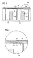
- each of the tuning structures 34a, 34b is provided with a metal plating on both sides of the base member 30, such that each tuning structure 34a, 34b includes two metallic surfaces 42, 42' facing the resonators 16a, 16b and the respective cavity 12a, 12b and two metallic surfaces 44, 44' facing the top wall 24 ( Fig. 3 ) of the respective cavities 12a, 12b.
- the latter surfaces 44, 44' shall be referred to as "second metallic surfaces" here and in the following.
- the conductive plating surrounds the edges of the plastic base member 30 and provides a conductive connection between the upper and lower metallized surfaces 42, 44 and 42', 44'.
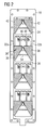
- Fig. 2 shows the lid 18 and the base member 30 of the tuning arrangement 28 as a whole as seen from inside the cavities 12a, 12b.
- the variable radio frequency band filter comprises four cavities and correspondingly four tuning structures of the type shown in Fig. 2 .
- the copper-plated parts of the tuning structures are marked with dashes.
- the lid 18 forming the top wall 24 of the cavities 12a, 12b is a simple silver-plated metal plate, such that the top wall 24 is flat.
- the base member 30 as a whole is a flat lattice structure stamped out of flat plastic material such that also the surfaces 42, 42', 44, 44' ( Fig. 1 , Fig. 3 ) are also perfectly flat.
- the base member 30 comprises one pair of stringers 32a, 32b, wherein the pair of stringers 32a, 32b is connected by bars 46 for stability reasons.
- the wing-shaped parts 36, 38 of the larger tuning structures 34 are stabilized by further bars 48 extending parallel to the stringers 32a, 32b.
- a small and uniform gap 50 is formed between the second metallic surface 44, 44' of the tuning structures 34a, 34b and the top wall 24 of the cavity 12a, 12b, the top wall 24 being formed by the lid 18.
- the width of the gap 50 is between 0,25 mm and 1 mm and the area of the parts 36a, 36b, 38a, 38b is between 0,25 cm 2 and 2 cm 2 , such that the capacitance of between 3pF and 15pF is formed between the second metallic surface 44, 44' and the top wall 24 of the cavity 12a, 12b.
- This capacitance is large enough to strongly couple the tuning structures 34a, 34b to the cavity wall 24 in the relevant frequency range between some 100 MHz and a few GHz, such that the tuning structures appear to be virtually grounded for the resonators 16a, 16b and for the microwaves generated by the resonator.
- the lower surfaces 42, 42' of the tuning structures effectively act as cavity walls, such that a movement of the tuning structures 34a, 34b has an effect which is identical to a variation of a shape of the respective cavity 12a, 12b.
- the tuning structures 34a, 34b are moved over the resonators 16a, 16b, the effect is identical to the effect of a reduction of the cavity height. Due to this virtual grounding, dielectric losses due to the tuning structures 34a, 34b can be almost completely avoided.
- a physical grounding of the tuning structures 34a, 34b which is complicated due to the fact that the tuning structures 34a, 34b are moveable, is avoided and replaced with a strong capacitive coupling.
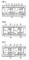
- Figs. 5 to 7 show a further embodiment of the invention, wherein the parts 36a, 36b, 38a, 38b of the tuning structures 34a, 34b are of roughly rectangular structure.
- Fig. 5 shows a first position of the tuning arrangement 28 corresponding to a high-frequency setting
- Fig. 6 shows a second position of the tuning arrangement 28 corresponding to a medium-frequency setting
- Fig. 7 shows a third position of the tuning arrangement 28 corresponding to a low-frequency setting.
- variable radio frequency band filter may comprise a linear actuator for moving the tuning arrangement 28, such that the frequency may be controlled by software.
- the parts of the base member 30 interconnecting the tuning structures 34a, 34b and the bars 46, 48 stabilizing the tuning arrangement 28 are void of metal plating, such that unwanted reflections of the electromagnetic waves may be avoided.
- conductive field blocking elements 52a, 52b are disposed on the top wall 24 of the cavities 12a, 12b in the vicinity of the parts of the plastic base member 30 being void of the metal plating.
- the field blocking elements 52a, 52b are attached to fixing structures 54 in the form of slits provided in the lid 18 ( Fig. 2 ).
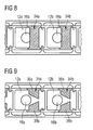
- Figs. 8 and 9 show further embodiments of the invention, wherein the tuning structures 34a, 34b are differently shaped.
- the tuning structures 34a, 34b are roughly bar-shaped and in Fig. 9 , the edges of the parts 36a, 36b, 38a, 38b facing the resonators 16a, 16b are formed as straight lines.
- the tuning arrangement including the tuning structures may be placed near the side walls of the cavities in a lateral direction with regard to the symmetry axis of the resonator. According to this embodiment, a very flat tunable radio frequency band filter may be achieved.
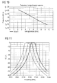
- Fig. 10 shows a curve representing the resonance frequency versus the position of the tuning arrangement, which can be continuously shifted in the longitudinal direction.
- the linearity of the tuning arrangement has been found to be very good over a very wide tuning range.
- the linearity may be achieved and/or enhanced by choosing a suitable shape for the tuning structures, which may e.g. be found using finite elements simulations.
- Fig. 11 shows the frequency spectrum of the resonators for the different positions in Figs. 5 to 7 .
- the leftmost and dotted curve corresponds to the low frequency configuration in Fig. 2
- the dashed curve corresponds to the medium frequency position in Fig. 6
- the rightmost curve corresponds to the high frequency situation in Fig. 5 .
Landscapes
- Physics & Mathematics (AREA)
- Electromagnetism (AREA)
- Control Of Motors That Do Not Use Commutators (AREA)
Priority Applications (3)
| Application Number | Priority Date | Filing Date | Title |
|---|---|---|---|
| EP08004027.2A EP2099091B1 (fr) | 2008-03-04 | 2008-03-04 | Filtre de bande de fréquence radio variable |
| CN200910134654.2A CN101645526B (zh) | 2008-03-04 | 2009-03-04 | 可变射频带通滤波器 |
| US12/379,936 US7969260B2 (en) | 2008-03-04 | 2009-03-04 | Variable radio frequency band filter |
Applications Claiming Priority (1)
| Application Number | Priority Date | Filing Date | Title |
|---|---|---|---|
| EP08004027.2A EP2099091B1 (fr) | 2008-03-04 | 2008-03-04 | Filtre de bande de fréquence radio variable |
Publications (2)
| Publication Number | Publication Date |
|---|---|
| EP2099091A1 true EP2099091A1 (fr) | 2009-09-09 |
| EP2099091B1 EP2099091B1 (fr) | 2017-11-22 |
Family
ID=39446008
Family Applications (1)
| Application Number | Title | Priority Date | Filing Date |
|---|---|---|---|
| EP08004027.2A Active EP2099091B1 (fr) | 2008-03-04 | 2008-03-04 | Filtre de bande de fréquence radio variable |
Country Status (3)
| Country | Link |
|---|---|
| US (1) | US7969260B2 (fr) |
| EP (1) | EP2099091B1 (fr) |
| CN (1) | CN101645526B (fr) |
Cited By (1)
| Publication number | Priority date | Publication date | Assignee | Title |
|---|---|---|---|---|
| ITVR20110005A1 (it) * | 2011-01-14 | 2012-07-15 | Gianfranco Natali | Dispositivo per la sintonizzazione di filtri passa-banda per radiofrequenze e metodo per la sua realizzazione |
Families Citing this family (12)
| Publication number | Priority date | Publication date | Assignee | Title |
|---|---|---|---|---|
| CN102231453B (zh) * | 2009-11-13 | 2014-03-26 | 鸿富锦精密工业(深圳)有限公司 | 空腔滤波器 |
| CN201946721U (zh) * | 2010-12-27 | 2011-08-24 | 鸿富锦精密工业(深圳)有限公司 | 空腔滤波器 |
| WO2013129817A1 (fr) * | 2012-02-27 | 2013-09-06 | 주식회사 케이엠더블유 | Filtre de fréquence radio ayant une structure de cavité |
| KR101869757B1 (ko) | 2012-02-27 | 2018-06-21 | 주식회사 케이엠더블유 | 캐비티 구조를 가진 무선 주파수 필터 |
| JP6006079B2 (ja) * | 2012-10-23 | 2016-10-12 | Necエンジニアリング株式会社 | チューナブル帯域通過フィルタ |
| WO2015070450A1 (fr) | 2013-11-18 | 2015-05-21 | 华为技术有限公司 | Résonateur, filtre, duplexeur et multiplexeur |
| JP6097815B1 (ja) * | 2015-12-18 | 2017-03-15 | 古河電気工業株式会社 | 接着剤組成物、これを用いた被着体の接合方法および積層体の製造方法 |
| WO2017134246A1 (fr) * | 2016-02-05 | 2017-08-10 | Spinner Gmbh | Structures de filtre pour mesures d'intermodulation passive |
| CN107204503B (zh) * | 2016-03-18 | 2020-05-05 | 通玉科技有限公司 | Rf滤波器 |
| KR102919910B1 (ko) * | 2020-07-09 | 2026-01-29 | 삼성전자주식회사 | 무선 통신 시스템에서 안테나 필터 및 이를 포함하는 전자 장치 |
| EP4239786A1 (fr) | 2022-03-03 | 2023-09-06 | Nokia Solutions and Networks Oy | Filtre à fréquence réglable |
| CN115663434B (zh) * | 2022-12-29 | 2023-03-21 | 成都联帮微波通信工程有限公司 | 一种滤波器机构 |
Citations (4)
| Publication number | Priority date | Publication date | Assignee | Title |
|---|---|---|---|---|
| JPS62209901A (ja) * | 1986-03-11 | 1987-09-16 | Murata Mfg Co Ltd | マイクロ波発振器の周波数可変機構 |
| US20050040916A1 (en) * | 2003-08-23 | 2005-02-24 | Kmw Inc. | Variable radio frequency band filter |
| US20060139128A1 (en) * | 2003-03-18 | 2006-06-29 | Filtronic Comtek Oy | Resonator filter |
| EP1885018A1 (fr) * | 2006-07-24 | 2008-02-06 | Matsushita Electric Industrial Co., Ltd. | Filtre bandepassante accordable |
Family Cites Families (3)
| Publication number | Priority date | Publication date | Assignee | Title |
|---|---|---|---|---|
| FI113578B (fi) * | 1999-03-03 | 2004-05-14 | Filtronic Lk Oy | Resonaattorisuodatin |
| EP1164655B1 (fr) * | 2000-06-15 | 2010-03-17 | Panasonic Corporation | Résonateur et filtre haute fréquence |
| US20050219013A1 (en) * | 2004-04-06 | 2005-10-06 | Pavan Kumar | Comb-line filter |
-
2008
- 2008-03-04 EP EP08004027.2A patent/EP2099091B1/fr active Active
-
2009
- 2009-03-04 CN CN200910134654.2A patent/CN101645526B/zh active Active
- 2009-03-04 US US12/379,936 patent/US7969260B2/en active Active
Patent Citations (5)
| Publication number | Priority date | Publication date | Assignee | Title |
|---|---|---|---|---|
| JPS62209901A (ja) * | 1986-03-11 | 1987-09-16 | Murata Mfg Co Ltd | マイクロ波発振器の周波数可変機構 |
| US20060139128A1 (en) * | 2003-03-18 | 2006-06-29 | Filtronic Comtek Oy | Resonator filter |
| US20050040916A1 (en) * | 2003-08-23 | 2005-02-24 | Kmw Inc. | Variable radio frequency band filter |
| US7205868B2 (en) | 2003-08-23 | 2007-04-17 | Kmw, Inc. | Variable radio frequency band filter |
| EP1885018A1 (fr) * | 2006-07-24 | 2008-02-06 | Matsushita Electric Industrial Co., Ltd. | Filtre bandepassante accordable |
Cited By (1)
| Publication number | Priority date | Publication date | Assignee | Title |
|---|---|---|---|---|
| ITVR20110005A1 (it) * | 2011-01-14 | 2012-07-15 | Gianfranco Natali | Dispositivo per la sintonizzazione di filtri passa-banda per radiofrequenze e metodo per la sua realizzazione |
Also Published As
| Publication number | Publication date |
|---|---|
| US7969260B2 (en) | 2011-06-28 |
| CN101645526A (zh) | 2010-02-10 |
| US20090237185A1 (en) | 2009-09-24 |
| EP2099091B1 (fr) | 2017-11-22 |
| CN101645526B (zh) | 2014-02-26 |
Similar Documents
| Publication | Publication Date | Title |
|---|---|---|
| EP2099091B1 (fr) | Filtre de bande de fréquence radio variable | |
| CN107359394B (zh) | 可调电磁混合耦合滤波器 | |
| US20150244050A1 (en) | Rf filter for adjusting coupling amount or transmission zero | |
| EP1174944A2 (fr) | Filtre passe-bande accordable | |
| CN107425247B (zh) | 多谐振器非相邻耦合 | |
| US8847709B2 (en) | Resonator filter | |
| EP3146589B1 (fr) | Élément de syntonisation pour résonateur à radiofréquence | |
| CN116417770B (zh) | 滤波器、容性耦合结构及其调节方法 | |
| EP1034576B1 (fr) | Resonateur coaxial multisurface couple | |
| US6396366B1 (en) | Coaxial cavity resonator | |
| EP1962369B1 (fr) | Résonateur multimodal diélectrique | |
| KR101754278B1 (ko) | Tem모드 유전체 도파관 공진기 및 이를 이용한 유전체 도파관 필터 | |
| US11139547B2 (en) | Tunable bandpass filter and method of forming the same | |
| EP2624361B1 (fr) | Résonateur coaxial et son emploi avec un filtre diélectrique, un module de communication sans fil et un dispositif de communication sans fil | |
| JP6720742B2 (ja) | 誘電体導波管型共振部品およびその特性調整方法 | |
| EP3598568B1 (fr) | Sonde réglable pour filtres rf interconnectés hautes performances | |
| CN117276830A (zh) | 基于混合电磁耦合及曲线谐振器的小型化腔体滤波器 | |
| US7796000B2 (en) | Filter coupled by conductive plates having curved surface | |
| Chen et al. | Metal-dielectric coaxial dual-mode resonator for compact inline bandpass filters | |
| CN112768861A (zh) | 用于滤波器的耦合结构、滤波器及射频器件 | |
| JP2021078048A (ja) | 誘電体共振部品 | |
| KR102873802B1 (ko) | 무선통신 시스템 필터 | |
| JP5077305B2 (ja) | 高周波フィルタ | |
| Xu et al. | A Bandwidth Enhanced Dielectric Filter for Ka-band High-throughput Satellite | |
| Hung et al. | Fully reconfigurable evanescent mode bandpass filter embedded with metallic grid |
Legal Events
| Date | Code | Title | Description |
|---|---|---|---|
| PUAI | Public reference made under article 153(3) epc to a published international application that has entered the european phase |
Free format text: ORIGINAL CODE: 0009012 |
|
| AK | Designated contracting states |
Kind code of ref document: A1 Designated state(s): AT BE BG CH CY CZ DE DK EE ES FI FR GB GR HR HU IE IS IT LI LT LU LV MC MT NL NO PL PT RO SE SI SK TR |
|
| AX | Request for extension of the european patent |
Extension state: AL BA MK RS |
|
| 17P | Request for examination filed |
Effective date: 20100309 |
|
| 17Q | First examination report despatched |
Effective date: 20100331 |
|
| AKX | Designation fees paid |
Designated state(s): AT BE BG CH CY CZ DE DK EE ES FI FR GB GR HR HU IE IS IT LI LT LU LV MC MT NL NO PL PT RO SE SI SK TR |
|
| RAP1 | Party data changed (applicant data changed or rights of an application transferred) |
Owner name: NOKIA SOLUTIONS AND NETWORKS OY |
|
| GRAP | Despatch of communication of intention to grant a patent |
Free format text: ORIGINAL CODE: EPIDOSNIGR1 |
|
| INTG | Intention to grant announced |
Effective date: 20170616 |
|
| RAP1 | Party data changed (applicant data changed or rights of an application transferred) |
Owner name: HMD GLOBAL OY |
|
| GRAS | Grant fee paid |
Free format text: ORIGINAL CODE: EPIDOSNIGR3 |
|
| GRAA | (expected) grant |
Free format text: ORIGINAL CODE: 0009210 |
|
| AK | Designated contracting states |
Kind code of ref document: B1 Designated state(s): AT BE BG CH CY CZ DE DK EE ES FI FR GB GR HR HU IE IS IT LI LT LU LV MC MT NL NO PL PT RO SE SI SK TR |
|
| REG | Reference to a national code |
Ref country code: GB Ref legal event code: FG4D |
|
| REG | Reference to a national code |
Ref country code: CH Ref legal event code: EP |
|
| REG | Reference to a national code |
Ref country code: IE Ref legal event code: FG4D |
|
| REG | Reference to a national code |
Ref country code: AT Ref legal event code: REF Ref document number: 949210 Country of ref document: AT Kind code of ref document: T Effective date: 20171215 |
|
| REG | Reference to a national code |
Ref country code: DE Ref legal event code: R096 Ref document number: 602008053024 Country of ref document: DE |
|
| REG | Reference to a national code |
Ref country code: NL Ref legal event code: MP Effective date: 20171122 |
|
| REG | Reference to a national code |
Ref country code: LT Ref legal event code: MG4D |
|
| REG | Reference to a national code |
Ref country code: AT Ref legal event code: MK05 Ref document number: 949210 Country of ref document: AT Kind code of ref document: T Effective date: 20171122 |
|
| PG25 | Lapsed in a contracting state [announced via postgrant information from national office to epo] |
Ref country code: LT Free format text: LAPSE BECAUSE OF FAILURE TO SUBMIT A TRANSLATION OF THE DESCRIPTION OR TO PAY THE FEE WITHIN THE PRESCRIBED TIME-LIMIT Effective date: 20171122 Ref country code: ES Free format text: LAPSE BECAUSE OF FAILURE TO SUBMIT A TRANSLATION OF THE DESCRIPTION OR TO PAY THE FEE WITHIN THE PRESCRIBED TIME-LIMIT Effective date: 20171122 Ref country code: NO Free format text: LAPSE BECAUSE OF FAILURE TO SUBMIT A TRANSLATION OF THE DESCRIPTION OR TO PAY THE FEE WITHIN THE PRESCRIBED TIME-LIMIT Effective date: 20180222 Ref country code: FI Free format text: LAPSE BECAUSE OF FAILURE TO SUBMIT A TRANSLATION OF THE DESCRIPTION OR TO PAY THE FEE WITHIN THE PRESCRIBED TIME-LIMIT Effective date: 20171122 Ref country code: NL Free format text: LAPSE BECAUSE OF FAILURE TO SUBMIT A TRANSLATION OF THE DESCRIPTION OR TO PAY THE FEE WITHIN THE PRESCRIBED TIME-LIMIT Effective date: 20171122 Ref country code: SE Free format text: LAPSE BECAUSE OF FAILURE TO SUBMIT A TRANSLATION OF THE DESCRIPTION OR TO PAY THE FEE WITHIN THE PRESCRIBED TIME-LIMIT Effective date: 20171122 |
|
| PG25 | Lapsed in a contracting state [announced via postgrant information from national office to epo] |
Ref country code: AT Free format text: LAPSE BECAUSE OF FAILURE TO SUBMIT A TRANSLATION OF THE DESCRIPTION OR TO PAY THE FEE WITHIN THE PRESCRIBED TIME-LIMIT Effective date: 20171122 Ref country code: LV Free format text: LAPSE BECAUSE OF FAILURE TO SUBMIT A TRANSLATION OF THE DESCRIPTION OR TO PAY THE FEE WITHIN THE PRESCRIBED TIME-LIMIT Effective date: 20171122 Ref country code: GR Free format text: LAPSE BECAUSE OF FAILURE TO SUBMIT A TRANSLATION OF THE DESCRIPTION OR TO PAY THE FEE WITHIN THE PRESCRIBED TIME-LIMIT Effective date: 20180223 Ref country code: HR Free format text: LAPSE BECAUSE OF FAILURE TO SUBMIT A TRANSLATION OF THE DESCRIPTION OR TO PAY THE FEE WITHIN THE PRESCRIBED TIME-LIMIT Effective date: 20171122 Ref country code: BG Free format text: LAPSE BECAUSE OF FAILURE TO SUBMIT A TRANSLATION OF THE DESCRIPTION OR TO PAY THE FEE WITHIN THE PRESCRIBED TIME-LIMIT Effective date: 20180222 |
|
| PG25 | Lapsed in a contracting state [announced via postgrant information from national office to epo] |
Ref country code: DK Free format text: LAPSE BECAUSE OF FAILURE TO SUBMIT A TRANSLATION OF THE DESCRIPTION OR TO PAY THE FEE WITHIN THE PRESCRIBED TIME-LIMIT Effective date: 20171122 Ref country code: EE Free format text: LAPSE BECAUSE OF FAILURE TO SUBMIT A TRANSLATION OF THE DESCRIPTION OR TO PAY THE FEE WITHIN THE PRESCRIBED TIME-LIMIT Effective date: 20171122 Ref country code: CY Free format text: LAPSE BECAUSE OF FAILURE TO SUBMIT A TRANSLATION OF THE DESCRIPTION OR TO PAY THE FEE WITHIN THE PRESCRIBED TIME-LIMIT Effective date: 20171122 Ref country code: CZ Free format text: LAPSE BECAUSE OF FAILURE TO SUBMIT A TRANSLATION OF THE DESCRIPTION OR TO PAY THE FEE WITHIN THE PRESCRIBED TIME-LIMIT Effective date: 20171122 Ref country code: SK Free format text: LAPSE BECAUSE OF FAILURE TO SUBMIT A TRANSLATION OF THE DESCRIPTION OR TO PAY THE FEE WITHIN THE PRESCRIBED TIME-LIMIT Effective date: 20171122 |
|
| REG | Reference to a national code |
Ref country code: DE Ref legal event code: R097 Ref document number: 602008053024 Country of ref document: DE |
|
| PG25 | Lapsed in a contracting state [announced via postgrant information from national office to epo] |
Ref country code: PL Free format text: LAPSE BECAUSE OF FAILURE TO SUBMIT A TRANSLATION OF THE DESCRIPTION OR TO PAY THE FEE WITHIN THE PRESCRIBED TIME-LIMIT Effective date: 20171122 Ref country code: IT Free format text: LAPSE BECAUSE OF FAILURE TO SUBMIT A TRANSLATION OF THE DESCRIPTION OR TO PAY THE FEE WITHIN THE PRESCRIBED TIME-LIMIT Effective date: 20171122 Ref country code: RO Free format text: LAPSE BECAUSE OF FAILURE TO SUBMIT A TRANSLATION OF THE DESCRIPTION OR TO PAY THE FEE WITHIN THE PRESCRIBED TIME-LIMIT Effective date: 20171122 |
|
| PLBE | No opposition filed within time limit |
Free format text: ORIGINAL CODE: 0009261 |
|
| STAA | Information on the status of an ep patent application or granted ep patent |
Free format text: STATUS: NO OPPOSITION FILED WITHIN TIME LIMIT |
|
| 26N | No opposition filed |
Effective date: 20180823 |
|
| REG | Reference to a national code |
Ref country code: CH Ref legal event code: PL |
|
| GBPC | Gb: european patent ceased through non-payment of renewal fee |
Effective date: 20180304 |
|
| PG25 | Lapsed in a contracting state [announced via postgrant information from national office to epo] |
Ref country code: SI Free format text: LAPSE BECAUSE OF FAILURE TO SUBMIT A TRANSLATION OF THE DESCRIPTION OR TO PAY THE FEE WITHIN THE PRESCRIBED TIME-LIMIT Effective date: 20171122 Ref country code: MC Free format text: LAPSE BECAUSE OF FAILURE TO SUBMIT A TRANSLATION OF THE DESCRIPTION OR TO PAY THE FEE WITHIN THE PRESCRIBED TIME-LIMIT Effective date: 20171122 |
|
| REG | Reference to a national code |
Ref country code: BE Ref legal event code: MM Effective date: 20180331 |
|
| REG | Reference to a national code |
Ref country code: IE Ref legal event code: MM4A |
|
| PG25 | Lapsed in a contracting state [announced via postgrant information from national office to epo] |
Ref country code: LU Free format text: LAPSE BECAUSE OF NON-PAYMENT OF DUE FEES Effective date: 20180304 |
|
| PG25 | Lapsed in a contracting state [announced via postgrant information from national office to epo] |
Ref country code: IE Free format text: LAPSE BECAUSE OF NON-PAYMENT OF DUE FEES Effective date: 20180304 |
|
| PG25 | Lapsed in a contracting state [announced via postgrant information from national office to epo] |
Ref country code: GB Free format text: LAPSE BECAUSE OF NON-PAYMENT OF DUE FEES Effective date: 20180304 Ref country code: CH Free format text: LAPSE BECAUSE OF NON-PAYMENT OF DUE FEES Effective date: 20180331 Ref country code: BE Free format text: LAPSE BECAUSE OF NON-PAYMENT OF DUE FEES Effective date: 20180331 Ref country code: LI Free format text: LAPSE BECAUSE OF NON-PAYMENT OF DUE FEES Effective date: 20180331 |
|
| PG25 | Lapsed in a contracting state [announced via postgrant information from national office to epo] |
Ref country code: FR Free format text: LAPSE BECAUSE OF NON-PAYMENT OF DUE FEES Effective date: 20180331 |
|
| PG25 | Lapsed in a contracting state [announced via postgrant information from national office to epo] |
Ref country code: MT Free format text: LAPSE BECAUSE OF NON-PAYMENT OF DUE FEES Effective date: 20180304 |
|
| PG25 | Lapsed in a contracting state [announced via postgrant information from national office to epo] |
Ref country code: TR Free format text: LAPSE BECAUSE OF FAILURE TO SUBMIT A TRANSLATION OF THE DESCRIPTION OR TO PAY THE FEE WITHIN THE PRESCRIBED TIME-LIMIT Effective date: 20171122 |
|
| PG25 | Lapsed in a contracting state [announced via postgrant information from national office to epo] |
Ref country code: PT Free format text: LAPSE BECAUSE OF FAILURE TO SUBMIT A TRANSLATION OF THE DESCRIPTION OR TO PAY THE FEE WITHIN THE PRESCRIBED TIME-LIMIT Effective date: 20171122 Ref country code: HU Free format text: LAPSE BECAUSE OF FAILURE TO SUBMIT A TRANSLATION OF THE DESCRIPTION OR TO PAY THE FEE WITHIN THE PRESCRIBED TIME-LIMIT; INVALID AB INITIO Effective date: 20080304 |
|
| PG25 | Lapsed in a contracting state [announced via postgrant information from national office to epo] |
Ref country code: IS Free format text: LAPSE BECAUSE OF FAILURE TO SUBMIT A TRANSLATION OF THE DESCRIPTION OR TO PAY THE FEE WITHIN THE PRESCRIBED TIME-LIMIT Effective date: 20180322 |
|
| PGFP | Annual fee paid to national office [announced via postgrant information from national office to epo] |
Ref country code: DE Payment date: 20260319 Year of fee payment: 19 |