EP2099159A1 - Surveillance efficace des signaux d'entrée/sortie de matériel - Google Patents
Surveillance efficace des signaux d'entrée/sortie de matériel Download PDFInfo
- Publication number
- EP2099159A1 EP2099159A1 EP08172957A EP08172957A EP2099159A1 EP 2099159 A1 EP2099159 A1 EP 2099159A1 EP 08172957 A EP08172957 A EP 08172957A EP 08172957 A EP08172957 A EP 08172957A EP 2099159 A1 EP2099159 A1 EP 2099159A1
- Authority
- EP
- European Patent Office
- Prior art keywords
- ports
- hardware
- circuit
- communication device
- command
- Prior art date
- Legal status (The legal status is an assumption and is not a legal conclusion. Google has not performed a legal analysis and makes no representation as to the accuracy of the status listed.)
- Withdrawn
Links
- 238000012544 monitoring process Methods 0.000 title description 2
- 238000004891 communication Methods 0.000 abstract description 44
- 230000006855 networking Effects 0.000 description 15
- 238000000034 method Methods 0.000 description 13
- RYGMFSIKBFXOCR-UHFFFAOYSA-N Copper Chemical compound [Cu] RYGMFSIKBFXOCR-UHFFFAOYSA-N 0.000 description 5
- 229910052802 copper Inorganic materials 0.000 description 5
- 239000010949 copper Substances 0.000 description 5
- 238000010586 diagram Methods 0.000 description 5
- 230000003287 optical effect Effects 0.000 description 4
- 239000002699 waste material Substances 0.000 description 4
- 230000008878 coupling Effects 0.000 description 2
- 238000010168 coupling process Methods 0.000 description 2
- 238000005859 coupling reaction Methods 0.000 description 2
- 238000013461 design Methods 0.000 description 2
- 239000000835 fiber Substances 0.000 description 2
- 239000013307 optical fiber Substances 0.000 description 2
- 238000012546 transfer Methods 0.000 description 2
- 230000002411 adverse Effects 0.000 description 1
- 238000003491 array Methods 0.000 description 1
- 238000004590 computer program Methods 0.000 description 1
- 238000013500 data storage Methods 0.000 description 1
- 238000011161 development Methods 0.000 description 1
- 230000006870 function Effects 0.000 description 1
- 238000004519 manufacturing process Methods 0.000 description 1
- 230000007246 mechanism Effects 0.000 description 1
- 238000012986 modification Methods 0.000 description 1
- 230000004048 modification Effects 0.000 description 1
- 230000008520 organization Effects 0.000 description 1
- 230000008569 process Effects 0.000 description 1
- 238000012545 processing Methods 0.000 description 1
- 230000009467 reduction Effects 0.000 description 1
- 239000004065 semiconductor Substances 0.000 description 1
Images


Classifications
-
- H—ELECTRICITY
- H04—ELECTRIC COMMUNICATION TECHNIQUE
- H04L—TRANSMISSION OF DIGITAL INFORMATION, e.g. TELEGRAPHIC COMMUNICATION
- H04L1/00—Arrangements for detecting or preventing errors in the information received
- H04L1/22—Arrangements for detecting or preventing errors in the information received using redundant apparatus to increase reliability
Definitions
- one set of hardware called the command hardware or "COM”
- another independent set of hardware called the monitor hardware or "MON”
- a wrap-back mechanism couples the transmitter of the COM hardware to a receiver in the MON hardware.
- each received signal is delivered to two independent receivers: one in the monitor hardware and one in the command hardware.
- such systems require three receivers and one transmitter: one transmitter and one receiver in the command hardware and two receivers in the monitor hardware.
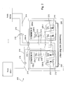
- FIG. 1 illustrates the physical layer portion of a COM/MON system that is implemented using the similar hardware for both the command and monitor hardware.
- a device 100 comprises two ports 105.
- the device 100 is implemented using two transceiver circuits, one of which (also referred to here as the "COM IC" 104) is used to implement the command hardware for each port 105 and the other of which (also referred to here as the "MON IC" 106) is used to implement the monitor hardware for each port 105.
- Each of the circuits 104 and 106 includes four transceivers 108, each of which includes a respective transmitter 110 and a respective receiver 112.
- the one transmitter and one receiver needed to implement the COM portion for each port 105 are implemented using a single one of the transceivers 108 in the COM IC 104.
- the transmitter 110 and receiver 112 used to implement the COM portion for each port 105 are coupled to the transmit portion 114 and receive portion 116 portion, respectively, of the communication channel 118 to which that port 105 is coupled.
- the two receivers needed to implement the MON portion for each port 105 are implemented using the receivers 112 of two of the transceivers 108 included in the MON IC 106.
- One of the receivers 112 is coupled to the transmitter 110 for the respective COM portion for that port 105 using a wrap-back link 120, and the other receiver 112 is coupled to the receive portion 116 of the communication channel 118 in order to receive data from the communication channel 118.
- FIG. 1 uses similar hardware to implement the physical layer for each of the COM and MON portions for each port 105. However, as shown in FIG. 1 , for each port 105 of the device 100, one entire transceiver 108 in the COM IC 104 and two transmitters 110 in the MON IC 106 are wasted (where the wasted elements are marked with an "X").
- a communication device comprises first and second circuits to implement a plurality of ports via which the communicative device is operable to communicate over a plurality of communication channels.
- the communication device comprises: command hardware that includes a first transmitter to transmit data over a respective one of the plurality of channels and a first receiver to receive data from the respective one of the plurality of channels; and monitor hardware that includes a second receiver coupled to the first transmitter and a third receiver coupled to the respective one of the plurality of channels.
- the first circuit comprises the command hardware for a first subset of the plurality of ports.
- the second circuit comprises the monitor hardware for the first subset of the plurality of ports and the command hardware for a second subset of the plurality of ports.
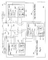
- FIG. 2 is a block diagram of one embodiment of a network 201 that comprises a fault-tolerant networking communication device 200.
- the device 200 is implemented as a networking device 200 that interconnects a plurality of nodes 203 (individually labeled as 203-1, ..., 203-N in FIG. 2 ).
- the networking device 200 comprises at least one port 205 for each node 203 that couples the node 203 to the networking device 200 via a respective communication channel 218.
- the ports 205 are individually labeled as 205-1, ..., 205-N in FIG. 2 .
- the networking device 200 is implemented as an Open Systems Interconnection (OSI) International Standards Organization (ISO) layer-1/layer-2 networking device (such as a hub or repeater) in which any data validly received on one port 205 of the networking device 200 is broadcast on the other ports of the networking device 200.
- OSI Open Systems Interconnection
- ISO International Standards Organization
- the networking device is implemented as an OSI ISO layer 3 networking device such as a bridge, switch, or router, in which any data validly received on one port of the networking device 200 is re-transmitted on one or more of the other ports of the networking device 200.
- the networking device 200 implements various mixes of protocol layering and functionality, and can include functionality not conforming to standard communication models.
- the network 201 comprises a local area network used in or with a satellite or other vehicle (such as an automobile, aircraft, and/or space craft), where the nodes 203-1 ... 203-N are implemented as sensors, processing units, memory devices, etc. associated with the operation of such a vehicle.
- a satellite or other vehicle such as an automobile, aircraft, and/or space craft
- the nodes 203-1 ... 203-N are implemented as sensors, processing units, memory devices, etc. associated with the operation of such a vehicle.
- Other embodiments are implemented in other ways and for other applications.
- Device 200 includes circuit 204-1 and circuit 204-2.
- device 200 includes a respective command module 224 (also referred to herein as “COM” or “command” hardware and individually labeled 224-1, ..., 224-N) and a monitor module 226 (also referred to herein as "MON” or “monitor” hardware and individually labeled 226-1, ..., 226-N).
- Each command module 224 comprises a transceiver having a transmitter 210 and a receiver 212.
- Each monitor module 226 comprises two transceivers, each of which including a respective transmitter 210 and a receiver 212. Unlike the device 100 shown in FIG.
- both command modules 224 and monitor modules 226 are located in each of circuits 204-1 and 204-2.
- the respective command module 224 is located in one of the circuits 204-1 or 204-2 while the corresponding monitor module 226 is located in the other circuit 204-2 or 204-1.
- that command module 224 is monitored by a corresponding monitor module 226 in circuit 204-2.
- that command module 224 is monitored by a corresponding monitor module 226 in circuit 204-1.
- the transmitter 210 in that port's command module 224 is coupled to the transmit portion 214 of the communication channel 218 to which that port 205 is coupled.
- the receiver 212 in that port's command module 224 is coupled to the receive portion 216 of the communication channel 218 to which that port 205 is coupled.
- Each port's monitor module 226 has two receivers 212: one coupled to the transmitter 210 of the corresponding command module 224 and another coupled to the receive portion 216 of the communication channel 218 to which that port is coupled.
- Each communication channel is implemented using a suitable communication medium or media (for example, metallic communication media such as twisted pair cables, coaxial cable and optical communication media such as fiber optic cables).
- each communication channel also uses suitably partitioned (for example, via code, frequency, space, or time multiplexing) radio frequency (RF) or free-space optical paths.
- the transmit portion 214 of each communication channel 218 is the communication medium or media over which data is transmitted.
- the receive portion 216 of each communication channel 218 is the communication medium or media from which data is received.
- the transmit portion 214 and the receive portion 216 of the communication channel 218 is implemented using a separate communication medium or media.
- the communication channel 218 is implemented using a copper twisted-pair cable such as a category 5 (“CAT 5") cable
- CAT 5 category 5
- the former pair of copper wires comprises the transmit portion 214 of the communication channel 218, and the latter pair of copper wires comprises the receive portion 216 of the communication channel 218.
- the communication channel 218 is implemented using fiber optic cables, one optical cable is used to transmit data for that communication channel 218 and another optical cable is used to receive data from that communication channel 218.
- the first optical fiber comprises the transmit portion 214 of the communication channel 218 and the second optical fiber comprises the receive portion 216 of the communication channel 218.
- the transmit portion 214 and the receive portion 216 of the communication channel 218 are implemented using the same communication medium or media, for example, by using a multiplexing technique such as time division multiplexing, frequency division multiplexing, wave division multiplexing, or code division multiplexing.
- each transmit portion and each receive portion of a communication channel uses multiple segments of media in parallel.
- circuit 204-1 it is necessary for the circuit 204-1 to communicate with circuit 204-2.
- communication between circuits 204-1 and 204-2 is necessary in some embodiments to transfer data received on port 205-1 by circuit 204-1 to circuit 204-2 for transmitting on port 205-N.
- Exemplary situations in which communication between circuits 204 is necessary or desired include embodiments comprising three or more circuits 204 or embodiments wherein each transmitter can have only one receiver (such as for quantum cryptography ports 205 with the quantum devices embedded in each circuit 204).
- an inter-chip link 234 is used to facilitate the necessary communication between circuits 204-1 and 204-2.
- inter-chip link 234 is not necessary in some embodiments since each of circuits 204-1 and 204-2 receive a copy of all inputs on ports 205-1 ... 205-N.
- a circuit having a monitor module 226 is precluded from providing information via the inter-chip link 234 which influences the output of the command module 224 being monitored.
- a circuit having a command module 224 is precluded from providing information via the inter-chip link 234 which adversely impacts the ability of the corresponding monitor module 226 to monitor the command module 224.
- FIG. 2 an embodiment is shown in which the COM/MON techniques described here are used to implement a networking device, it is to be understood that such techniques can be used in other embodiments.
- the COM/MON techniques described here can be used to implement terminal nodes.
- FIG. 3 One example of such an embodiment is shown in FIG. 3 .
- substantially the same COM/MON functionality described above in connection with the embodiment shown in FIG. 2 is used to implement the COM/MON functionality of terminal node 300 (and the same reference numerals are used in FIG. 3 as in FIG. 2 to refer to substantially similar functionality, the description of which is not repeated here for clarity).
- the terminal node 300 typically will have fewer ports 205.
- the terminal node 300 comprises two ports 205, each of which is coupled to a different networking device 302 via a respective communication channel 218.
- embodiments of the devices 200 and 300 reduce waste typically associated with conventional devices, such as device 100.
- the embodiments described in FIGS. 2 and 3 reduce the waste of a transceiver for each port. This reduction in waste enables lower production costs and/or the ability to provide support for more ports than a conventional device of similar size.
- the additional ports are a product of being able to use the transmitters and receivers wasted in conventional devices to provide additional ports.
- circuits 204-2 and 204-1 share identical designs, in some embodiments, which further reduces development and/or logistics costs.
- FIGs. 2 and 3 in which the COM/MON techniques described here are used in devices implemented with two circuits 204-1 and 204-2, it is to be understood that such techniques can be used in other embodiments.
- the COM/MON techniques described here can be used to implement devices having more than two circuits 204-1 and 204-2.
- FIG. 4 substantially the same COM/MON functionality described above in connection with the embodiment shown in FIG. 2 is used to implement the COM/MON functionality of device 400 (and the same reference numerals are used in FIG. 4 as in FIG. 2 to refer to substantially similar functionality, the description of which is not repeated here for clarity).
- device 400 includes three COM/MON circuits 204-1, 204-2, and 204-3.
- Circuits 204-1 ... 204-3 monitor one another as described above.
- command module 224-1 in circuit 204-1 is monitored by monitor module 226-1 in circuit 204-2.
- command module 224-2 in circuit 204-2 is monitored by monitor module 226-2 in circuit 204-3.
- command module 224-3 in circuit 204-3 is monitored by monitor module 226-3 in circuit 204-1.
- circuit 204-1 is coupled to circuit 204-3 via an inter-chip link 234 in order to facilitate communication between circuits 204-1 and 204-3 when necessary, e.g. to transfer data from port 205-2 to port 205-1, circuit 204-3 sends the data from port 205-2 to circuit 204-1 so that its command module 224-1 can transmit the data to port 205-1.
- circuit 204-3 is coupled to circuit 204-2 and circuit 204-1 is coupled to circuit 204-2 via an inter-chip link 234 to facilitate communication between circuits 204-1, 204-2 and 204-3.
- circuits 204-1 ... 204-3 are able to monitor and communicate with one another.
- the pattern of coupling circuits 204-1 ... 204-3 to monitor one another can be extended to include four or more circuits, each circuit monitoring another.
- each COM module 224 still has an associated MON module 226 in an independent circuit and each independent circuit contains a mix of COM and MON modules.
- the methods and techniques described here may be implemented in digital electronic circuitry, or with a programmable processor (for example, a special-purpose processor or a general-purpose processor such as a computer) firmware, software, or in combinations of them.
- Apparatus embodying these techniques may include appropriate input and output devices, a programmable processor, and a storage medium tangibly embodying program instructions for execution by the programmable processor.
- a process embodying these techniques may be performed by a programmable processor executing a program of instructions to perform desired functions by operating on input data and generating appropriate output.
- the techniques may advantageously be implemented in one or more programs that are executable on a programmable system including at least one programmable processor coupled to receive data and instructions from, and to transmit data and instructions to, a data storage system, at least one input device, and at least one output device.
- a processor will receive instructions and data from a read-only memory and/or a random access memory.
- Storage devices suitable for tangibly embodying computer program instructions and data include all forms of non-volatile memory, including by way of example semiconductor memory devices, such as EPROM, EEPROM, and flash memory devices; magnetic disks such as internal hard disks and removable disks; magnetooptical disks; and DVD disks. Any of the foregoing may be supplemented by, or incorporated in, specially-designed application-specific integrated circuits (ASICs), field programmable gate arrays (FPGAs), or other circuitry.
- ASICs application-specific integrated circuits
- FPGAs field programmable gate arrays
Landscapes
- Engineering & Computer Science (AREA)
- Computer Networks & Wireless Communication (AREA)
- Signal Processing (AREA)
- Small-Scale Networks (AREA)
- Data Exchanges In Wide-Area Networks (AREA)
- Maintenance And Management Of Digital Transmission (AREA)
Applications Claiming Priority (1)
| Application Number | Priority Date | Filing Date | Title |
|---|---|---|---|
| US12/044,808 US8243614B2 (en) | 2008-03-07 | 2008-03-07 | Hardware efficient monitoring of input/output signals |
Publications (1)
| Publication Number | Publication Date |
|---|---|
| EP2099159A1 true EP2099159A1 (fr) | 2009-09-09 |
Family
ID=40719495
Family Applications (1)
| Application Number | Title | Priority Date | Filing Date |
|---|---|---|---|
| EP08172957A Withdrawn EP2099159A1 (fr) | 2008-03-07 | 2008-12-27 | Surveillance efficace des signaux d'entrée/sortie de matériel |
Country Status (3)
| Country | Link |
|---|---|
| US (1) | US8243614B2 (fr) |
| EP (1) | EP2099159A1 (fr) |
| JP (1) | JP2009290858A (fr) |
Families Citing this family (2)
| Publication number | Priority date | Publication date | Assignee | Title |
|---|---|---|---|---|
| KR101253324B1 (ko) * | 2008-12-16 | 2013-04-12 | 한국전자통신연구원 | 양자화 암호 통신을 위한 광 숏 펄스 생성장치 및 방법 |
| US10760485B2 (en) * | 2018-02-02 | 2020-09-01 | General Electric Company | Virtualizing data for a vehicle control system |
Citations (4)
| Publication number | Priority date | Publication date | Assignee | Title |
|---|---|---|---|---|
| EP1180877A2 (fr) * | 2000-08-18 | 2002-02-20 | Broadcom Corporation | Procédé et dispositif pour filtrer des paquets basé sur des flux de paquet en utilisant des tables d'adresses |
| EP1338974A2 (fr) * | 2000-10-03 | 2003-08-27 | Altima Communications, Inc. | Méthode et dispositif de bus entre chips partagé pour des passages de message et d'accès mémoire |
| US7020076B1 (en) * | 1999-10-26 | 2006-03-28 | California Institute Of Technology | Fault-tolerant communication channel structures |
| US20060190642A1 (en) * | 2005-02-24 | 2006-08-24 | International Business Machines Corporation | Method and apparatus for testing, characterizing and monitoring a chip interface using a second data path |
Family Cites Families (14)
| Publication number | Priority date | Publication date | Assignee | Title |
|---|---|---|---|---|
| US4849657A (en) * | 1984-09-17 | 1989-07-18 | Honeywell Inc. | Fault tolerant integrated circuit design |
| IT1213344B (it) * | 1986-09-17 | 1989-12-20 | Honoywell Information Systems | Architettura di calcolatore a tolleranza di guasto. |
| US4965717A (en) * | 1988-12-09 | 1990-10-23 | Tandem Computers Incorporated | Multiple processor system having shared memory with private-write capability |
| US5157780A (en) * | 1990-06-12 | 1992-10-20 | Advanced Micro Devices, Inc. | Master-slave checking system |
| US5648972A (en) * | 1995-07-11 | 1997-07-15 | Exar Corporation | V.35 integrated circuit transceiver with diagnostics loopback |
| US5956370A (en) * | 1996-01-17 | 1999-09-21 | Lsi Logic Corporation | Wrap-back test system and method |
| US5787114A (en) * | 1996-01-17 | 1998-07-28 | Lsi Logic Corporation | Loop-back test system and method |
| US6161202A (en) * | 1997-02-18 | 2000-12-12 | Ee-Signals Gmbh & Co. Kg | Method for the monitoring of integrated circuits |
| GB9705436D0 (en) * | 1997-03-15 | 1997-04-30 | Sharp Kk | Fault tolerant circuit arrangements |
| US6088754A (en) * | 1997-12-31 | 2000-07-11 | Cisco Technology, Inc. | Generic serial interface with automatic reconfigurability |
| US7182296B2 (en) * | 2002-03-28 | 2007-02-27 | Honeywell International, Inc. | Methods and apparatus for error-tolerant wrap-back ACE monitor |
| US7263593B2 (en) * | 2002-11-25 | 2007-08-28 | Hitachi, Ltd. | Virtualization controller and data transfer control method |
| JP4870414B2 (ja) * | 2005-03-31 | 2012-02-08 | 株式会社リコー | データ処理システム、データ処理装置、データ処理方法及びプログラム |
| JP4768565B2 (ja) * | 2006-09-28 | 2011-09-07 | 富士通セミコンダクター株式会社 | インターフェース装置及びトポロジ構築方法 |
-
2008
- 2008-03-07 US US12/044,808 patent/US8243614B2/en active Active
- 2008-12-27 EP EP08172957A patent/EP2099159A1/fr not_active Withdrawn
-
2009
- 2009-01-07 JP JP2009001560A patent/JP2009290858A/ja not_active Withdrawn
Patent Citations (4)
| Publication number | Priority date | Publication date | Assignee | Title |
|---|---|---|---|---|
| US7020076B1 (en) * | 1999-10-26 | 2006-03-28 | California Institute Of Technology | Fault-tolerant communication channel structures |
| EP1180877A2 (fr) * | 2000-08-18 | 2002-02-20 | Broadcom Corporation | Procédé et dispositif pour filtrer des paquets basé sur des flux de paquet en utilisant des tables d'adresses |
| EP1338974A2 (fr) * | 2000-10-03 | 2003-08-27 | Altima Communications, Inc. | Méthode et dispositif de bus entre chips partagé pour des passages de message et d'accès mémoire |
| US20060190642A1 (en) * | 2005-02-24 | 2006-08-24 | International Business Machines Corporation | Method and apparatus for testing, characterizing and monitoring a chip interface using a second data path |
Also Published As
| Publication number | Publication date |
|---|---|
| US8243614B2 (en) | 2012-08-14 |
| US20090225673A1 (en) | 2009-09-10 |
| JP2009290858A (ja) | 2009-12-10 |
Similar Documents
| Publication | Publication Date | Title |
|---|---|---|
| EP2752044B1 (fr) | Configurer un système d'antennes distribuées | |
| US10983942B1 (en) | Multi-master hybrid bus apparatus | |
| US20110170619A1 (en) | High Speed Switch With Data Converter Physical Ports And Processing Unit | |
| CN108696425B (zh) | 用于发送数据的飞行器通信系统 | |
| EP1193888B1 (fr) | Architecture de tranche pour radio multifonction | |
| US8243614B2 (en) | Hardware efficient monitoring of input/output signals | |
| RU2171544C2 (ru) | Система обработки, преобразования и распределения сообщения в неподвижном абонентском узле в широкополосных системах множественного доступа с кодовым разделением каналов местной сети радиосвязи | |
| CN111726138B (zh) | 射频电路和电子设备 | |
| CN104660320B (zh) | 一种信号传输装置、系统及方法 | |
| CN120476576B (zh) | 一种报文的寻址方法、装置及可读存储介质 | |
| JP7317948B2 (ja) | 車両間通信を確立するためのシステムおよび方法 | |
| CN112217594B (zh) | 一种新前传网络的管理控制方法和设备 | |
| CN114448462B (zh) | 用于信号发射/接收的模块以及相应的通信设备 | |
| CN104639201B (zh) | 一种基站的射频前端以及基站 | |
| US7751566B2 (en) | Apparatus using a time division multiple access bus for providing multiple levels of security in a communications system | |
| CN103428905A (zh) | 远程信息通信系统及方法 | |
| EP1271866A2 (fr) | Emetteur-récepteur partagé et insensible aux défaillances, et système correspondant | |
| US8023893B2 (en) | Method and system for wireless communication among integrated circuits within an enclosure | |
| CN111953419B (zh) | 光模块 | |
| JP2008545328A (ja) | 改良されたポイントツーポイント通信システム | |
| CN116193609A (zh) | 一种旁链路配置方法、网络侧设备、终端及介质 | |
| CN109687917B (zh) | 一种有源阵列天线 | |
| JP4450509B2 (ja) | 送信信号を結合するクロス・フレーム送信のための方法および装置 | |
| JPS58172039A (ja) | 光伝送システム | |
| CN119543983A (zh) | 一种通信装置、微波通信设备及系统 |
Legal Events
| Date | Code | Title | Description |
|---|---|---|---|
| PUAI | Public reference made under article 153(3) epc to a published international application that has entered the european phase |
Free format text: ORIGINAL CODE: 0009012 |
|
| 17P | Request for examination filed |
Effective date: 20081227 |
|
| AK | Designated contracting states |
Kind code of ref document: A1 Designated state(s): AT BE BG CH CY CZ DE DK EE ES FI FR GB GR HR HU IE IS IT LI LT LU LV MC MT NL NO PL PT RO SE SI SK TR |
|
| AX | Request for extension of the european patent |
Extension state: AL BA MK RS |
|
| STAA | Information on the status of an ep patent application or granted ep patent |
Free format text: STATUS: THE APPLICATION HAS BEEN WITHDRAWN |
|
| 18W | Application withdrawn |
Effective date: 20091001 |