EP2101169A2 - Fluoreszenzerkennungsverfahren und Fluoreszenzerkennungsvorrichtung - Google Patents
Fluoreszenzerkennungsverfahren und Fluoreszenzerkennungsvorrichtung Download PDFInfo
- Publication number
- EP2101169A2 EP2101169A2 EP09003537A EP09003537A EP2101169A2 EP 2101169 A2 EP2101169 A2 EP 2101169A2 EP 09003537 A EP09003537 A EP 09003537A EP 09003537 A EP09003537 A EP 09003537A EP 2101169 A2 EP2101169 A2 EP 2101169A2
- Authority
- EP
- European Patent Office
- Prior art keywords
- intensity
- fluorescence
- electric field
- metal film
- detected
- Prior art date
- Legal status (The legal status is an assumption and is not a legal conclusion. Google has not performed a legal analysis and makes no representation as to the accuracy of the status listed.)
- Granted
Links
- 238000000034 method Methods 0.000 title claims description 22
- 230000005684 electric field Effects 0.000 claims abstract description 64
- 230000002708 enhancing effect Effects 0.000 claims abstract description 64
- 239000002184 metal Substances 0.000 claims abstract description 51
- 229910052751 metal Inorganic materials 0.000 claims abstract description 51
- 238000001514 detection method Methods 0.000 claims description 41
- 230000005284 excitation Effects 0.000 claims description 31
- 239000013076 target substance Substances 0.000 claims description 29
- 230000000694 effects Effects 0.000 claims description 5
- 230000001678 irradiating effect Effects 0.000 claims description 5
- 238000005259 measurement Methods 0.000 abstract description 19
- 238000001917 fluorescence detection Methods 0.000 abstract 1
- 239000000427 antigen Substances 0.000 description 16
- 102000036639 antigens Human genes 0.000 description 16
- 108091007433 antigens Proteins 0.000 description 16
- 230000003287 optical effect Effects 0.000 description 14
- 238000012937 correction Methods 0.000 description 7
- 239000004417 polycarbonate Substances 0.000 description 4
- 229920000515 polycarbonate Polymers 0.000 description 4
- 239000010931 gold Substances 0.000 description 3
- 239000007788 liquid Substances 0.000 description 3
- 239000000463 material Substances 0.000 description 3
- 238000006862 quantum yield reaction Methods 0.000 description 3
- 239000011347 resin Substances 0.000 description 3
- 229920005989 resin Polymers 0.000 description 3
- 238000010586 diagram Methods 0.000 description 2
- 230000002349 favourable effect Effects 0.000 description 2
- 229910052737 gold Inorganic materials 0.000 description 2
- 229920003229 poly(methyl methacrylate) Polymers 0.000 description 2
- 239000004926 polymethyl methacrylate Substances 0.000 description 2
- 230000035945 sensitivity Effects 0.000 description 2
- 238000010521 absorption reaction Methods 0.000 description 1
- 230000002411 adverse Effects 0.000 description 1
- 229910045601 alloy Inorganic materials 0.000 description 1
- 239000000956 alloy Substances 0.000 description 1
- 229960004407 chorionic gonadotrophin Drugs 0.000 description 1
- 229910052802 copper Inorganic materials 0.000 description 1
- 150000001925 cycloalkenes Chemical class 0.000 description 1
- 230000007613 environmental effect Effects 0.000 description 1
- MHMNJMPURVTYEJ-UHFFFAOYSA-N fluorescein-5-isothiocyanate Chemical compound O1C(=O)C2=CC(N=C=S)=CC=C2C21C1=CC=C(O)C=C1OC1=CC(O)=CC=C21 MHMNJMPURVTYEJ-UHFFFAOYSA-N 0.000 description 1
- 239000007850 fluorescent dye Substances 0.000 description 1
- 238000001215 fluorescent labelling Methods 0.000 description 1
- 238000005558 fluorometry Methods 0.000 description 1
- 239000011521 glass Substances 0.000 description 1
- PCHJSUWPFVWCPO-UHFFFAOYSA-N gold Chemical compound [Au] PCHJSUWPFVWCPO-UHFFFAOYSA-N 0.000 description 1
- 238000005286 illumination Methods 0.000 description 1
- 230000003993 interaction Effects 0.000 description 1
- 238000012544 monitoring process Methods 0.000 description 1
- 229910052759 nickel Inorganic materials 0.000 description 1
- 239000000049 pigment Substances 0.000 description 1
- 229910052697 platinum Inorganic materials 0.000 description 1
- 230000010287 polarization Effects 0.000 description 1
- 229920000098 polyolefin Polymers 0.000 description 1
- 230000001902 propagating effect Effects 0.000 description 1
- 102000004169 proteins and genes Human genes 0.000 description 1
- 108090000623 proteins and genes Proteins 0.000 description 1
- 238000011160 research Methods 0.000 description 1
- 229910052709 silver Inorganic materials 0.000 description 1
- 238000002198 surface plasmon resonance spectroscopy Methods 0.000 description 1
- 229910052719 titanium Inorganic materials 0.000 description 1
- 239000012780 transparent material Substances 0.000 description 1
- 238000007740 vapor deposition Methods 0.000 description 1
Images


Classifications
-
- G—PHYSICS
- G01—MEASURING; TESTING
- G01N—INVESTIGATING OR ANALYSING MATERIALS BY DETERMINING THEIR CHEMICAL OR PHYSICAL PROPERTIES
- G01N21/00—Investigating or analysing materials by the use of optical means, i.e. using sub-millimetre waves, infrared, visible or ultraviolet light
- G01N21/62—Systems in which the material investigated is excited whereby it emits light or causes a change in wavelength of the incident light
- G01N21/63—Systems in which the material investigated is excited whereby it emits light or causes a change in wavelength of the incident light optically excited
- G01N21/64—Fluorescence; Phosphorescence
- G01N21/645—Specially adapted constructive features of fluorimeters
- G01N21/648—Specially adapted constructive features of fluorimeters using evanescent coupling or surface plasmon coupling for the excitation of fluorescence
-
- G—PHYSICS
- G01—MEASURING; TESTING
- G01N—INVESTIGATING OR ANALYSING MATERIALS BY DETERMINING THEIR CHEMICAL OR PHYSICAL PROPERTIES
- G01N21/00—Investigating or analysing materials by the use of optical means, i.e. using sub-millimetre waves, infrared, visible or ultraviolet light
- G01N21/17—Systems in which incident light is modified in accordance with the properties of the material investigated
- G01N21/47—Scattering, i.e. diffuse reflection
-
- G—PHYSICS
- G01—MEASURING; TESTING
- G01N—INVESTIGATING OR ANALYSING MATERIALS BY DETERMINING THEIR CHEMICAL OR PHYSICAL PROPERTIES
- G01N21/00—Investigating or analysing materials by the use of optical means, i.e. using sub-millimetre waves, infrared, visible or ultraviolet light
- G01N21/62—Systems in which the material investigated is excited whereby it emits light or causes a change in wavelength of the incident light
- G01N21/63—Systems in which the material investigated is excited whereby it emits light or causes a change in wavelength of the incident light optically excited
- G01N21/64—Fluorescence; Phosphorescence
- G01N2021/6491—Measuring fluorescence and transmission; Correcting inner filter effect
- G01N2021/6493—Measuring fluorescence and transmission; Correcting inner filter effect by alternating fluorescence/transmission or fluorescence/reflection
-
- G—PHYSICS
- G01—MEASURING; TESTING
- G01N—INVESTIGATING OR ANALYSING MATERIALS BY DETERMINING THEIR CHEMICAL OR PHYSICAL PROPERTIES
- G01N21/00—Investigating or analysing materials by the use of optical means, i.e. using sub-millimetre waves, infrared, visible or ultraviolet light
- G01N21/17—Systems in which incident light is modified in accordance with the properties of the material investigated
- G01N21/25—Colour; Spectral properties, i.e. comparison of effect of material on the light at two or more different wavelengths or wavelength bands
- G01N21/27—Colour; Spectral properties, i.e. comparison of effect of material on the light at two or more different wavelengths or wavelength bands using photo-electric detection ; circuits for computing concentration
- G01N21/274—Calibration, base line adjustment, drift correction
Definitions
- a fluorescence detecting method that utilizes fluorescent labels (refer to Margarida M. L. M. Vareiro, et al., "Surface Plasmon Fluorescence Measurements of Human Chorionic Gonadotrophin: Role of Antibody Orientation in Obtaining Enhanced Sensitivity and Limit of Detection", Analytical Chemistry, Vol. 77, No. 8, pp. 2426-2431, 2005 .)
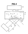
- the fluorescence detecting apparatus illustrated in Figure 3 is equipped with: a sensor chip 10 constituted by a dielectric plate 11 and a metal film 12 provided at a predetermined region on one surface of the dielectric plate; an excitation light outputting optical system 20 that outputs an excitation light beam L 0 at an incident angle that satisfies conditions for total reflection at the interface between the dielectric plate 11 and the metal film 12 from the side of the sensor chip 10 opposite the surface on which the metal film 12 is formed; and a photodetector 30 that detects fluorescence Lf generated by fluorescent labels F, which are attached to a detection target substance A, in the case that the detection target substance A having the fluorescent labels F attached thereto are present in a sample S in contact with the metal film 12.
- margins of error in the shapes and settings of sensor chips include shifting in the incident angle of excitation light beams caused by human error such as margins of errors in sensing and margins of error in setup of the optical system; and shifting in surface plasmon generating conditions due to physical factors such as the refractive indices of samples, the refractive indices of the sensor chips, irregularities on the surfaces of the sensor chips, the thicknesses of the metal films, and the densities of the metal films.
- changes in environmental temperatures during measurement may also lead to shifting in the aforementioned conditions, and therefore must be considered as well.
- the phrase "detecting the amount of a detection target substance” refers not only to detecting quantitative amounts of the detection target substance, but qualitatively detecting whether the detection target substance is present. The phrase also refers to detection of degrees of activity of the detection target substance.
- the intensity of fluorescence detected in each measurement is corrected based on the intensity of light which is scattered by the electric field enhancing field generated by irradiation of the excitation light.
- the intensity of fluorescence and the intensity of scattered light are both dependant on the generated state of the electric field enhancing field.
- the generated state of the electric field enhancing field is dependant on the measurement environment. Accordingly, the scattered light, the intensity of which is substantially proportionate to the intensity of the electric field enhancing field, is employed as an index of the generated state of the electric field enhancing field. Thereby, it becomes possible to normalize and correct the intensity of fluorescence with respect to the intensity of the electric field enhancing field.
- the fluorescence detecting apparatus is equipped with: a sensor chip 10 constituted by a dielectric plate 11 and a metal film 12; a light source 21 that emits an excitation light beam L 0 of a predetermined wavelength which is capable of exciting fluorescent labels F; a prism 22, on which the sensor chip 10 is placed; a first photodetector 30a for detecting fluorescence Lf emitted by the fluorescent labels F which are supplied onto the sensor chip 10; two planoconvex lenses 24 which are arranged so as to guide the fluorescence Lf to the first photodetector 30a; an optical filter 23 provided between the two planoconvex lenses 24, for cutting off scattered light Ls scattered by an electric field enhancing filed Ew; a second photodetector 30b arranged so as to detect the scattered light Ls; and a personal computer 40 (PC 40) connected to the first photodetector 30a and the second photodetector 30b.
- PC 40 personal computer 40
- the metal film 12 may be formed by known vapor deposition methods.
- the thickness of the metal film 12 is preferably set appropriately according to the material of the metal film 12 and such that surface plasmon is strongly excited by the wavelength of the excitation light beam L 0 .
- a laser beam having a central wavelength of 780nm is employed as the excitation light beam L 0 and a gold (Au) film is employed as the metal film 12
- a favorable thickness of the metal film 12 is 50nm ⁇ 5nm.
- the metal film 12 it is preferable for the metal film 12 to have at least one metal selected from among a group consisting of Au, Ag, Cu, Pt, Ni, Ti, and alloys thereof as a main component.
- a sample holding section for holding liquid samples may be provided on the sensor chip 10, and the sensor chip 10 and the sample holding section may constitute a box shaped cell, which is capable of holding liquid samples.
- the sensor chip 10 may not be provided with the sample holding section.
- the prism 22 guides the excitation light beam L 0 such that the excitation light beam L 0 is totally reflected at the interface between the dielectric plate 11 and the metal film 12. Note that the prism 22 and the dielectric plate 11 are in contact via a refractive index matching oil.
- the light source 21 is not particularly limited, and may be a laser light source.
- the type of light source to be employed as the light source 21 may be appropriately selected according to detection conditions.
- the light source 21 is arranged such that the excitation light beam L 0 output thereby enters the interface between the dielectric plate 11 and the metal film 12 at a specific angle that causes total reflection at the interface, and such that surface plasmon resonance occurs at the metal film 12.
- a light guiding member may be provided between the light source 21 and the prism 22 as necessary. Note that it is preferable for the excitation light beam L 0 to enter the interface in a P polarized state, such that surface plasmon can be induced.
- the excitation light beam L 0 is not particularly limited, and may be a single wavelength light beam emitted from a laser light source or the like, or a broad spectrum light beam emitted from a white light source.
- the type of light beam to be employed as the excitation light beam L 0 may be appropriately selected according to detection conditions.
- the first photodetector 30a is not limited, as long as it is capable of quantitatively detecting the fluorescence Lf emitted by the fluorescent labels F included in the sample S.
- the first photodetector 30a may be selected appropriately according to detection conditions.
- Examples of photodetectors to be employed as the first photodetector 30a include: CCD's, PD' s (photodiodes) ; photomultipliers; and c-MOS's.
- the photodetector may be employed in combination with light dividing means, such as an optical filter or a spectroscope, according to detection conditions.
- LAS-1000 manufactured by FUJIFILM Corporation is an example of an apparatus equipped with the optical system holding section 25, the two planoconvex lenses 24, the optical filter 23 and the photodetector 30a, and can be favorably employed.
- the second photodetector 30b may similarly be selected appropriately according to detection conditions.
- Examples of photodetectors to be employed as the second photodetector 30b include: CCD's, PD's (photodiodes); photomultipliers; and c-MOS's.
- the photodetector may be employed in combination with light dividing means, such as an optical filter or a spectroscope, according to detection conditions. It is preferable for the second photodetector 30b to detect the scattered light Ls at a position along the propagating direction of evanescent waves (toward the right side in Figure 1 ), as illustrated in Figure 1 . Thereby, it becomes possible to efficiently detect the scattered light Ls having directionality according to Mie scattering.
- the second photodetector 30b may be built in to the interior of the optical system holding section 25, as illustrated in Figure 2 .
- a dichroic mirror 23' is employed instead of the aforementioned optical filter 23, to enable efficient detection of the fluorescence Lf and the scattered light Ls.
- the fluorescence detecting method of the present invention will be described for a case in which the fluorescence detecting apparatus described above is employed to detect antigens A from within a sample S that includes the antigens A.
- the fluorescent labels F are present within the electric field enhancing field Ew, and the fluorescent labels F are excited and caused to emit fluorescence Lf. In theory, it is possible to calculate the amount of the detection target substance present in the sample S using the intensity of the fluorescence.
- Case 2 will be considered.
- the actual measured values for the intensity of scattered light and the intensity of fluorescence are 0.5 and 0.5, respectively.
- the actual measured value for the intensity of fluorescence in Case 2 is half that of Case 1, that is, 0.5.
- the intensity of scattered light is also half that of Case 1.
- Formula (1) takes advantage of the fact that the intensity of scattered light is substantially proportionate to the intensity of the electric field enhancing field Ew.
- Case 3 will be considered.
- the actual measured values for the intensity of scattered light and the intensity of fluorescence are 0.5 and 1, respectively.
- the actual measured value for the intensity of fluorescence in Case 3 is equivalent to that of Case 1.
- the intensity of scattered light is half that of Case 1, that is, 0.5.
- Case 4 will be considered.
- the actual measured values for the intensity of scattered light and the intensity of fluorescence are 2 and 1, respectively.
- the actual measured value for the intensity of fluorescence in Case 3 is equivalent to that of Case 1.
- the intensity of scattered light is double that of Case 1, that is, 2.
- Case 1 is used as a reference, it becomes necessary to normalize and correct the intensity of fluorescence Ifwith respect to the intensity of the electric field enhancing field Ew. If correction is administered using Formula (1) as for the previous cases, the corrected intensity of fluorescence becomes 0.5. Thereby, a result that the amount of the detection target substance which is present in the sample of Case 4 is approximately half that in the sample of Case 1 can be obtained.
Landscapes
- Health & Medical Sciences (AREA)
- Biochemistry (AREA)
- Physics & Mathematics (AREA)
- Life Sciences & Earth Sciences (AREA)
- Chemical & Material Sciences (AREA)
- Analytical Chemistry (AREA)
- General Health & Medical Sciences (AREA)
- General Physics & Mathematics (AREA)
- Immunology (AREA)
- Pathology (AREA)
- Nuclear Medicine, Radiotherapy & Molecular Imaging (AREA)
- Investigating, Analyzing Materials By Fluorescence Or Luminescence (AREA)
- Investigating Or Analysing Materials By Optical Means (AREA)
Applications Claiming Priority (1)
| Application Number | Priority Date | Filing Date | Title |
|---|---|---|---|
| JP2008060435A JP5094484B2 (ja) | 2008-03-11 | 2008-03-11 | 蛍光検出方法および蛍光検出装置 |
Publications (3)
| Publication Number | Publication Date |
|---|---|
| EP2101169A2 true EP2101169A2 (de) | 2009-09-16 |
| EP2101169A3 EP2101169A3 (de) | 2010-09-29 |
| EP2101169B1 EP2101169B1 (de) | 2013-12-11 |
Family
ID=40717116
Family Applications (1)
| Application Number | Title | Priority Date | Filing Date |
|---|---|---|---|
| EP09003537.9A Expired - Fee Related EP2101169B1 (de) | 2008-03-11 | 2009-03-11 | Fluoreszenzerkennungsverfahren und Fluoreszenzerkennungsvorrichtung |
Country Status (3)
| Country | Link |
|---|---|
| US (1) | US8097862B2 (de) |
| EP (1) | EP2101169B1 (de) |
| JP (1) | JP5094484B2 (de) |
Cited By (1)
| Publication number | Priority date | Publication date | Assignee | Title |
|---|---|---|---|---|
| EP4123291A4 (de) * | 2020-04-01 | 2024-04-24 | Hamamatsu Photonics K.K. | Optische messvorrichtung und optisches messverfahren |
Families Citing this family (12)
| Publication number | Priority date | Publication date | Assignee | Title |
|---|---|---|---|---|
| JP4993308B2 (ja) * | 2008-03-31 | 2012-08-08 | 富士フイルム株式会社 | 蛍光検出方法および蛍光検出装置 |
| US8817244B2 (en) | 2010-01-15 | 2014-08-26 | Mitsui Engineering & Shipbuilding Co., Ltd. | Fluorescence measurement device and fluorescence measurement method |
| WO2011152064A1 (ja) * | 2010-06-04 | 2011-12-08 | コニカミノルタホールディングス株式会社 | 表面プラズモン共鳴蛍光分析装置及び表面プラズモン共鳴蛍光分析方法 |
| JP5565125B2 (ja) * | 2010-06-16 | 2014-08-06 | コニカミノルタ株式会社 | Spfs(表面プラズモン励起増強蛍光分光法)またはそれを利用した測定方法ならびにそれらの測定方法用の表面プラズモン共鳴センサ |
| JP5636921B2 (ja) * | 2010-12-01 | 2014-12-10 | コニカミノルタ株式会社 | 分析支援装置、及びこの分析支援装置を備えた表面プラズモン共鳴蛍光分析装置 |
| JP5904127B2 (ja) * | 2011-02-18 | 2016-04-13 | コニカミノルタ株式会社 | 表面プラズモン励起増強蛍光分光法を用いた蛍光検出方法 |
| JP5640873B2 (ja) * | 2011-04-07 | 2014-12-17 | コニカミノルタ株式会社 | 表面プラズモン励起蛍光計測装置及び表面プラズモン励起蛍光計測方法 |
| JP5733151B2 (ja) * | 2011-10-17 | 2015-06-10 | コニカミノルタ株式会社 | 計測を行う方法及び計測装置 |
| WO2015008492A1 (ja) * | 2013-07-18 | 2015-01-22 | コニカミノルタ株式会社 | 表面プラズモン共鳴蛍光分析装置および表面プラズモン共鳴蛍光分析方法 |
| WO2016047427A1 (ja) * | 2014-09-24 | 2016-03-31 | コニカミノルタ株式会社 | プリズム、プリズムの製造方法、金型およびセンサーチップ |
| CN105510294B (zh) * | 2016-01-27 | 2018-01-30 | 上海交通大学 | 定量检测糖基化蛋白的荧光速度传感方法 |
| JP6923702B1 (ja) * | 2020-04-01 | 2021-08-25 | 浜松ホトニクス株式会社 | 光学測定装置及び光学測定方法 |
Family Cites Families (9)
| Publication number | Priority date | Publication date | Assignee | Title |
|---|---|---|---|---|
| JPS62278436A (ja) * | 1986-05-28 | 1987-12-03 | Hitachi Ltd | 蛍光測定法及び装置 |
| US5203328A (en) * | 1991-07-17 | 1993-04-20 | Georgia Tech Research Corporation | Apparatus and methods for quantitatively measuring molecular changes in the ocular lens |
| JP3562912B2 (ja) * | 1996-09-04 | 2004-09-08 | 富士写真フイルム株式会社 | 表面プラズモンセンサー |
| EP0979409B1 (de) * | 1997-02-20 | 2006-12-27 | The Regents of the University of California | Plasmon-schwingteilchen, methode und vorrichtung |
| KR100883079B1 (ko) * | 1999-07-05 | 2009-02-10 | 노파르티스 아게 | 플랫폼, 플랫폼을 가지는 장치, 및 플랫폼을 사용하는 방법 |
| WO2003091713A2 (en) * | 2002-04-26 | 2003-11-06 | Board Of Trustees Of The Leland Stanford Junior University | System and method of measuring molecular interactions |
| JP2005121479A (ja) * | 2003-10-16 | 2005-05-12 | Tokyo Instruments Inc | 共焦点顕微分光装置 |
| JP2006208294A (ja) * | 2005-01-31 | 2006-08-10 | Canon Inc | プラズモン共鳴および蛍光の同時イメージング装置及びイメージング方法 |
| JP4993308B2 (ja) * | 2008-03-31 | 2012-08-08 | 富士フイルム株式会社 | 蛍光検出方法および蛍光検出装置 |
-
2008
- 2008-03-11 JP JP2008060435A patent/JP5094484B2/ja active Active
-
2009
- 2009-03-09 US US12/400,322 patent/US8097862B2/en active Active
- 2009-03-11 EP EP09003537.9A patent/EP2101169B1/de not_active Expired - Fee Related
Non-Patent Citations (1)
| Title |
|---|
| MARGARIDA M. L. M. VAREIRO ET AL.: "Surface Plasmon Fluorescence Measurements of Human Chorionic Gonadotrophin: Role of Antibody Orientation in Obtaining Enhanced Sensitivity and Limit of Detection", ANALYTICAL CHEMISTRY, vol. 77, no. 8, 2005, pages 2426 - 2431 |
Cited By (1)
| Publication number | Priority date | Publication date | Assignee | Title |
|---|---|---|---|---|
| EP4123291A4 (de) * | 2020-04-01 | 2024-04-24 | Hamamatsu Photonics K.K. | Optische messvorrichtung und optisches messverfahren |
Also Published As
| Publication number | Publication date |
|---|---|
| JP5094484B2 (ja) | 2012-12-12 |
| EP2101169B1 (de) | 2013-12-11 |
| US20090230308A1 (en) | 2009-09-17 |
| JP2009216532A (ja) | 2009-09-24 |
| US8097862B2 (en) | 2012-01-17 |
| EP2101169A3 (de) | 2010-09-29 |
Similar Documents
| Publication | Publication Date | Title |
|---|---|---|
| EP2101169B1 (de) | Fluoreszenzerkennungsverfahren und Fluoreszenzerkennungsvorrichtung | |
| US8026494B2 (en) | Flourescence detecting method and fluorescence detecting apparatus | |
| US8705033B2 (en) | Multi-channel surface plasmon resonance sensor using beam profile ellipsometry | |
| JP6369533B2 (ja) | 測定方法および測定装置 | |
| US8102533B2 (en) | Total reflection illuminated sensor chip | |
| US7612349B2 (en) | Surface plasmon enhanced fluorescence sensor | |
| KR101127210B1 (ko) | 표면 플라즈몬 공명 결상 타원 계측기 및 표면 플라즈몬 공명 결상 타원 계측방법 | |
| US20200256796A1 (en) | Method of manufacturing sensing chip and sensing chip | |
| EP3321688B1 (de) | Erkennungsvorrichtung und erkennungsverfahren | |
| JP6856074B2 (ja) | 測定方法、測定装置および測定システム | |
| JP6848975B2 (ja) | 測定方法 | |
| JP2004117298A (ja) | 全反射減衰を利用した測定方法および測定装置 | |
| EP3187874B1 (de) | Detektionsverfahren und detektionsvorrichtung | |
| JPWO2018051863A1 (ja) | 測定方法 | |
| WO2017057136A1 (ja) | 表面プラズモン励起増強蛍光分光測定方法、および測定用キット | |
| JP2015111063A (ja) | 表面プラズモン増強蛍光測定方法および表面プラズモン増強蛍光測定装置 | |
| EP2228637A1 (de) | Durch Totalreflexion beleuchteter Sensorchip, Verfahren zur Herstellung des durch Totalreflexion beleuchteten Sensorchips und Erfassungsverfahren, das den durch Totalreflexion beleuchteten Sensorchip einsetzt | |
| JP5447172B2 (ja) | 表面プラズモン共鳴蛍光分析装置及び表面プラズモン共鳴蛍光分析方法 | |
| WO2018235332A1 (ja) | 検体検出装置及び検体検出方法 | |
| JP2013088221A (ja) | 計測を行う方法及び計測装置 | |
| CN101008609B (zh) | 光学波导生物感测装置 | |
| JP6954116B2 (ja) | 測定方法、測定装置および測定チップ | |
| JP7556854B2 (ja) | 検出装置および検出方法 |
Legal Events
| Date | Code | Title | Description |
|---|---|---|---|
| PUAI | Public reference made under article 153(3) epc to a published international application that has entered the european phase |
Free format text: ORIGINAL CODE: 0009012 |
|
| AK | Designated contracting states |
Kind code of ref document: A2 Designated state(s): AT BE BG CH CY CZ DE DK EE ES FI FR GB GR HR HU IE IS IT LI LT LU LV MC MK MT NL NO PL PT RO SE SI SK TR |
|
| AX | Request for extension of the european patent |
Extension state: AL BA RS |
|
| PUAL | Search report despatched |
Free format text: ORIGINAL CODE: 0009013 |
|
| AK | Designated contracting states |
Kind code of ref document: A3 Designated state(s): AT BE BG CH CY CZ DE DK EE ES FI FR GB GR HR HU IE IS IT LI LT LU LV MC MK MT NL NO PL PT RO SE SI SK TR |
|
| AX | Request for extension of the european patent |
Extension state: AL BA RS |
|
| RIC1 | Information provided on ipc code assigned before grant |
Ipc: G01N 21/27 20060101ALI20100825BHEP Ipc: G01N 21/64 20060101AFI20090615BHEP |
|
| 17P | Request for examination filed |
Effective date: 20110328 |
|
| AKX | Designation fees paid |
Designated state(s): DE FR GB |
|
| 17Q | First examination report despatched |
Effective date: 20130124 |
|
| REG | Reference to a national code |
Ref country code: DE Ref legal event code: R079 Ref document number: 602009020602 Country of ref document: DE Free format text: PREVIOUS MAIN CLASS: G01N0021640000 Ipc: G01N0021470000 |
|
| GRAP | Despatch of communication of intention to grant a patent |
Free format text: ORIGINAL CODE: EPIDOSNIGR1 |
|
| RIC1 | Information provided on ipc code assigned before grant |
Ipc: G01N 21/27 20060101ALI20130605BHEP Ipc: G01N 21/64 20060101ALI20130605BHEP Ipc: G01N 21/47 20060101AFI20130605BHEP |
|
| INTG | Intention to grant announced |
Effective date: 20130709 |
|
| GRAS | Grant fee paid |
Free format text: ORIGINAL CODE: EPIDOSNIGR3 |
|
| GRAA | (expected) grant |
Free format text: ORIGINAL CODE: 0009210 |
|
| AK | Designated contracting states |
Kind code of ref document: B1 Designated state(s): DE FR GB |
|
| REG | Reference to a national code |
Ref country code: GB Ref legal event code: FG4D |
|
| REG | Reference to a national code |
Ref country code: DE Ref legal event code: R096 Ref document number: 602009020602 Country of ref document: DE Effective date: 20140206 |
|
| REG | Reference to a national code |
Ref country code: DE Ref legal event code: R097 Ref document number: 602009020602 Country of ref document: DE |
|
| PLBE | No opposition filed within time limit |
Free format text: ORIGINAL CODE: 0009261 |
|
| STAA | Information on the status of an ep patent application or granted ep patent |
Free format text: STATUS: NO OPPOSITION FILED WITHIN TIME LIMIT |
|
| 26N | No opposition filed |
Effective date: 20140912 |
|
| REG | Reference to a national code |
Ref country code: DE Ref legal event code: R097 Ref document number: 602009020602 Country of ref document: DE Effective date: 20140912 |
|
| REG | Reference to a national code |
Ref country code: FR Ref legal event code: PLFP Year of fee payment: 7 |
|
| PGFP | Annual fee paid to national office [announced via postgrant information from national office to epo] |
Ref country code: DE Payment date: 20150305 Year of fee payment: 7 |
|
| PGFP | Annual fee paid to national office [announced via postgrant information from national office to epo] |
Ref country code: GB Payment date: 20150311 Year of fee payment: 7 Ref country code: FR Payment date: 20150309 Year of fee payment: 7 |
|
| REG | Reference to a national code |
Ref country code: DE Ref legal event code: R119 Ref document number: 602009020602 Country of ref document: DE |
|
| GBPC | Gb: european patent ceased through non-payment of renewal fee |
Effective date: 20160311 |
|
| REG | Reference to a national code |
Ref country code: FR Ref legal event code: ST Effective date: 20161130 |
|
| PG25 | Lapsed in a contracting state [announced via postgrant information from national office to epo] |
Ref country code: DE Free format text: LAPSE BECAUSE OF NON-PAYMENT OF DUE FEES Effective date: 20161001 Ref country code: GB Free format text: LAPSE BECAUSE OF NON-PAYMENT OF DUE FEES Effective date: 20160311 Ref country code: FR Free format text: LAPSE BECAUSE OF NON-PAYMENT OF DUE FEES Effective date: 20160331 |