EP2101219A1 - Abziehbad zur Kupfer/Low-k BEOL-Reinigung - Google Patents
Abziehbad zur Kupfer/Low-k BEOL-Reinigung Download PDFInfo
- Publication number
- EP2101219A1 EP2101219A1 EP09003683A EP09003683A EP2101219A1 EP 2101219 A1 EP2101219 A1 EP 2101219A1 EP 09003683 A EP09003683 A EP 09003683A EP 09003683 A EP09003683 A EP 09003683A EP 2101219 A1 EP2101219 A1 EP 2101219A1
- Authority
- EP
- European Patent Office
- Prior art keywords
- acid
- formulation
- glycol
- ether
- fluoride
- Prior art date
- Legal status (The legal status is an assumption and is not a legal conclusion. Google has not performed a legal analysis and makes no representation as to the accuracy of the status listed.)
- Withdrawn
Links
Images

Classifications
-
- G—PHYSICS
- G03—PHOTOGRAPHY; CINEMATOGRAPHY; ANALOGOUS TECHNIQUES USING WAVES OTHER THAN OPTICAL WAVES; ELECTROGRAPHY; HOLOGRAPHY
- G03F—PHOTOMECHANICAL PRODUCTION OF TEXTURED OR PATTERNED SURFACES, e.g. FOR PRINTING, FOR PROCESSING OF SEMICONDUCTOR DEVICES; MATERIALS THEREFOR; ORIGINALS THEREFOR; APPARATUS SPECIALLY ADAPTED THEREFOR
- G03F7/00—Photomechanical, e.g. photolithographic, production of textured or patterned surfaces, e.g. printing surfaces; Materials therefor, e.g. comprising photoresists; Apparatus specially adapted therefor
- G03F7/26—Processing photosensitive materials; Apparatus therefor
- G03F7/42—Stripping or agents therefor
- G03F7/422—Stripping or agents therefor using liquids only
- G03F7/425—Stripping or agents therefor using liquids only containing mineral alkaline compounds; containing organic basic compounds, e.g. quaternary ammonium compounds; containing heterocyclic basic compounds containing nitrogen
-
- G—PHYSICS
- G03—PHOTOGRAPHY; CINEMATOGRAPHY; ANALOGOUS TECHNIQUES USING WAVES OTHER THAN OPTICAL WAVES; ELECTROGRAPHY; HOLOGRAPHY
- G03F—PHOTOMECHANICAL PRODUCTION OF TEXTURED OR PATTERNED SURFACES, e.g. FOR PRINTING, FOR PROCESSING OF SEMICONDUCTOR DEVICES; MATERIALS THEREFOR; ORIGINALS THEREFOR; APPARATUS SPECIALLY ADAPTED THEREFOR
- G03F7/00—Photomechanical, e.g. photolithographic, production of textured or patterned surfaces, e.g. printing surfaces; Materials therefor, e.g. comprising photoresists; Apparatus specially adapted therefor
- G03F7/26—Processing photosensitive materials; Apparatus therefor
- G03F7/34—Imagewise removal by selective transfer, e.g. peeling away
-
- G—PHYSICS
- G03—PHOTOGRAPHY; CINEMATOGRAPHY; ANALOGOUS TECHNIQUES USING WAVES OTHER THAN OPTICAL WAVES; ELECTROGRAPHY; HOLOGRAPHY
- G03F—PHOTOMECHANICAL PRODUCTION OF TEXTURED OR PATTERNED SURFACES, e.g. FOR PRINTING, FOR PROCESSING OF SEMICONDUCTOR DEVICES; MATERIALS THEREFOR; ORIGINALS THEREFOR; APPARATUS SPECIALLY ADAPTED THEREFOR
- G03F7/00—Photomechanical, e.g. photolithographic, production of textured or patterned surfaces, e.g. printing surfaces; Materials therefor, e.g. comprising photoresists; Apparatus specially adapted therefor
- G03F7/26—Processing photosensitive materials; Apparatus therefor
- G03F7/42—Stripping or agents therefor
- G03F7/422—Stripping or agents therefor using liquids only
- G03F7/426—Stripping or agents therefor using liquids only containing organic halogen compounds; containing organic sulfonic acids or salts thereof; containing sulfoxides
-
- H—ELECTRICITY
- H10—SEMICONDUCTOR DEVICES; ELECTRIC SOLID-STATE DEVICES NOT OTHERWISE PROVIDED FOR
- H10P—GENERIC PROCESSES OR APPARATUS FOR THE MANUFACTURE OR TREATMENT OF DEVICES COVERED BY CLASS H10
- H10P50/00—Etching of wafers, substrates or parts of devices
- H10P50/20—Dry etching; Plasma etching; Reactive-ion etching
- H10P50/28—Dry etching; Plasma etching; Reactive-ion etching of insulating materials
- H10P50/286—Dry etching; Plasma etching; Reactive-ion etching of insulating materials of organic materials
- H10P50/287—Dry etching; Plasma etching; Reactive-ion etching of insulating materials of organic materials by chemical means
-
- H—ELECTRICITY
- H10—SEMICONDUCTOR DEVICES; ELECTRIC SOLID-STATE DEVICES NOT OTHERWISE PROVIDED FOR
- H10P—GENERIC PROCESSES OR APPARATUS FOR THE MANUFACTURE OR TREATMENT OF DEVICES COVERED BY CLASS H10
- H10P70/00—Cleaning of wafers, substrates or parts of devices
- H10P70/20—Cleaning during device manufacture
Definitions
- the wafers are periodically coated with photoresist to fabricate the various layers of circuitry, electrical devices and vias and interconnects.
- photoresist is developed and used, etching and ashing are performed, resulting in residues that must be removed before further processing.
- Strippers have been utilized to remove unwanted photoresist and the residues of etching and ashing.
- the photoresist, etch residue or ash residue is difficult to selectively remove without damaging the desired circuit structures.
- the stripper must be compatible with dielectric and metal conductive materials. The corrosion rate of either of these differing types of materials must be within acceptable levels during any stripping process.
- the present invention overcomes these existing problems in the art with a new low pH, fluoride stripper for cleaning Cu/Low k patterned wafer. Compared with commercial fluoride strippers, this platform has comparable clean performance, etch rates on metal / dielectric substrates w/ lower k-shift.
- the present invention is a chemical stripper formulation for removing photoresist and the residue of etching and ashing of electronic device substrates, comprising: deionized water; a carboxylic acid, such as acetic acid; a glycol, such as polyethylene glycol; a glycol ether, such as dipropylene glycol monomethyl ether; and a fluoride, such as ammonium fluoride.
- the present invention is also a process for removing photoresist and the residue of etching and ashing of electronic device substrates by contacting the substrate with a formulation, comprising: deionized water; a carboxylic acid, such as acetic acid; a glycol, such as polyethylene glycol; a glycol ether, such as dipropylene glycol monomethyl ether; and a fluoride, such as ammonium fluoride.
- a formulation comprising: deionized water; a carboxylic acid, such as acetic acid; a glycol, such as polyethylene glycol; a glycol ether, such as dipropylene glycol monomethyl ether; and a fluoride, such as ammonium fluoride.
- FIG 1 is two sets of three scanning electron micrographs (SEM) of a patterned electronic device substrate before stripping with the present invention and after treatment with the present invention.
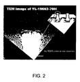
- FIG 2 is an SEM of a single geometry or hole on an electronic device substrate comprising a film deposited from TEOS after cleaning with the present invention.
- a new platform of low pH, fluoride stripper was provided for cleaning Cu/Low k patterned wafer. Compared with commercial fluoride strippers, this platform has lower pH value. Comparable clean performance, etch rates on metal / dielectric substrates with lower k-shift were observed with this formulation This formulaton provides lower k-shift after wet stripping compared to all commercial stripper products. This is used on Back End Of Line (BEOL) copper and porous low k dielectric film composites cleaning.
- An embodiment of the present invention stripper in accordance with this platform is set forth in Table 1, below. Table 1 YL-19662-70H Grams needed 100.00 DIW 90.00 Acetic Acid 0.50 PG 4.40 DPM 5.00 NH 4 F (40%) 0.10
- TEOS tetraethylorthosilicate
- pDEMS porous diethymethylsilane
- Dipropylene glycol monomethyl ether (DPM) and polyethylene glycol (PG) were added to help dissolve organic residue.
- Deionized water (DIW) is the predominant phase.
- Table 2 etch rate of YL-70H on various substrates Etch Rate (A/min)
- Cu AP pDEMS 2.5 TEOS (densified)
- TEOS (undensified) YL-19662-70H 4.5 0.1 0.1 0.15
- AP pDEMS 2.5 is a dielectric film deposited from diethoxymethylsilane and a porogen to produce a porous dielectric film when the porogen is removed to leave pores where the porogen was in the film, resulting in a dielectric value of 2.5.
- the diethoxymethylsilane and porogen are available from Air Products and Chemicals, Inc. of Allentown, PA, USA.
- carboxylic acids include, but are not limited to, acetic acid, propionic acid, butyric acid, valeric acid, octanoic acid, decanoic acid, dodecanoic acid, stearic acid, dodecanedioic acid, 2-methylheptanoic acid, 2-hexyldecanoic acid, oxalic acid, malonic acid, maleic acid, fumaric acid, succinic acid, itaconic acid, glutaric acid, adipic acid, malic acid, tartaric acid, acrylic acid, methacrylic acid, citric acid, lactic acid, glycolic, anthranilic acid, gallic acid, benzoic acid, isophthalic acid, phthalic acid, trimellitic acid, pyromellitic acid, salicylic acid, 2,4-dihydroxy benzoic acid and others.
- the carboxylic acid is a lower alkyl carboxylic acid.
- alkyl groups examples include; methyl, ethyl, propyl, isopropyl, butyl, isobutyl and tertbutyl.
- lower alkyl refers to alkyl groups of 1 to 4 carbon atoms.
- glycol ethers examples include ethylene glycol monomethyl ether, ethylene glycol monoethyl ether, ethylene glycol monobutyl ether, ethylene glycol dimethyl ether, ethylene glycol diethyl ether, diethylene glycol monomethyl ether, diethylene glycol monoethyl ether, diethylene glycol monopropyl ether, diethylene glycol monoisopropyl ether, diethylene glycol monobutyl ether, diethylene glycol monoisobutyl either, diethylene glycol monobenzyl ether, diethylene glycol dimethyl ether, diethylene glycol diethyl ether, triethylene glycol monomethyl ether, triethylene glycol dimethyl ether, polyethylene glycol monomethyl ether, diethylene glycol methyl ethyl ether, triethylene glycol ethylene glycol monomethyl ether acetate, ethylene glycol monethyl ether acetate, propylene glycol methyl ether acetate, propylene glycol methyl ether a
- Polyhydric alcohol used in the present invention are preferably mono- , di- or trialcohols, such as(C 4 - C 20 ) alkanols, (C 2 - C 20 ) alkanediols and (C 3 - C 20 ) alkanetriols, cyclic alcohols and substituted alcohols.
- Exemplary alcohols include; glycerol, ethylene glycol, propylene glycol, diethylene glycol, dipropylene glycol, hexylene glycol, 1,2-butandiol, 1,4-butandiol, 2,3-butandiol, benzyl alcohol, tetrahydrofurfuryl alcohol, 1-octanol, diacetone alcohol and 1, 4-cyclohexanedimethanol.
- Fluoride is present in the compositions described herein.
- Fluoride-containing compounds include those of the general formula R 1 R 2 R 3 R 4 NF where R 1 , R 2 , R 3 , and R 4 are independently hydrogen, an alcohol group, an alkoxy group, an alkyl group or mixtures thereof. Examples of such compounds are ammonium fluoride, tetramethyl ammonium fluoride, tetraethyl ammonium fluoride.
- Fluoroboric acid can also be used as the fluoride compounds. Still further examples of fluoride-containing compounds include fluoroboric acid, hydrofluoric acid, and choline fluoride.
- the fluoride is preferably present in amounts of from 0.001 % by weight to 20% by weight or from 0.1% by weight to 10% by weight.
- Ammonium fluoride is preferred in an amount of 0.01 wt% of a 40% concentration in water. In these embodiments, ammonium fluoride may be available commercially as a 40% aqueous solution.
- Water is present as an element of the present invention. It can be present coincidentally as a component of other elements of the invention such as an aqueous ammonium fluoride solution, or it can be added separately. Preferably, water is present in amounts of from 0.5% by weight to 90% by weight. In certain embodiments, the presence of water may improve the solubility of ammonium fluoride in the compositions of the present invention and aids in the removal of photoresist and cleaning of inorganic etch residues.
- Corrosion inhibitors in an amount of up to 20% by weight can be added to compositions of the present invention.
- the inhibitor concentration is from about 0.5% by weight to 8% by weight.
- Any corrosion inhibitor known in the art for similar applications, such as those disclosed in U.S. Pat. No. 5,417,877 which are incorporated herein by reference may be used.
- inhibitor compositions with a pKa greater than 6 do not function as well as inhibitor compositions having a pKa of less than about 6 in systems with a pH range of about 3 to about 6. Therefore, preferred inhibitor compositions are those having a pKa of about 6 or less.
- Corrosion inhibitors may be an organic acid, an organic acid salt, a phenol, a triazole, or a hydroxylamine.
- preferred inhibitor compositions include anthranilic acid, gallic acid, benzoic acid, isophthalic acid, maleic acid, fumaric acid, D,L-malic acid, malonic acid, phthalic acid, maleic anhydride, phthalic anhydride, carboxybenzotriazole, diethyl hydroxylamine and the lactic acid and citric acid salts thereof, and the like.
- corrosion inhibitors that may be used include catechol, pyrogallol, and esters of gallic acid.
- a pH ranging from about 3 to about 9, or ranging from about 3 to about 7, or ranging from about 3 to about 6 will allow most sensitive metals to passivate with minimum corrosion. Removal of highly inorganic etch residues and oxide skimming may require a slightly acidic pH. The pH of the composition disclosed herein is adjusted 3 for best efficacy for cleaning etch residue and passivation of metals.
- the invention further relates to the following items: 1.
- the formulation of Item 1 comprises deionized water, acetic acid, polyethylene glycol, dipropylene glycol monomethyl ether and ammonium fluoride.
- the formulation of Item 1 wherein the formulation contains the recited amounts of the components of the formulation: DIW 90.00 Acetic Acid 0.50 PG 4.40 DPM 5.00 NH 4 F (40%) 0.10 4.
- the formulation of Item 4 comprises deionized water, acetic acid, polyethylene glycol, dipropylene glycol monomethyl ether and ammonium fluoride.
- the process of Item 5 wherein the formulation contains the recited amounts of the components of the formulation: DIW 90.00 Acetic Acid 0.50 PG 4.40 DPM 5.00 NH 4 F (40%) 0.10
Landscapes
- Physics & Mathematics (AREA)
- General Physics & Mathematics (AREA)
- Cleaning Or Drying Semiconductors (AREA)
- Photosensitive Polymer And Photoresist Processing (AREA)
- Detergent Compositions (AREA)
- Drying Of Semiconductors (AREA)
- Weting (AREA)
Applications Claiming Priority (2)
| Application Number | Priority Date | Filing Date | Title |
|---|---|---|---|
| US3670708P | 2008-03-14 | 2008-03-14 | |
| US12/400,332 US20090229629A1 (en) | 2008-03-14 | 2009-03-09 | Stripper For Copper/Low k BEOL Clean |
Publications (1)
| Publication Number | Publication Date |
|---|---|
| EP2101219A1 true EP2101219A1 (de) | 2009-09-16 |
Family
ID=40873794
Family Applications (1)
| Application Number | Title | Priority Date | Filing Date |
|---|---|---|---|
| EP09003683A Withdrawn EP2101219A1 (de) | 2008-03-14 | 2009-03-13 | Abziehbad zur Kupfer/Low-k BEOL-Reinigung |
Country Status (6)
| Country | Link |
|---|---|
| US (1) | US20090229629A1 (de) |
| EP (1) | EP2101219A1 (de) |
| JP (1) | JP2009230134A (de) |
| KR (1) | KR20090098740A (de) |
| SG (1) | SG155852A1 (de) |
| TW (1) | TW200941160A (de) |
Families Citing this family (5)
| Publication number | Priority date | Publication date | Assignee | Title |
|---|---|---|---|---|
| CN101037646B (zh) * | 2003-08-27 | 2010-12-08 | 化研科技株式会社 | 除去助焊剂用洗涤剂及助焊剂的洗涤方法 |
| US8211844B2 (en) * | 2005-10-21 | 2012-07-03 | Freescale Semiconductor, Inc. | Method for cleaning a semiconductor structure and chemistry thereof |
| US7858572B2 (en) * | 2005-12-26 | 2010-12-28 | Liquid Technology Co., Ltd. | Composition for removing polymer residue of photosensitive etching-resistant layer |
| JP5827623B2 (ja) * | 2009-09-18 | 2015-12-02 | メルク パテント ゲゼルシャフト ミット ベシュレンクテル ハフツングMerck Patent Gesellschaft mit beschraenkter Haftung | インクジェット印刷可能なエッチングインク及び関連する方法 |
| JP7057653B2 (ja) * | 2017-12-08 | 2022-04-20 | 花王株式会社 | 樹脂マスク剥離用洗浄剤組成物 |
Citations (5)
| Publication number | Priority date | Publication date | Assignee | Title |
|---|---|---|---|---|
| US5417877A (en) | 1991-01-25 | 1995-05-23 | Ashland Inc. | Organic stripping composition |
| EP1548095A1 (de) * | 2002-09-30 | 2005-06-29 | Nippon Steel Corporation | Reinigungsmittel und reinigungsverfahren für baustoffe aus titan und titanlegierung zwecks entfernung von verfärbungen |
| EP1612858A2 (de) * | 2004-07-01 | 2006-01-04 | Air Products And Chemicals, Inc. | Zusammensetzung zum Abziehen und Reinigen und deren Verwendung |
| EP1736534A1 (de) * | 2005-06-23 | 2006-12-27 | Air Products and Chemicals, Inc. | Zusammensetzung und Verfahren zur Rückstandsentfernung |
| WO2008157345A2 (en) * | 2007-06-13 | 2008-12-24 | Advanced Technology Materials, Inc. | Wafer reclamation compositions and methods |
Family Cites Families (7)
| Publication number | Priority date | Publication date | Assignee | Title |
|---|---|---|---|---|
| US6828289B2 (en) * | 1999-01-27 | 2004-12-07 | Air Products And Chemicals, Inc. | Low surface tension, low viscosity, aqueous, acidic compositions containing fluoride and organic, polar solvents for removal of photoresist and organic and inorganic etch residues at room temperature |
| JP2001100436A (ja) * | 1999-09-28 | 2001-04-13 | Mitsubishi Gas Chem Co Inc | レジスト剥離液組成物 |
| ATE431844T1 (de) * | 2002-02-11 | 2009-06-15 | Rhodia Chimie Sa | Waschmittel mit blockcopolymer |
| US7166419B2 (en) * | 2002-09-26 | 2007-01-23 | Air Products And Chemicals, Inc. | Compositions substrate for removing etching residue and use thereof |
| TWI362415B (en) * | 2003-10-27 | 2012-04-21 | Wako Pure Chem Ind Ltd | Novel detergent and method for cleaning |
| KR101238471B1 (ko) * | 2005-02-25 | 2013-03-04 | 이케이씨 테크놀로지, 인코포레이티드 | 구리 및 저 k 유전체 물질을 갖는 기판으로부터 레지스트,에칭 잔류물 및 구리 산화물을 제거하는 방법 |
| US20070179072A1 (en) * | 2006-01-30 | 2007-08-02 | Rao Madhukar B | Cleaning formulations |
-
2009
- 2009-03-09 US US12/400,332 patent/US20090229629A1/en not_active Abandoned
- 2009-03-13 KR KR1020090021621A patent/KR20090098740A/ko not_active Ceased
- 2009-03-13 SG SG200901759-1A patent/SG155852A1/en unknown
- 2009-03-13 TW TW098108334A patent/TW200941160A/zh unknown
- 2009-03-13 JP JP2009062004A patent/JP2009230134A/ja active Pending
- 2009-03-13 EP EP09003683A patent/EP2101219A1/de not_active Withdrawn
Patent Citations (5)
| Publication number | Priority date | Publication date | Assignee | Title |
|---|---|---|---|---|
| US5417877A (en) | 1991-01-25 | 1995-05-23 | Ashland Inc. | Organic stripping composition |
| EP1548095A1 (de) * | 2002-09-30 | 2005-06-29 | Nippon Steel Corporation | Reinigungsmittel und reinigungsverfahren für baustoffe aus titan und titanlegierung zwecks entfernung von verfärbungen |
| EP1612858A2 (de) * | 2004-07-01 | 2006-01-04 | Air Products And Chemicals, Inc. | Zusammensetzung zum Abziehen und Reinigen und deren Verwendung |
| EP1736534A1 (de) * | 2005-06-23 | 2006-12-27 | Air Products and Chemicals, Inc. | Zusammensetzung und Verfahren zur Rückstandsentfernung |
| WO2008157345A2 (en) * | 2007-06-13 | 2008-12-24 | Advanced Technology Materials, Inc. | Wafer reclamation compositions and methods |
Also Published As
| Publication number | Publication date |
|---|---|
| SG155852A1 (en) | 2009-10-29 |
| US20090229629A1 (en) | 2009-09-17 |
| KR20090098740A (ko) | 2009-09-17 |
| TW200941160A (en) | 2009-10-01 |
| JP2009230134A (ja) | 2009-10-08 |
Similar Documents
| Publication | Publication Date | Title |
|---|---|---|
| KR100700998B1 (ko) | 기판으로부터 잔사를 제거하기 위한 조성물 및 그의 사용방법 | |
| JP4814356B2 (ja) | はく離及び洗浄用の組成物並びにそれらの使用 | |
| EP2098911B1 (de) | Abbeizmittel zur Trockenfilmentfernung und Verfahren zu dessen Anwendung | |
| KR100595024B1 (ko) | 박리제 조성물 | |
| JP4918939B2 (ja) | 半導体ドライプロセス後の残渣除去液及びそれを用いた残渣除去方法 | |
| KR100942009B1 (ko) | 포토레지스트, 에칭 잔류물 및 barc를 제거하기 위한제제 | |
| TW200411326A (en) | Removing solution | |
| TW200521222A (en) | Lactam compositions for cleaning organic and plasma etched residues for semiconductor devices | |
| TWI375988B (en) | Aqueous solution for the removal of post-ethc residue | |
| KR102242918B1 (ko) | 식각액 조성물 | |
| EP1688798A2 (de) | Rückstandentferner auf wässriger Basis mit Fluorid | |
| EP2101219A1 (de) | Abziehbad zur Kupfer/Low-k BEOL-Reinigung | |
| JP2012046685A (ja) | 洗浄組成物、これを用いた洗浄方法及び半導体素子の製造方法 | |
| KR20180030581A (ko) | 세정 조성물 및 이의 사용 방법 | |
| US20040018949A1 (en) | Semiconductor process residue removal composition and process | |
| EP1883863B1 (de) | Zusammensetzung zur entfernung von nach-ätz- und aschen-fotoresistresten und massivem fotoresist | |
| CN102132385B (zh) | 半导体干式工艺后的残渣除去液和使用该除去液的残渣除去方法 | |
| KR20200070410A (ko) | 플루오라이드를 기초로 한 세정 조성물 | |
| US20120172272A1 (en) | Cleaning composition for semiconductor device and method of cleaning semiconductor device using the same | |
| US20240392194A1 (en) | Post-Dry Etching Photoresist And Metal Containing Residue Removal Formulation | |
| CN117590709A (zh) | 去除半导体基材灰化后残留物与光阻剂的组合物及方法 | |
| JP5574795B2 (ja) | 半導体基板の洗浄方法 | |
| JP5498843B2 (ja) | 2剤型半導体基板用洗浄剤 | |
| CN101544931A (zh) | 用于铜/低k后段制程清洗的清除剂 | |
| KR20160044852A (ko) | 금속막용 세정제 조성물 |
Legal Events
| Date | Code | Title | Description |
|---|---|---|---|
| PUAI | Public reference made under article 153(3) epc to a published international application that has entered the european phase |
Free format text: ORIGINAL CODE: 0009012 |
|
| AK | Designated contracting states |
Kind code of ref document: A1 Designated state(s): AT BE BG CH CY CZ DE DK EE ES FI FR GB GR HR HU IE IS IT LI LT LU LV MC MK MT NL NO PL PT RO SE SI SK TR |
|
| AX | Request for extension of the european patent |
Extension state: AL BA RS |
|
| AKX | Designation fees paid | ||
| STAA | Information on the status of an ep patent application or granted ep patent |
Free format text: STATUS: THE APPLICATION IS DEEMED TO BE WITHDRAWN |
|
| 18D | Application deemed to be withdrawn |
Effective date: 20100317 |
|
| REG | Reference to a national code |
Ref country code: DE Ref legal event code: 8566 |