EP2101357A2 - Module d'énergie solaire disposant d'une ligne de réparation, ensemble d'énergie solaire en disposant, procédé de réparation du module d'énergie solaire et procédé de réglage de l'ensemble d'énergie solaire - Google Patents
Module d'énergie solaire disposant d'une ligne de réparation, ensemble d'énergie solaire en disposant, procédé de réparation du module d'énergie solaire et procédé de réglage de l'ensemble d'énergie solaire Download PDFInfo
- Publication number
- EP2101357A2 EP2101357A2 EP20090003514 EP09003514A EP2101357A2 EP 2101357 A2 EP2101357 A2 EP 2101357A2 EP 20090003514 EP20090003514 EP 20090003514 EP 09003514 A EP09003514 A EP 09003514A EP 2101357 A2 EP2101357 A2 EP 2101357A2
- Authority
- EP
- European Patent Office
- Prior art keywords
- solar energy
- unit cell
- repair
- electrode layer
- module
- Prior art date
- Legal status (The legal status is an assumption and is not a legal conclusion. Google has not performed a legal analysis and makes no representation as to the accuracy of the status listed.)
- Granted
Links
Images


Classifications
-
- H—ELECTRICITY
- H10—SEMICONDUCTOR DEVICES; ELECTRIC SOLID-STATE DEVICES NOT OTHERWISE PROVIDED FOR
- H10F—INORGANIC SEMICONDUCTOR DEVICES SENSITIVE TO INFRARED RADIATION, LIGHT, ELECTROMAGNETIC RADIATION OF SHORTER WAVELENGTH OR CORPUSCULAR RADIATION
- H10F19/00—Integrated devices, or assemblies of multiple devices, comprising at least one photovoltaic cell covered by group H10F10/00, e.g. photovoltaic modules
-
- H—ELECTRICITY
- H02—GENERATION; CONVERSION OR DISTRIBUTION OF ELECTRIC POWER
- H02S—GENERATION OF ELECTRIC POWER BY CONVERSION OF INFRARED RADIATION, VISIBLE LIGHT OR ULTRAVIOLET LIGHT, e.g. USING PHOTOVOLTAIC [PV] MODULES
- H02S40/00—Components or accessories in combination with PV modules, not provided for in groups H02S10/00 - H02S30/00
- H02S40/30—Electrical components
- H02S40/36—Electrical components characterised by special electrical interconnection means between two or more PV modules, e.g. electrical module-to-module connection
-
- H—ELECTRICITY
- H02—GENERATION; CONVERSION OR DISTRIBUTION OF ELECTRIC POWER
- H02S—GENERATION OF ELECTRIC POWER BY CONVERSION OF INFRARED RADIATION, VISIBLE LIGHT OR ULTRAVIOLET LIGHT, e.g. USING PHOTOVOLTAIC [PV] MODULES
- H02S50/00—Monitoring or testing of PV systems, e.g. load balancing or fault identification
- H02S50/10—Testing of PV devices, e.g. of PV modules or single PV cells
-
- H—ELECTRICITY
- H10—SEMICONDUCTOR DEVICES; ELECTRIC SOLID-STATE DEVICES NOT OTHERWISE PROVIDED FOR
- H10F—INORGANIC SEMICONDUCTOR DEVICES SENSITIVE TO INFRARED RADIATION, LIGHT, ELECTROMAGNETIC RADIATION OF SHORTER WAVELENGTH OR CORPUSCULAR RADIATION
- H10F19/00—Integrated devices, or assemblies of multiple devices, comprising at least one photovoltaic cell covered by group H10F10/00, e.g. photovoltaic modules
- H10F19/30—Integrated devices, or assemblies of multiple devices, comprising at least one photovoltaic cell covered by group H10F10/00, e.g. photovoltaic modules comprising thin-film photovoltaic cells
- H10F19/31—Integrated devices, or assemblies of multiple devices, comprising at least one photovoltaic cell covered by group H10F10/00, e.g. photovoltaic modules comprising thin-film photovoltaic cells having multiple laterally adjacent thin-film photovoltaic cells deposited on the same substrate
-
- H—ELECTRICITY
- H10—SEMICONDUCTOR DEVICES; ELECTRIC SOLID-STATE DEVICES NOT OTHERWISE PROVIDED FOR
- H10F—INORGANIC SEMICONDUCTOR DEVICES SENSITIVE TO INFRARED RADIATION, LIGHT, ELECTROMAGNETIC RADIATION OF SHORTER WAVELENGTH OR CORPUSCULAR RADIATION
- H10F19/00—Integrated devices, or assemblies of multiple devices, comprising at least one photovoltaic cell covered by group H10F10/00, e.g. photovoltaic modules
- H10F19/90—Structures for connecting between photovoltaic cells, e.g. interconnections or insulating spacers
-
- H—ELECTRICITY
- H10—SEMICONDUCTOR DEVICES; ELECTRIC SOLID-STATE DEVICES NOT OTHERWISE PROVIDED FOR
- H10F—INORGANIC SEMICONDUCTOR DEVICES SENSITIVE TO INFRARED RADIATION, LIGHT, ELECTROMAGNETIC RADIATION OF SHORTER WAVELENGTH OR CORPUSCULAR RADIATION
- H10F77/00—Constructional details of devices covered by this subclass
- H10F77/93—Interconnections
- H10F77/933—Interconnections for devices having potential barriers
- H10F77/935—Interconnections for devices having potential barriers for photovoltaic devices or modules
- H10F77/937—Busbar structures for modules
-
- Y—GENERAL TAGGING OF NEW TECHNOLOGICAL DEVELOPMENTS; GENERAL TAGGING OF CROSS-SECTIONAL TECHNOLOGIES SPANNING OVER SEVERAL SECTIONS OF THE IPC; TECHNICAL SUBJECTS COVERED BY FORMER USPC CROSS-REFERENCE ART COLLECTIONS [XRACs] AND DIGESTS
- Y02—TECHNOLOGIES OR APPLICATIONS FOR MITIGATION OR ADAPTATION AGAINST CLIMATE CHANGE
- Y02E—REDUCTION OF GREENHOUSE GAS [GHG] EMISSIONS, RELATED TO ENERGY GENERATION, TRANSMISSION OR DISTRIBUTION
- Y02E10/00—Energy generation through renewable energy sources
- Y02E10/50—Photovoltaic [PV] energy
Definitions
- the present disclosure of invention relates to a solar energy module, a solar energy assembly having the solar energy module, a method of repairing the solar energy module and a method of trimming the solar energy assembly. More particularly, the disclosure relates to a solar energy module which includes unit cells of a thin-film type.
- a solar energy module of a thin-film type (e.g., amorphous silicon) includes a plurality of unit cells which are connected in series with each other where each operative unit cell generates electrical energy at a respective voltage in response to absorbed solar radiation.
- the unit cells may be integrally formed on a glass substrate through an integrated circuit batch process.
- a solar energy module having a defect such as mentioned above may not be suitable for use in fields requiring long term reliability. For example, even after manufacture of an almost fully operable module but with one defective cell (or but with a short run burst of defects such as in a few immediately-adjacent-to-each-other cells), the entire solar energy module may become unusable for its intended purpose and may have to be discarded despite the fact that it contains a substantially large number of good cells.
- an efficient method of detecting defects and repairing the solar energy module can be devised, it may be possible to avoid the need for discarding an entire solar energy module due to only a single cell defect or a spot-like defect wherein just a few close together cells are defective.
- a solar energy assembly typically includes a plurality of such solar energy modules which are connected in parallel with each other so that their currents may be summed. If the module output voltages of each of the solar energy modules are not uniformly essentially the same, the long-term reliability of the solar energy modules may be decreased due to large short circuiting currents flowing among the parallel-wise connected circuits that have substantially different output voltages.
- the output voltages of each of the unit cells on that one substrate tend to be nearly the same as each other.
- About 50 to 100 of the unit cells are typically connected in series with each other on the integrated substrate to form the integrated solar energy module.
- the output voltage of each of the unit cells has a variation of about ⁇ 5% due to variations in the manufacturing process.
- This variation of the output voltage of a single unit cell may be very small, however, the variation of the output voltage of a large number of unit cells (in other words, of a module) may be on the order about several volts.
- the solar energy modules are connected in parallel in an electrical power generation system.
- the module output voltages it is desirable for the module output voltages to be uniform with one another for long-term reliability. Accordingly, in addition to a method of repairing when defective unit cells are present, a method for preventing or controlling the variations of the parallel-wise connected solar energy modules is desired.
- the present disclosure of invention provides a monolithically integrated solar energy module in which repair may be easily effected for individual defective unit cells or for groups of defective unit cells and/or in which individual module voltage output may be easily trimmed to match a predefined reference voltage.
- Example embodiments of the present disclosure also include a solar energy assembly including a plurality of solar energy modules connected in parallel to one another.
- Example embodiments of the present disclosure also include a method of repairing a solar energy module having one or more defective cells.
- Example embodiments of the present disclosure also include a method of trimming modules in the solar energy assembly so that they are substantially matched with one another.
- a solar energy module includes a plurality of unit cells that are connected in series and an integrated bypass line extending alongside the series of unit cells.
- Each unit cell includes a set of integrated electrode layers, a set of one or more integrated semiconductor layers and an integrated repair pad.
- the set of integrated electrode layers includes a lower electrode layer and a spaced apart upper electrode layer facing the lower electrode layer.
- the set of semiconductor layers is disposed between the lower electrode layer and the upper electrode layer and defines a photo-electric converter that converts photonic energy into electrical energy.
- the repair pad is electrically connected to the electrode layer and protrudes toward one side of the cell unit.
- An electrode layer of a first unit cell is electrically connected to an electrode layer of a next adjacent unit cell, if any, so that the successive unit cells are thereby connected in series with each other.
- the bypass line is disposed closely adjacent to a plurality of the repair pads so as to function for each unit cell as said other adjacent structure to which the respective repair pad of the unit cell may be connected.
- a solar energy assembly includes a plurality of solar energy modules, a first output line and a second output line.
- Each of the solar energy modules includes an array of successively connected unit cells, a first bypass line and a second bypass line.
- Each of the unit cells includes a set of electrode layers including a lower electrode layer and an upper electrode layer facing each other, a set of one or more semiconductor layers disposed between the lower electrode layer and the upper electrode layer, and a repair pad being electrically connected to an electrode layer of the set of electrode layers and protruding outwardly from one side of the unit cell.
- the upper electrode layer of a first unit cell is integrally connected to a lower electrode layer of a next adjacent unit cell, if any, so that the unit cells are integrally connected in series with each other.
- the first bypass line extends adjacent to the repair pad of the unit cell corresponding to a high-voltage output of the array.
- the second bypass line extends adjacent to the repair pad of the unit cell corresponding to a low-voltage output of the array where the difference between the high and low voltages is substantially equal to a pre-defined reference voltage.
- the first output line connects the respective repair pads corresponding to the high-voltage output of the solar energy modules in parallel with each other.
- the second output line connects the respective repair pads corresponding to the low-voltage output of the solar energy modules in parallel with each other.
- the method includes at least one of performing a first bypassing and performing a second bypassing.
- the first bypassing includes connecting repair pads extending from electrode layers of a first unit cell and a second unit cell to a bypass line so that one or more unit cells including the first unit cell or the second unit cell are bypassed.
- the second bypassing includes directly connecting repair pads of a third unit cell and a fourth unit cell with each other so that at least one of the third unit cell and the fourth unit cell is bypassed.
- each of the solar energy modules includes an array of successive unit cells.
- An upper electrode layer which is disposed on a corresponding one or more semiconductor layers of each unit cell where the semiconductor layers define a photo-electric converter, and the upper electrode layer of a first of the cells is electrically connected to a lower electrode layer under semiconductor layers of a next adjacent unit cell along a first direction, so that the successive unit cells are thereby connected in series with each other.
- a reference output voltage for the solar energy modules is defined as a voltage which is to be substantially output by all for the solar energy modules of the assembly where necessary bypassing one or more cells in each repairing each of the solar energy modules so as to thereby cause each to have the reference output voltage.
- Respective voltage outputs of the solar energy modules are connected parallel with each other by using output lines of the solar energy modules.
- the defective unit cell when a defective unit cell is detected after forming a solar energy module by forming a thin film during a mass production process, the defective unit cell may be bypassed so that the yield of operable modules may be increased.
- the module output voltage may become uniform so that the reliability of the module may be increased when combined with other modules.
- FIG. 1 is a plan view illustrating a solar energy module in accordance with an embodiment
- FIG. 2 is a cross-sectional view illustrating the solar energy module taken along a line I-I' in FIG. 1 ;
- FIG. 3 is a cross-sectional view illustrating the solar energy module taken along a line II-II' in FIG 1 ;
- FIG. 4 is an equivalent circuit diagram for the unit cell in FIG. 2 ;
- FIG. 5 is a flowchart illustrating a method of repairing the solar energy module in accordance with a first embodiment
- FIG. 6 is a cross-sectional view illustrating an example method of testing the unit cell for defects
- FIG. 7 is a cross-sectional view illustrating another example method of testing the unit cell for defects
- FIG. 8 is a graph of a current generated from the unit cell in relation to a test voltage applied to the unit cell as illustrated in FIGS. 6 and 7 ;
- FIG. 9 is a plan view of the solar energy module repaired according to one or more methods described in FIGS. 5 and 9 ;
- FIG. 10 is an equivalent circuit diagram illustrating the solar energy module in FIG. 9 ;
- FIG. 11 is a plan view illustrating a first embodiment of a solar energy assembly in accordance with the disclosure.
- FIG. 12 is an equivalent circuit diagram illustrating the solar energy assembly in FIG. 11 ;
- FIG. 13 is a flowchart illustrating a method of trimming the solar energy assembly of Fig. 11 ;
- FIG. 14 is a plan view illustrating a solar energy assembly including solar energy modules which may be trimmed to have substantially the same module output voltages as each other;
- FIG. 15 is an enlarged view illustrating a first area, A in FIG. 14 ;
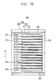
- FIG. 16 is a plan view illustrating a second embodiment of a solar energy module in accordance with the disclosure.
- FIG. 17 is a plan view illustrating a solar energy assembly including solar energy modules which may be trimmed to have substantially the same module output voltage as each other in accordance with a second embodiment
- FIG. 18 is an enlarged view illustrating a second area, B in FIG. 17 ;
- FIG. 19 is a plan view illustrating a solar energy module in accordance with another example embodiment.
- FIG. 20 is a cross-sectional view illustrating the solar energy module taken along a line III-III' in FIG. 19 ;
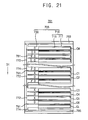
- FIG. 21 is a plan view illustrating a solar energy module in accordance with still another example embodiment
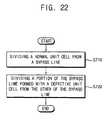
- FIG. 22 is a flowchart illustrating method of repairing the solar energy module in FIG. 21 ;
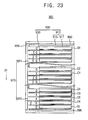
- FIG. 23 is a plan view illustrating a solar energy module in accordance with a fifth embodiment.
- first, second, third etc. may be used herein to describe various elements, components, regions, layers and/or sections, these elements, components, regions, layers and/or sections should not be limited by these terms. These terms are only used to distinguish one element, component, region, layer or section from another region, layer or section. Thus, a first element, component, region, layer or section discussed below could be termed a second element, component, region, layer or section without departing from the teachings of the present invention.
- spatially relative terms such as “beneath,” “below,” “lower,” “above,” “upper” and the like, may be used herein for ease of description to describe one element or feature's relationship to another element(s) or feature(s) as illustrated in the figures. It will be understood that the spatially relative terms are intended to encompass different orientations of the device in use or operation in addition to the orientation depicted in the figures. For example, if the device in the figures is turned over, elements described as “below” or “beneath” other elements or features would then be oriented “above” the other elements or features. Thus, the exemplary term “below” can encompass both an orientation of above and below. The device may be otherwise oriented (rotated 90 degrees or at other orientations) and the spatially relative descriptors used herein interpreted accordingly.
- Exemplary embodiments are described herein with reference to cross-sectional illustrations that are schematic illustrations of idealized example embodiments (and intermediate structures) of the present invention. As such, variations from the shapes of the illustrations as a result, for example, of manufacturing techniques and/or tolerances, are to be expected. Thus, example embodiments herein should not be construed as limited to the particular shapes of regions illustrated herein but are to include deviations in shapes that result, for example, from manufacturing. For example, an implanted region illustrated as a rectangle will, typically, have rounded or curved features and/or a gradient of implant concentration at its edges rather than a binary change from implanted to non-implanted region.
- a buried region formed by implantation may result in some implantation in the region between the buried region and the surface through which the implantation takes place.
- the regions illustrated in the figures are schematic in nature and their shapes are not intended to illustrate the actual shape of a region of a device and are not intended to limit the scope of the present invention.
- FIG. 1 is a plan view illustrating a solar energy module 1 in accordance with a first embodiment.
- FIG. 2 is a cross-sectional view illustrating the solar energy module 1 taken along a line I-I' in FIG. 1 .
- the solar energy module 1 includes a plurality of horizontally extending unit cells 5 and a vertically extending bypass line 70, both integrally formed on a monolithic substrate 50.
- Operative normal ones of the unit cells 5 can generate electrical power in response to externally supplied incident light such as the solar light shown entering from the bottom of the electrically-insulating and light-passing substrate 50 in Fig. 2 .
- the horizontal unit cells 5 are disposed one after another along a first vertical direction D1 (vertical in Fig. 1 ) and they are initially all electrically connected in series with each other along that first direction D1.
- the solar energy module 1 is formed of a thin film construct (e.g., it uses thin films of amorphous silicon as its active layer).
- the solar energy module 1 includes a light passing (e.g., transparent) and electrically insulating substrate 50 such as a glass substrate or a plastic one or a combination of both.
- Each of the unit cells 5 includes a set of electrodes referenced as 10 and disposed on the substrate 50, a plurality of semiconductor layers referenced as 20 and a local repair pad 30 (where the lead line of reference number 30 terminates at the top edge of the repair pad in Fig. 1 ).
- the electrode set 10 includes a lower electrode layer 11 and an upper electrode layer 15 (where the respective lead lines of reference numbers 11, 15 terminate at the top edges of the respective lower and upper electrode layers in Fig. 1 ).
- the lower electrode layer 11 is formed on an upper face of the substrate 50 and may be formed of transparent and electrically conductive materials, for example, one or more transparent conductive oxides (TCO's, e.g., ITO, IZO, etc.).
- TCO's transparent conductive oxides
- the upper electrode layer 15 is disposed above the lower electrode layer 11 and facing the lower electrode layer 11.
- the upper electrode layer 15 may be formed to include a light reflecting metal (e.g., reflective aluminum).
- the upper electrode layer 15 may function as a light reflecting electrode.
- the set of semiconductor layers 20 is disposed between the lower electrode layer 11 and the upper electrode layer 15.
- the semiconductor layers set 20 can generate an electromotive force (e.g., a voltage) in response to absorbed incident light such as solar light transmitted through the substrate 50 and through the lower electrode layer 11.
- An electric field may be formed between the lower electrode layer 11 and the upper electrode layer 15 due to the electromotive force, so that an electric current may be generated by the unit cells 5 when connected to an appropriate load.
- the type of semiconductors used in layer 20 may be varied.
- the illustrated set of semiconductor layers 20 may define a PIN junction diode.
- Such a PIN diode may be formed by stacking a P-type semiconductor layer 21 (e.g., a-Si), an intrinsic (I-type) semiconductor layer 23 and an N-type semiconductor layer 25 according to this recited order to form the semiconductor layers set 20. (Although not explicitly shown in Fig.
- vertical sidewall faces (e.g., 7) of the stacked semiconductor layers are insulated for example by a thin oxide (not shown) so as to prevent shorting through adjacent vertical sides of electrodes 11 and 15.
- the semiconductor layers set 20 may define an optical absorption diode which absorbs light and responsively generates an electrical voltage and/or current, a unit cell 5 is formed.
- the currents and/or voltages generated by the respective unit cells 5 may be collected through output lines which are connected to selected ones of the lower electrode layers 11 and the upper electrode layers 15, respectively.
- the electrode set 10 and the semiconductor layers set 20 may be formed on the substrate 50 by using thin-film deposition processes.
- a cell-to-cell separation space 27 may be formed through the upper electrode layer 15 and through the semiconductor layers set 20, where separation space 27 is periodically repeated along the D1 direction as illustrated in FIG. 2 .
- the unit cells 5 are thus separated from each other by the cell-to-cell separation spaces 27.
- First insulating sidewalls (not shown) may be formed on the inside walls of each cell-to-cell separation spaces for providing electrical insulation.
- each of the unit cells 5 may have a width about 1 cm (as measured in the D 1 direction of Fig. 2 ) and a length about 1 m or more (in other words, an aspect ratio of about 1:100 or more).
- each of the unit cells 5 may have the shape of an elongated rectangle or bar as seen in Fig. 1 .
- the unit cells 5 are electrically connected in series with each other along the first direction D1 which is substantially perpendicular to the longitudinal axes of the unit cells 5.
- the upper electrode layer 15 of a first of the unit cells 5 may be electrically connected to the lower electrode layer 11 of an adjacent second of the unit cells 5 along the first direction D1 as is schematically illustrated in FIG. 2 .
- Each contact hole 26 is formed through the semiconductor layers set 20, so that the lower electrode layer 11 is partially exposed at the bottom of the otherwise insulated contact hole 26 (into which hole, electrode layer 15 descends).
- the upper electrode layer 15 of the adjacent unit cell 5 extends down to the bottom of the contact hole 26 so as to be electrically connected to the lower electrode layer 11 of the next cell along the D1 direction (to its right as shown in Fig. 2 ).
- insulating sidewalls Prior to deposition of layer 15, insulating sidewalls (not shown) may be formed on the insides of each contact hole 26 so as to thereby insulate the semiconductor layers set 20 from the portion of the upper electrode layer 15 that descends down into contact hole 26.
- An electrode separation gap 8 is formed between the adjacent lower electrode layers, for example by use of sidewall insulating material.
- the semiconductor layers set 20 may extend into the electrode separation gap 8 without making sidewall contact with the adjacent lower electrodes 11 and 11' (the prime indicating the next cell in the D1 direction).
- Gap insulating layers (not shown) may be formed on inside of each electrode separation gap 8 to insulate the semiconductor layers set 20 and the lower electrode 11 between the adjacent unit cells 5.
- FIG. 3 is a cross-sectional view illustrating the solar energy module 1 taken along a line II-II' in FIG. 1 .
- the repair pad 30 protrudes from the electrode set 10 along the cell's longitudinal axis toward one side of the unit cell 5.
- the repair pad 30 is integrally formed seamlessly with, or is otherwise electrically connected to the lower electrode layer 11.
- the repair pad 30 extends beyond the lower electrode 11 along the cell's longitudinal axis direction and thus protrudes in an exposed manner from the end portion of the unit cell 5.
- the lower electrode layer 11 and the repair pad 30 may be formed from a same material (e.g., ITO, IZO, etc.).
- the repair pads 30 of two adjacent cells may be used to bypass (e.g., short out) a single defective unit cell 5 among the adjacent cells and to thus provide a repair for the defect.
- to repair a defect refers to creating a cell-bypassing closed circuit connection around the defective unit cell 5 while leaving the rest of the array of the unit cells 5 connected to each other in series and thus allowing the remaining nondefective cells to operate in series while electrically bypassing the defective (e.g., open) unit cell 5.
- the aforementioned bypass line 70 is formed closely adjacent to, but spaced apart from the plurality of repair pads 30 of the respective unit cells 5.
- the bypass line or conductor 70 may extend along the first direction D1 (vertical in Fig. 1 ) and may include narrow sections as well as wide sections as shown in Fig. 1 .
- the integrated bypass line 70 may be used to bypass the row of the identified defective unit cell 5.
- the bypass line 70 and the repair pads 30 may be formed on the same layer or on different layers of the substrate 50. When the bypass line 70 and the repair pads 30 are formed on the same layer, repair processes for the defective unit cell 5 may become more efficient.
- the solar energy module 1 may further include a first module output line 93 and a second module output line 95.
- the first output line 93 (where the lead line of reference number 93 terminates at the top edge of the first module output line in Fig. 1 ) is integrally connected to the module's topmost repair pad 30, where the latter corresponds to a maximum high-voltage output of the solar energy module 1.
- the second module output line 95 (where the lead line of reference number 95 terminates at the bottom edge of the second module output line in Fig. 1 ) is integrally connected to the module's lowermost repair pad 30 where the latter corresponds to a lowest output voltage (e.g., ground or negative) of the solar energy module 1.
- the first output line 93 and the second output line 95 may be directly connected to the repair pads 30 of the top unit cell 5 and the bottom unit cell 5 respectively rather than through the bypass line 70.
- the vertical bypass line 70 is directly connected to the top and bottom module output lines, 393, 395 and cuts are made into the vertical bypass line 70 at the points where it is strap-wise connected to a topmost and bottommost cell of the array.
- FIG. 4 is an equivalent circuit diagram for the unit cell 5 in FIG. 2 and is used for explaining some of the different kinds of defects that may occur.
- the semiconductor layers set 20 is represented as the optical absorption diode 20 which absorbs light and generates a corresponding electromotive force resulting in the production of current J Light .
- the same reference number 20 is used for the optical absorption diode 20 and the semiconductor layers 20.
- a contact series resistor, R-series is effectively formed at an interface between the lower electrode layer 11 and the P-type semiconductor layer 21 and/or at an interface between the upper electrode layer 15 and the N-type semiconductor layer 25.
- the contact resistor, R-series is an internal resistance of the unit cell 5 and is thus connected in series with the idealized optical absorption diode 20 as illustrated in FIG. 4 .
- the cell generated voltage which appears between the lower electrode layer 11 and the upper electrode layer 15 may have a lower voltage level (V) than that of the internal electromotive force (V + IR) produced by the diode 20 due to the ohmic drop (I*R) of the contact resistor, R-series.
- V voltage level
- I*R ohmic drop
- a first current Ij outputted from the internal diode 20 will be increased when the resistance of the contact resistor R-series is decreased and diode voltage remains unchanged.
- the resistance of the contact resistance, R-series of a normal unit cell 5 may be very small.
- a defective cell may have a substantially greater contact resistor, R-series which disadvantageously impedes flow of series current through the series connected array of plural diodes.
- a portion of the ideal current, I J generated by each ideal diode 20 may fail to be drawn out at the output terminal (V, I) and instead may be lost as shunt loss current I rsh through a parasitic shunt resistance, R shunt .
- a portion of the generated current may be leaked along cell side faces 7 of the cell-to-cell separation space 27 and may be leaked along the electrode separation gap 8 as illustrated in FIG. 2 .
- the resistance of the effective shunt resistance (R-shunt) in good cells may be very large, so that loss due to this mechanism is substantially negligible. As seen in Fig. 4 , this loss mechanism is referred to as a leakage resistor R-shunt and the leakage resistor R-shunt is connected in parallel with the optical absorption diode 20.
- the cell output current I is substantially the same as the ideal current I J output by the optical absorption diode 20.
- each repair pad 30 extends from the lower electrode layer 11 toward one side of the respective unit cell 5 and toward the bypass line 70 where the vertical bypass line 70 is disposed to be closely adjacent to and normally spaced apart and insulated from the repair pads 30, but where the spacing may be conveniently closed by one or more means so as to thereby connect the unit cell 5 to the adjacent bypass line 70.
- FIG. 5 is a flowchart illustrating an exemplary method of repairing the solar energy module in accordance with a first embodiment by using the repair pads 30 and/or the adjacent bypass line 70.
- the method of repairing the solar energy module may be used in repairing the solar energy module 1 of FIGS. 1 to 4 .
- the method of repairing at least one of a first bypassing and a second bypassing is performed.
- the performing order for the first bypassing and the second bypassing may be varied and repeated as deemed appropriate.
- the repair pads 30 of a first unit cell 5 and a second unit cell 5 are connected to the bypass line 70 so that one or more unit cells 5 including at least one of the first unit cell 5 or the second unit cell 5 are bypassed (step S10).
- each unit cell 5 is inspected to determine if the unit cell 5 is a defective unit cell 5.
- a defective unit cell 5 may be deemed as such if it fails to have desired properties substantially close to that of the ideal optical absorption diode 20 and its associated series and shunt resistances (R series , R shunt ). Inspection and determination may be carried out by automated means such as by automated test equipment (ATE) with appropriate computer software controlling the inspection and the subsequent repair process if needed.
- ATE automated test equipment
- One method by which it may be determined whether a given unit cell 5 has any defects or not is by determining whether an I versus V graph (see Fig. 8 ) for that cell shows a current outputted from the unit cell 5 in relation to a potential difference formed between the lower electrode layer 11 and the upper electrode layer 15 as substantially following a desired rectification graph of a current in relation to voltage for an ideal diode 20 or not.
- FIG. 6 is a cross-sectional view illustrating a first example method of testing a corresponding unit cell 5 for defects.
- FIG. 7 is a cross-sectional view illustrating another example method of testing the unit cell 5 for defects.
- a set of probes 104 may be used to test the unit cell 5.
- the probes 104 are contacted with the upper electrode layers 15 adjacent to each other, respectively, and a varied test voltage (V) may be applied between the upper electrode layers 15 as illustrated in FIG. 6 while resulting current (I) is measured (or vise versa).
- V test voltage
- I current
- the probes 104 are contacted with the lower electrode layers 11 (e.g., to pads 30) adjacent to each other, respectively, and the test voltage may be applied to the lower electrode layers 11 as illustrated in FIG. 7 .
- the upper electrode layer 15 of one of the unit cells 5 of the solar energy module 1 illustrated in FIGS. 1 to 4 is electrically connected to the lower electrode layer 11 of another one of the unit cells 5 adjacent to the one of the unit cells 5 along the first direction D1.
- the test voltage is applied to the lower electrode layer 11 and the upper electrode layer 15 of the same unit cell 5.
- FIG. 8 shows a variety of possible graphs of a measured current I passing through the unit cell 5 in relation to an applied and changed test voltage V applied to the unit cell 5 as illustrated in FIGS. 6 and 7 .
- the unit cell 5 when the resistance of the contact resistance R-series of the unit cell 5 is very small and the resistance of the leakage resistance R-shunt is very large, the unit cell 5 is regarded as a normal unit cell 5.
- the normal unit cell 5 when output voltage V exceeds a critical or threshold voltage Voc, a positive and large output current I is outputted from the unit cell 5.
- a normal rectification graph of a current (I) in relation to voltage (V) of a diode 20 as illustrated with a solid un-dotted line in FIG. 8 may be obtained from the normal unit cell 5.
- This normal rectification graph may be made without supplying light to the tested cell and instead merely determining what the forward bias threshold voltage Voc of the cell is and what the reverse bias current is, as well as what I versus V curve looks like at other sample points in the I versus V plane.
- a curve marked with triangle dots in FIG. 8 is a characteristic curve of current in relation to the voltage of the unit cell 5, which is obtained when the resistance of the contact resistor R-series is larger than a predefined limit, so that the unit cell 5 loses the characteristics of an ideal diode 20.
- An abnormal curve of a current in relation to voltage of the unit cell 5 as mentioned above shows up when the contacts between the lower electrode layer 11 and the semiconductor layer 20 and between the upper electrode layer 15 and the semiconductor layer 20 are not good.
- the loss of current output (I) versus test voltage (V) applied is due to the large resistance of the contact resistor R-series, so that an output current of the defective unit cell 5 is much smaller than that of the normal unit cell 5 with output voltages of the defective unit cell 5 and the normal unit cell 5 being the same.
- a curve marked with circle dots in FIG. 8 is a characteristic curve of a current in relation to the voltage of the unit cell 5, which is obtained when the resistance of the leakage resistance R-shunt is smaller than a respective predefined limit, so that the unit cell 5 loses the characteristics of an ideal diode 20 and appears to function more like just a linear resistor rather than a nonlinear diode.
- the resistance of the leakage resistor R-shunt is smaller than the limit, although the output voltage V of the defective unit cell 5 is smaller than the critical voltage Voc, a relatively large current may flow between the lower electrode layer 11 and the upper electrode layer 15, so that the unit cell 5 loses the characteristics of an ideal diode 20 that blocks current flow when operating below V OC .
- the electrodes 10 of the defective unit cell 5 may be electrically shorted to one another in one embodiment, for example by connecting nearby repair pads to the bypass line 70 or directly shorting the repair pads 30.
- FIG. 9 is a plan view of the solar energy module 1 repaired according to one or more methods described in FIGS. 5 and 9 .
- a first bridge 35 is formed to connect the repair pad 30 of the first defective unit cell C4 to the bypass line 70.
- the first bridge 35 may partially overlap with the selected repair pad 30 and the bypass line 70.
- the first bridge 35 may be formed for example by soldering or by other space closing conductive means.
- a second bridge 37 is similarly formed to connect the repair pad 30 of the non-defective unit cell C6 to the bypass line 70.
- bypass line 70 two normal unit cells are connected to the bypass line 70; namely, the normal cell C6 immediately following the sequence of defective cells, C4 and C5; and the normal cell (to the left of C4) immediately preceding the sequence of defective cells, C4 and C5.
- the bypass line 70 or a selectively cut-out portion 72 thereof bypasses the defective cells while linking the normal cells together.
- a portion 72 of the bypass line 70 which connects the defective unit cell C4 to the normal unit cell C6 is divided (by cut 81) from the other portion 74 of the bypass line 70 so that the defective unit cells are bypassed (step S20).
- the portion 72 of the bypass line 70 and the other portion 74 of the bypass line 70 may be divided from each other at dividing points 81 and 82 as illustrated in FIG. 9 by a computer-controlled laser beam or other appropriate means.
- a consecutive series of the defective unit cells C4 and C5 may be eliminated from the array of the successive unit cells 5 connected in series with each other while the series connection of good cells is maintained.
- the repair pads 30 next adjacent to each other are connected to each other without using the bypass line 70 (step S30).
- the repair pad 30 extending from the lower electrode 11 of the defective unit cell C1 is connected to the repair pad 30 extending from the lower electrode 11 of the next adjacent (in D1 direction) normal unit cell C2 by a third bridge 33.
- the defective unit cell C1 may be eliminated from the array of the successive unit cells 5 which otherwise remain connected in series with each other.
- a third bypassing may further be performed.
- the first module output line 93 and/or the second module output line 95 are respectively divided off from the repair pads 30 of the top unit cell 5 and the bottom unit cell 5 respectively as appropriate for the given repair.
- the first module output line 93 and/or the second module output line 95 are then directly connected to the top end and/or the bottom end of the bypass line 70 respectively as appropriate for the given repair.
- the bypass line 70 is then connected to the repair pads 30 of a new next topmost operative unit cell 5 and/or a new next bottom most operative unit cell 5 of the array of successive unit cells 5 as appropriate for the given repair.
- the primarily defective top and bottom unit cells 5 may be eliminated from the array of the successive unit cells 5 connected in series with each other.
- the performing order for steps of the method for repairing the solar energy module 1 in FIGS. 5 to 9 may be varied from that recited above.
- FIG. 10 is an equivalent circuit diagram illustrating the solar energy module 1 in FIG. 9 .
- the defective unit cells C4 and C5 are consecutive, the defective unit cells C4 and C5 are skipped over in the array of the successive unit cells 5 by the first bypassing using portion 72 of the bypass line 70.
- the nonconsecutive single defective unit cell C1 is next adjacent (in the D1 direction) to the normal unit cell C2
- the nonconsecutive defective unit cell C1 is directly connected to the normal unit cell C2 by bridging together their repair pads so that the normal unit cells C2 and C3 on both sides of the defective unit cell C1 are thereby electrically connected around the defective unit cell C1 by the second, repair-pads-only bypassing without use the bypass line 70.
- FIG. 11 is a plan view illustrating a solar energy assembly 3 having a plurality of modules in accordance with a first embodiment of Fig. 1 .
- FIG. 12 is an equivalent circuit diagram illustrating the solar energy assembly 3 in FIG. 11 .
- the solar energy assembly 3 includes a plurality of solar energy modules M1, M2 and M3, where the respective first module output lines 93 and the second module output lines 95 are integrally connected together to define respective first and second assembly output lines 93' and 95' (same reference number used here).
- the three modules M1, M2 and M3 are integrally disposed side-by-side on a common monolithic substrate (e.g., a glass plate).
- the solar energy modules M1, M2 and M3 may be individually attached as separate substrates to form a common substrate and/or they are mounted to an underlying common substrate and connections between the respective module output lines 93 and 95 are made so as to provide substantially equivalent couplings in the assembly wherein the three modules M1, M2 and M3 are connected in parallel to one another by means of the first output line 93 and the second output line 95.
- the first output line 93 is an integral extension of the topmost repair pads
- the second output line 95 is an integral extension of the bottommost repair pads while first and second portions 71, 75 of the adjacent bypass lines 70 may be cut apart from one another.
- the solar energy modules M1, M2 and M3 are substantially the same as the solar energy module 1 illustrated in FIGS. 1 to 4 , except for the fact that the first module output lines 93' and the second module output lines 95 are joined together respectively. Thus, corresponding reference numbers are used for corresponding elements and further descriptions of the solar energy modules M1, M2 and M3 of this example embodiment are omitted.
- each of the solar energy modules M1, M2 and M3 is fabricated to include a respective bypass line 70.
- the bypass line 70 includes a first bypass line portion 71 and a second bypass line portion 75 where the latter may be cut apart from the first bypass line portion 71 if desired.
- the first output line 93 integrally connects the repair pads 30 of the unit cells 5 corresponding to the high-voltage output terminals of the solar energy modules M1, M2 and M3 in parallel with each other.
- the second output line 95 integrally connects the repair pads 30 of the unit cells 5 corresponding to the low-voltage output terminals of the solar energy modules M1, M2 and M3 in parallel with each other.
- the high-voltage output terminal and the low-voltage output terminal correspond to the topmost unit cell 5 and the bottom most unit cell 5 of each of the solar energy modules M1, M2 and M3.
- the solar energy modules M1, M2 and M3 of the solar energy assembly 3 may initially include the same number of operative unit cells 5.
- module output voltage is drawn out from the same number of the unit cells 5 in each of the solar energy modules M1, M2 and M3, the isolated module output voltage of each solar energy modules M1, M2 and M3 may nonetheless be different from each other due to variations in a manufacturing process.
- isolated module output voltages are estimated by adding the individually measured IV curves of the operative cells and determining expected total voltage for a given expected current flow.
- the lifetimes of the solar energy modules M1, M2 and M3 and the solar energy assembly 3 may be reduced due to the flow of undesired shunt currents.
- the isolated module output voltages as close to each other as practical for expected operating conditions (e.g., expected current outputs).
- the number of operative unit cells 5 between the high-voltage output terminal and the low-voltage output terminal may be trimmed to be different from each other in the respective solar energy modules M1, M2 and M3.
- the module output voltages in the solar energy modules M1, M2 and M3 may be individually trimmed so as to be substantially the same as each other. Trimming may be carried out with or without repair of defective cells.
- FIG. 13 is a flowchart illustrating a method of trimming for the solar energy assembly 3 in accordance with a first embodiment.
- FIG. 14 is a plan view illustrating a solar energy assembly 3 including solar energy modules M1, M2 and M3 which have been trimmed to have substantially the same module output voltage as each other.
- FIG. 15 is an enlarged view illustrating a first area A in FIG. 14 .
- a method of trimming for a solar energy assembly 3 may be automated so as to be implemented substantially by computer-driven test and repair equipment and may be used to automatically trim the solar energy modules in the solar energy assembly 3 in FIG. 11 to have substantially the same individual module output voltages as each other.
- a reference output voltage is produced by a reference source (not shown) for common use in performing testing and trimming among the individual solar energy modules M1, M2 and M3 (step S40).
- unit output voltages of normal unit cells 5 of the solar energy modules M1, M2 and M3 are sampled at different current levels (including for example by driving the unit cells with a reference current source that produces one or more predefined reference current magnitudes) using a probe such as illustrated in FIG. 6 or FIG. 7 and the individual cell voltages of operative (normal) cells are summed by the test computer or otherwise to thereby determine the respective isolated module output voltages of each solar energy modules M1, M2 and M3 under expected operating conditions (e.g., when solar radiation is such that each module produces an expected current output).
- the lowest of the determined individual module output voltages is defined as the reference output voltage.
- a voltage slightly lower than the lowest of the determined individual module output voltages may be defined as a common lowest denominator or reference output voltage to which all the modules will be trimmed.
- the solar energy modules M1, M2 and M3 are repaired and/or trimmed so as to make each of the module output voltage of solar energy modules M1, M2 and M3 be substantially the same as the reference output voltage (step S50).
- a method of repairing and trimming the solar energy modules M1, M2 and M3 may be substantially the same as the method of repairing the solar energy module 1 illustrated in FIGS. 5 to 10 , except that not only are defective unit cells bypassed but also one or more normal unit cells may be bypassed for trimming the modules of the solar energy assembly 3 and thereby substantially equalizing their respective, isolated output voltages.
- At least one unit cell 5 between the top unit cell 5 and the bottom unit cell 5 of the solar energy modules M1, M2 and M3 may be excluded (bypassed) from the array of unit cells 5 thus eliminating its contribution to the total module output voltage.
- a first solar energy module M1 is repaired and/or trimmed by using the first bypassing and the second bypassing
- a second solar energy module M2 is repaired or trimmed by using the second bypassing
- a third solar energy module M3 is repaired or trimmed by using the first bypassing.
- the originally isolated output terminals of the solar energy modules M1, M2 and M3 are connected to each other in parallel by the assembly output lines (step S60).
- the first output line 93 integrally connects the repair pads 30 of the unit cells 5 corresponding to the high-voltage output terminals of the solar energy modules M1, M2 and M3 in parallel with each other.
- the second output line 95 integrally connects the repair pads 30 of the unit cells 5 corresponding to the low-voltage output terminals of the solar energy modules M1, M2 and M3 in parallel with each other.
- FIG. 16 is a plan view illustrating a solar energy module 301 in accordance with a second example embodiment.
- the solar energy module 301 is substantially the same as the solar energy module 1 illustrated in FIGS. 1 to 4 , except that the module out put lines 393, 395 are originally (prior to cutting and bridging) integrally connected to a bypass line 370.
- Corresponding reference numbers are used in Fig. 16 for corresponding elements and thus further descriptions of the solar energy module 301 beyond those involving the differences of this example embodiment are omitted.
- the first module output line 393 and the second module output line 395 are respectively connected directly to the top end and the bottom end of the bypass line 370.
- a top unit cell 5 and a bottom unit cell 5 are normal and correspond to a high-voltage terminal and a low-voltage terminal of the solar energy module 301 respectively.
- the first out put line 393 and the second output line 395 are electrically connected to the repair pads 330 of unit cells correspond to the high-voltage terminal and the low-voltage terminal by the bypass line 370 and by a first bridge 361 that couples the cut line 370 to the top cell and by a second bridge 362 that couples the cut line 370 to the bottom cell.
- isolated top and bottom portions of the bypass line 370 are defined by selective cutting of the bypass line 370 and these isolated top and bottom portions are selectively connected by bridges 361, 362 to the respective repair pads 330 of the high-voltage cell and the low-voltage cell.
- the selective cutting of the bypass line 370 to define its isolated top and bottom portions may have been carried out differently and/or the selective formation of bridges to operative unit cells 5 may have been carried out differently so as to tap to the corresponding high-voltage terminal and low-voltage terminal of the module 301.
- a method of repairing the solar energy module 301 is substantially the same as the method of repairing the solar energy module illustrated in FIGS. 5 to 10 , except that of not including the third bypassing, further including connecting the bypass line 370 to the repair pads 330 correspond to the high-voltage terminal and the low-voltage terminal, and further including dividing portions of the bypass line 370 connected to the repair pads 330 correspond to the high-voltage terminal and the low-voltage terminal from the other of the bypass line 370.
- further descriptions of the method of repairing the solar energy module 301 of this example embodiment are omitted.
- the solar energy module 301 is repaired by the second bypassing so that one of the unit cells 305 connected to each other by the third bridge 363 may be excluded (bypassed) from the array of the unit cells 305.
- FIG. 17 is a plan view illustrating a solar energy assembly 303 including solar energy modules M1, M2 and M3 which may be trimmed to have substantially the same module output voltages as each other in accordance with a second embodiment.
- FIG. 18 is an enlarged view illustrating a second area B in FIG. 17 .
- the solar energy assembly 303 is substantially the same as the solar energy assembly 3 illustrated in FIGS. 11 and 12 , except for using the solar energy module 301 illustrated in FIG. 16 .
- corresponding reference numbers are used for corresponding elements and further descriptions of the solar energy assembly 303 of this example embodiment are omitted.
- a method of trimming for the modules of the solar energy assembly 303 is substantially the same as method of trimming for the solar energy assembly 3 illustrated in FIGS. 13 , 14 and 15 , except for a method of connecting output terminals of solar energy modules M1, M2 and M3 in parallel with each other by output lines.
- the method of connecting output terminals of the solar energy modules M1, M2 and M3 are the same as a method illustrated in FIG. 16 .
- the repair pads 330 of unit cells 305 correspond to the high-voltage terminal and the low-voltage terminal of each of the solar energy modules M1, M2 and M3 are connected to a first bypass line portion 371 and a second bypass line portion 375 by the first bridge 361 and the second bridge 362 respectively.
- the first assembly output line 393 and the second assembly output line 395 are directly and originally connected to the top end portion of the first bypass line portion 371 and the bottom end portion of the second bypass line portion 375 respectively.
- FIG. 19 is a plan view illustrating a solar energy module 501 in accordance with another example embodiment.
- FIG. 20 is a cross-sectional view illustrating the solar energy module 501 taken along a line III-III' in FIG. 19 .
- the solar energy module 501 is substantially the same as the solar energy module 1 illustrated in FIGS. 16 to 18 , except for the location of repair pad 530 and adjacent bypass line 571 (which as seen in Fig. 20 are disposed in line with the top of the unit cell 505 rather than its bottom).
- corresponding reference numbers are used for corresponding elements and further descriptions of the solar energy module 501 of this example embodiment are omitted.
- the special repair pad 530 extends from an upper electrode layer 515 of a unit cell 505 and protrudes out of one side of the unit cell 505 to rest on an adjacent insulating step.
- Bypass line 570 is formed also on the stepped up insulator (mounted on substrate 550) so as to have substantially the same layer height as the repair pad 530.
- the consecutive defective unit cells C5 and C6 are excluded from the array of unit cells 505 by a first bypassing.
- the repair pad 530 which extends from the upper electrode 515 of the defective unit cell C6 next adjacent to the defective unit cell C5 along the first direction D1 is connected to a second bypass line 571 by a first bridge 563.
- the repair pad 530 extending from the upper electrode 515 of a normal unit cell C4 is connected with the second bypass line 571 by a second bridge 564.
- the normal unit cell 505 is next adjacent to the defective unit cell C5 along the opposite direction to the first direction D1.
- the method of repairing the solar energy module 501 in this example embodiment is substantially the same as the method of repairing the solar energy module 301 illustrated in FIGS. 16 to 18 , except for the elements mentioned above. Thus, corresponding reference numbers are used for corresponding elements and further descriptions of the method of repairing the solar energy module 501 in this example embodiment are omitted.
- the solar energy assembly in this example embodiment is functionally, substantially the same as the solar energy assembly illustrated in FIGS. 17 and 18 , except for including the solar energy module 501 illustrated in FIGS. 19 and 20 . Thus, further descriptions of the solar energy assembly in this example embodiment are omitted.
- the method of trimming the solar energy assembly in this example embodiment is substantially the same as the method of trimming the solar energy assembly illustrated in FIGS. 16 to 18 , except for using the method of repairing the solar energy assembly of this example embodiment. Thus, further descriptions of the method of trimming the solar energy assembly in this example embodiment are omitted.
- FIG. 21 is a plan view illustrating a solar energy module 701 in accordance with still another example embodiment.
- the solar energy module 701 in this example embodiment is substantially the same as the solar energy module 301 illustrated in FIGS. 16 to 18 , except that repair pads 730 extend from the lower electrode layers 711 of the unit cells 705, respectively, and all of the repair pads 730 are initially all formed to integrally join with the bypass line 770. In other words, all the bridges from the respective repair pads 730 to the bypass line 770 are initially intact rather than open circuits. Further descriptions of non-different details of the solar energy module 701 in this example embodiment are omitted.
- defective unit cells such as C1, C3 and C5 are detected among the unit cells 705 then the following procedure may be used.
- the positions of defective unit cells C1, C3 and C5 are marked as defective ones in a computer readable memory, for example with an X symbol for purposes of illustration and the positions of normal unit cells 705 are marked with an O as illustrated in FIG. 21 (where the marking is either actually on the substrate and/or virtually by use of appropriate computer software).
- the solar energy module 701, which is repaired by bypassing the defective unit cells C1, C3 and C5, is illustrated in FIG. 21 .
- FIG. 22 is a flowchart illustrating method of repairing the solar energy module 701 in FIG. 21 .
- an electrode layers 710 of the normal unit cells 705 are electrically cut from the bypass line 770 (step S710).
- the repair pads 730 which extend from the lower electrode layers 711 of the normal unit cells 705 are cut from the bypass line 770 at cutting points 781 using a laser beam or another appropriate selective and computer controlled cutting method. While the repair pads 730 of normal unit cells C2, C4 and C6 next adjacent to the defective unit cells C1, C3 and C5 along the first direction D1 are not divided from the bypass line 770 but maintained to be initially integral formed state with the bypass line 770.
- Portions of the bypass line 770 integrally formed with the defective unit cells and the next adjacent normal unit cells are divided from the other of the bypass line 770 (step S720).
- first portions 772 of the bypass line 770 which connects the defective unit cells C1, C3 and C5 with the normal unit cells C2, C4 and C6 adjacent to the defective unit cells C1, C3 and C5 along the first direction D1 are divided from second portions 774 of the bypass line 770.
- the lower electrode layers 711 of the defective unit cells C1, C3 and C5 and the lower electrode layers 711 of the normal unit cells C2, C4 and C6 are electrically connected to each other, so that the defective unit cells C1, C3 and C5 may be bypassed and cannot contribute to the module output voltage.
- the normal unit cells CH and CL which respectively correspond to the high-voltage output terminal and the low-voltage output terminal of the solar energy module 701 are not cut from the bypass line 770.
- the solar energy assembly in this example embodiment is substantially the same as the solar energy assembly illustrated in FIGS. 16 to 18 , except for including the solar energy module 701 in FIG. 21 . Thus, further descriptions of the solar energy assembly in this example embodiment are omitted.
- the method of trimming the solar energy assembly in this example embodiment is substantially the same as the method of trimming the solar energy assembly illustrated in FIGS. 16 to 18 except using the method of repairing the solar energy module illustrated in FIGS. 21 and 22 . Thus, further descriptions of the method of trimming the solar energy assembly in this example embodiment are omitted.
- FIG. 23 is a plan view illustrating a solar energy module 901 in accordance with a fifth embodiment.
- the solar energy module 901 in this example embodiment is substantially the same as the solar energy module 701 illustrated in FIG. 21 except that the repair pads 930 extend from the upper electrode layer 915 of the unit cell 905. Thus, further descriptions of the solar energy module 901 in this example embodiment are omitted.
- the repair pads 930 which extend from the upper electrode layers 915 of the normal unit cells 905 are cut from the bypass line 970 at cutting points defined along the pads 930. While the repair pads 930 of normal unit cells C2, C4 and C6 next adjacent to the defective unit cells C1, C3 and C5 along the opposite direction to the first direction D1 are not divided from the bypass line 970 but maintained to be initially integral formed state with the bypass line 970.
- the upper electrode layers 911 of the defective unit cells C1, C3 and C5 and the upper electrode layers 911 of the normal unit cells C2, C4 and C6 are electrically connected to each other, so that the defective unit cells C1, C3 and C5 may be bypassed and cannot contribute to the module output voltage.
- the method of repairing solar energy module 901 is substantially the same as the method of repairing solar energy module 701 illustrated in FIG. 21 and 22 . Thus, further descriptions of the method of repairing the solar energy module 901 in this example embodiment are omitted.
- the solar energy assembly in this example embodiment is substantially the same as the solar energy assembly illustrated in FIGS. 16 to 18 , except including the solar energy module 901 in FIG. 23 . Thus, further descriptions of the solar energy assembly in this example embodiment are omitted.
- the method of trimming the solar energy assembly in this example embodiment is substantially the same as the method of trimming the solar energy assembly illustrated in FIG. 23 except using the method of repairing the solar energy module 901 illustrated in FIG. 23 . Thus, further descriptions of the method of trimming the solar energy assembly in this example embodiment are omitted.
- one or more defective unit cells 905 may be bypassed so that the mass production yields of the solar energy module and the solar energy assembly may be increased.
- the isolated module output voltages of the solar energy modules may be made more uniform by trimming so that the reliability of the solar energy module and the solar energy assembly may be increased.
- the present disclosure may be used in manufacturing and repairing of solar energy modules such as those that includes unit cells of a thin-film type connected in series with each other and the solar energy assembly including a plurality of such solar energy modules.
Landscapes
- Photovoltaic Devices (AREA)
Applications Claiming Priority (2)
| Application Number | Priority Date | Filing Date | Title |
|---|---|---|---|
| KR20080022800 | 2008-03-12 | ||
| KR1020090006188A KR20090097777A (ko) | 2008-03-12 | 2009-01-23 | 태양 에너지 모듈, 이를 갖는 태양 에너지 어셈블리, 태양 에너지 모듈의 리페어 방법 및 태양 에너지 어셈블리의 조율 방법 |
Publications (3)
| Publication Number | Publication Date |
|---|---|
| EP2101357A2 true EP2101357A2 (fr) | 2009-09-16 |
| EP2101357A3 EP2101357A3 (fr) | 2012-02-15 |
| EP2101357B1 EP2101357B1 (fr) | 2013-11-20 |
Family
ID=40801984
Family Applications (1)
| Application Number | Title | Priority Date | Filing Date |
|---|---|---|---|
| EP20090003514 Not-in-force EP2101357B1 (fr) | 2008-03-12 | 2009-03-11 | Module d'énergie solaire disposant d'une ligne de réparation, ensemble d'énergie solaire en disposant, procédé de réparation du module d'énergie solaire et procédé de réglage de l'ensemble d'énergie solaire |
Country Status (2)
| Country | Link |
|---|---|
| US (2) | US20090229596A1 (fr) |
| EP (1) | EP2101357B1 (fr) |
Cited By (4)
| Publication number | Priority date | Publication date | Assignee | Title |
|---|---|---|---|---|
| WO2011117548A1 (fr) * | 2010-03-26 | 2011-09-29 | Nexcis | Fabrication d'un module photovoltaique comportant un ensemble de cellules |
| EP2439787A4 (fr) * | 2009-11-03 | 2014-05-07 | Lg Innotek Co Ltd | Batterie solaire et procédé de fabrication de celle-ci |
| CN110622017A (zh) * | 2017-05-08 | 2019-12-27 | 罗伯特·博世有限公司 | 用于电蓄能单元的状态识别的分流电阻 |
| US12336305B1 (en) | 2023-10-13 | 2025-06-17 | Tandem PV | Photovoltaic cells with bypass diodes |
Families Citing this family (22)
| Publication number | Priority date | Publication date | Assignee | Title |
|---|---|---|---|---|
| WO2011000814A2 (fr) * | 2009-06-29 | 2011-01-06 | Reis Gmbh & Co. Kg Maschinenfabrik | Procédé de dénudation d'un contact électrique |
| KR101030014B1 (ko) * | 2009-11-09 | 2011-04-20 | 삼성에스디아이 주식회사 | 광전변환소자 |
| KR101117704B1 (ko) * | 2010-06-24 | 2012-02-29 | 삼성에스디아이 주식회사 | 광전 변환 모듈과, 이의 제조 방법 |
| US9780253B2 (en) * | 2014-05-27 | 2017-10-03 | Sunpower Corporation | Shingled solar cell module |
| USD1009775S1 (en) | 2014-10-15 | 2024-01-02 | Maxeon Solar Pte. Ltd. | Solar panel |
| US10090430B2 (en) | 2014-05-27 | 2018-10-02 | Sunpower Corporation | System for manufacturing a shingled solar cell module |
| USD933584S1 (en) | 2012-11-08 | 2021-10-19 | Sunpower Corporation | Solar panel |
| KR20140068320A (ko) * | 2012-11-26 | 2014-06-09 | 삼성에스디아이 주식회사 | 광전모듈 |
| US20170025984A1 (en) * | 2014-04-07 | 2017-01-26 | The Regents Of The University Of California | Multi-module thermovoltaic power source |
| US11942561B2 (en) | 2014-05-27 | 2024-03-26 | Maxeon Solar Pte. Ltd. | Shingled solar cell module |
| US11482639B2 (en) | 2014-05-27 | 2022-10-25 | Sunpower Corporation | Shingled solar cell module |
| USD933585S1 (en) | 2014-10-15 | 2021-10-19 | Sunpower Corporation | Solar panel |
| USD999723S1 (en) | 2014-10-15 | 2023-09-26 | Sunpower Corporation | Solar panel |
| USD896747S1 (en) | 2014-10-15 | 2020-09-22 | Sunpower Corporation | Solar panel |
| USD913210S1 (en) | 2014-10-15 | 2021-03-16 | Sunpower Corporation | Solar panel |
| US10861999B2 (en) | 2015-04-21 | 2020-12-08 | Sunpower Corporation | Shingled solar cell module comprising hidden tap interconnects |
| WO2017030695A1 (fr) | 2015-08-18 | 2017-02-23 | Sunpower Corporation | Panneau solaire |
| JP2017117870A (ja) * | 2015-12-22 | 2017-06-29 | ソーラーフロンティア株式会社 | 太陽電池モジュール及びその製造方法 |
| US10673379B2 (en) * | 2016-06-08 | 2020-06-02 | Sunpower Corporation | Systems and methods for reworking shingled solar cell modules |
| EP3358630B1 (fr) * | 2017-02-06 | 2020-04-15 | IMEC vzw | Panneaux photovoltaïques partiellement translucides et leurs procédés de fabrication |
| CN112838146B (zh) * | 2021-02-26 | 2022-08-30 | 宁夏小牛自动化设备有限公司 | 一种修复太阳能电池串的装置 |
| CN112885926B (zh) * | 2021-02-26 | 2022-09-02 | 宁夏小牛自动化设备有限公司 | 一种太阳能电池串检测与修复的一体化设备 |
Citations (1)
| Publication number | Priority date | Publication date | Assignee | Title |
|---|---|---|---|---|
| US6288323B1 (en) | 1999-08-25 | 2001-09-11 | Kaneka Corporation | Thin film photoelectric conversion module and method of manufacturing the same |
Family Cites Families (4)
| Publication number | Priority date | Publication date | Assignee | Title |
|---|---|---|---|---|
| US4287473A (en) * | 1979-05-25 | 1981-09-01 | The United States Of America As Represented By The United States Department Of Energy | Nondestructive method for detecting defects in photodetector and solar cell devices |
| US4577051A (en) * | 1984-09-28 | 1986-03-18 | The Standard Oil Company | Bypass diode assembly for photovoltaic modules |
| JP2938634B2 (ja) * | 1991-10-08 | 1999-08-23 | キヤノン株式会社 | 太陽電池モジュール |
| JP2005135941A (ja) * | 2003-10-28 | 2005-05-26 | Canon Inc | 光起電力素子の短絡部修復方法、及び短絡部修復装置 |
-
2009
- 2009-03-09 US US12/400,444 patent/US20090229596A1/en not_active Abandoned
- 2009-03-11 EP EP20090003514 patent/EP2101357B1/fr not_active Not-in-force
-
2012
- 2012-01-20 US US13/354,671 patent/US20120112542A1/en not_active Abandoned
Patent Citations (1)
| Publication number | Priority date | Publication date | Assignee | Title |
|---|---|---|---|---|
| US6288323B1 (en) | 1999-08-25 | 2001-09-11 | Kaneka Corporation | Thin film photoelectric conversion module and method of manufacturing the same |
Cited By (6)
| Publication number | Priority date | Publication date | Assignee | Title |
|---|---|---|---|---|
| EP2439787A4 (fr) * | 2009-11-03 | 2014-05-07 | Lg Innotek Co Ltd | Batterie solaire et procédé de fabrication de celle-ci |
| WO2011117548A1 (fr) * | 2010-03-26 | 2011-09-29 | Nexcis | Fabrication d'un module photovoltaique comportant un ensemble de cellules |
| FR2958082A1 (fr) * | 2010-03-26 | 2011-09-30 | Nexcis | Fabrication d'un module photovoltaique comportant un ensemble de cellules. |
| CN110622017A (zh) * | 2017-05-08 | 2019-12-27 | 罗伯特·博世有限公司 | 用于电蓄能单元的状态识别的分流电阻 |
| CN110622017B (zh) * | 2017-05-08 | 2022-11-25 | 罗伯特·博世有限公司 | 用于电蓄能单元的状态识别的分流电阻 |
| US12336305B1 (en) | 2023-10-13 | 2025-06-17 | Tandem PV | Photovoltaic cells with bypass diodes |
Also Published As
| Publication number | Publication date |
|---|---|
| EP2101357B1 (fr) | 2013-11-20 |
| US20090229596A1 (en) | 2009-09-17 |
| US20120112542A1 (en) | 2012-05-10 |
| EP2101357A3 (fr) | 2012-02-15 |
Similar Documents
| Publication | Publication Date | Title |
|---|---|---|
| EP2101357B1 (fr) | Module d'énergie solaire disposant d'une ligne de réparation, ensemble d'énergie solaire en disposant, procédé de réparation du module d'énergie solaire et procédé de réglage de l'ensemble d'énergie solaire | |
| EP3398209B1 (fr) | Procédé d'interconnexion avancée pour chaînes et modules photovoltaïques | |
| US8378706B2 (en) | Method to dice back-contact solar cells | |
| EP2053665A2 (fr) | Testeurs de procédé et méthodologie de test pour dispositifs photovoltaïques en couches minces | |
| US11070167B2 (en) | Systems and methods for reworking shingled solar cell modules | |
| JPWO2010023845A1 (ja) | 太陽電池の製造方法 | |
| CN119133151A (zh) | 背接触太阳电池、分片、组件及光伏系统 | |
| CN109244163B (zh) | 一种光伏组件及其构造方法 | |
| US12191805B2 (en) | Method for electrically characterising a cut photovoltaic cell | |
| Kherici et al. | Failure modes of standard photovoltaic modules in Sahara Desert | |
| KR20090097777A (ko) | 태양 에너지 모듈, 이를 갖는 태양 에너지 어셈블리, 태양 에너지 모듈의 리페어 방법 및 태양 에너지 어셈블리의 조율 방법 | |
| US20110011439A1 (en) | Photovoltaic power system | |
| WO2009123039A1 (fr) | Procédé et dispositif de fabrication de cellules solaires | |
| US10845405B2 (en) | Integrated circuit intended for insulation defect detection and having a conductive armature | |
| Dahesh et al. | Degradation Analysis of 38-Year-Old PV Modules Under the Weather Conditions of Sana'a-Yemen | |
| Lozanov et al. | Faults in photovoltaic modules and possibilities for their detection by thermographic studies | |
| JPWO2011024750A1 (ja) | 太陽電池の評価方法及び評価装置 | |
| CN223487060U (zh) | 背接触太阳电池、电池串、电池组件及光伏系统 | |
| US12609651B2 (en) | Photovoltaic module and a method of manufacturing the same | |
| WO2011032741A2 (fr) | Procédé de fabrication d'un module photovoltaïque à couches minces englobant un réseau de cellules, et module photovoltaïque | |
| TW202549594A (zh) | 鈍化配置在至少部分地製造的太陽能模組內之複數太陽能電池的方法 | |
| CN121924956A (zh) | 一种三端叠层电池测试系统及测试方法 | |
| CN116963515A (zh) | 太阳能电池组件及其制备方法、检测方法和修复方法 |
Legal Events
| Date | Code | Title | Description |
|---|---|---|---|
| PUAI | Public reference made under article 153(3) epc to a published international application that has entered the european phase |
Free format text: ORIGINAL CODE: 0009012 |
|
| AK | Designated contracting states |
Kind code of ref document: A2 Designated state(s): AT BE BG CH CY CZ DE DK EE ES FI FR GB GR HR HU IE IS IT LI LT LU LV MC MK MT NL NO PL PT RO SE SI SK TR |
|
| AX | Request for extension of the european patent |
Extension state: AL BA RS |
|
| RIN1 | Information on inventor provided before grant (corrected) |
Inventor name: JUNG, SEUNG-JAE Inventor name: LEE, CZANG-HO Inventor name: KIM, BYOUNG-JUNE Inventor name: SEO, JOON-YOUNG Inventor name: KIM, JIN-SEOCK Inventor name: SHIN, MYUNG-HUN Inventor name: CHOI, DONG-UK |
|
| RAP1 | Party data changed (applicant data changed or rights of an application transferred) |
Owner name: SAMSUNG SDI CO., LTD. Owner name: SAMSUNG ELECTRONICS CO., LTD. |
|
| PUAL | Search report despatched |
Free format text: ORIGINAL CODE: 0009013 |
|
| AK | Designated contracting states |
Kind code of ref document: A3 Designated state(s): AT BE BG CH CY CZ DE DK EE ES FI FR GB GR HR HU IE IS IT LI LT LU LV MC MK MT NL NO PL PT RO SE SI SK TR |
|
| AX | Request for extension of the european patent |
Extension state: AL BA RS |
|
| RIC1 | Information provided on ipc code assigned before grant |
Ipc: G01R 31/40 20060101ALI20120110BHEP Ipc: H01L 31/042 20060101AFI20120110BHEP Ipc: H01L 31/18 20060101ALI20120110BHEP Ipc: H01L 27/142 20060101ALI20120110BHEP Ipc: H01L 31/05 20060101ALI20120110BHEP |
|
| 17P | Request for examination filed |
Effective date: 20120718 |
|
| RAP1 | Party data changed (applicant data changed or rights of an application transferred) |
Owner name: SAMSUNG ELECTRONICS CO., LTD. Owner name: SAMSUNG SDI CO., LTD. |
|
| AKX | Designation fees paid |
Designated state(s): AT BE BG CH CY CZ DE DK EE ES FI FR GB GR HR HU IE IS IT LI LT LU LV MC MK MT NL NO PL PT RO SE SI SK TR |
|
| 17Q | First examination report despatched |
Effective date: 20130102 |
|
| GRAP | Despatch of communication of intention to grant a patent |
Free format text: ORIGINAL CODE: EPIDOSNIGR1 |
|
| INTG | Intention to grant announced |
Effective date: 20130529 |
|
| GRAS | Grant fee paid |
Free format text: ORIGINAL CODE: EPIDOSNIGR3 |
|
| GRAA | (expected) grant |
Free format text: ORIGINAL CODE: 0009210 |
|
| AK | Designated contracting states |
Kind code of ref document: B1 Designated state(s): AT BE BG CH CY CZ DE DK EE ES FI FR GB GR HR HU IE IS IT LI LT LU LV MC MK MT NL NO PL PT RO SE SI SK TR |
|
| REG | Reference to a national code |
Ref country code: GB Ref legal event code: FG4D |
|
| REG | Reference to a national code |
Ref country code: CH Ref legal event code: EP |
|
| REG | Reference to a national code |
Ref country code: AT Ref legal event code: REF Ref document number: 642084 Country of ref document: AT Kind code of ref document: T Effective date: 20131215 |
|
| REG | Reference to a national code |
Ref country code: IE Ref legal event code: FG4D |
|
| REG | Reference to a national code |
Ref country code: DE Ref legal event code: R096 Ref document number: 602009020152 Country of ref document: DE Effective date: 20140116 Ref country code: DE Ref legal event code: R082 Ref document number: 602009020152 Country of ref document: DE Representative=s name: GULDE & PARTNER PATENT- UND RECHTSANWALTSKANZL, DE |
|
| RAP2 | Party data changed (patent owner data changed or rights of a patent transferred) |
Owner name: SAMSUNG SDI CO., LTD. |
|
| REG | Reference to a national code |
Ref country code: NL Ref legal event code: VDEP Effective date: 20131120 |
|
| REG | Reference to a national code |
Ref country code: AT Ref legal event code: MK05 Ref document number: 642084 Country of ref document: AT Kind code of ref document: T Effective date: 20131120 |
|
| REG | Reference to a national code |
Ref country code: LT Ref legal event code: MG4D |
|
| PG25 | Lapsed in a contracting state [announced via postgrant information from national office to epo] |
Ref country code: NL Free format text: LAPSE BECAUSE OF FAILURE TO SUBMIT A TRANSLATION OF THE DESCRIPTION OR TO PAY THE FEE WITHIN THE PRESCRIBED TIME-LIMIT Effective date: 20131120 Ref country code: NO Free format text: LAPSE BECAUSE OF FAILURE TO SUBMIT A TRANSLATION OF THE DESCRIPTION OR TO PAY THE FEE WITHIN THE PRESCRIBED TIME-LIMIT Effective date: 20140220 Ref country code: HR Free format text: LAPSE BECAUSE OF FAILURE TO SUBMIT A TRANSLATION OF THE DESCRIPTION OR TO PAY THE FEE WITHIN THE PRESCRIBED TIME-LIMIT Effective date: 20131120 Ref country code: FI Free format text: LAPSE BECAUSE OF FAILURE TO SUBMIT A TRANSLATION OF THE DESCRIPTION OR TO PAY THE FEE WITHIN THE PRESCRIBED TIME-LIMIT Effective date: 20131120 Ref country code: IS Free format text: LAPSE BECAUSE OF FAILURE TO SUBMIT A TRANSLATION OF THE DESCRIPTION OR TO PAY THE FEE WITHIN THE PRESCRIBED TIME-LIMIT Effective date: 20140320 Ref country code: LT Free format text: LAPSE BECAUSE OF FAILURE TO SUBMIT A TRANSLATION OF THE DESCRIPTION OR TO PAY THE FEE WITHIN THE PRESCRIBED TIME-LIMIT Effective date: 20131120 Ref country code: SE Free format text: LAPSE BECAUSE OF FAILURE TO SUBMIT A TRANSLATION OF THE DESCRIPTION OR TO PAY THE FEE WITHIN THE PRESCRIBED TIME-LIMIT Effective date: 20131120 |
|
| PG25 | Lapsed in a contracting state [announced via postgrant information from national office to epo] |
Ref country code: LV Free format text: LAPSE BECAUSE OF FAILURE TO SUBMIT A TRANSLATION OF THE DESCRIPTION OR TO PAY THE FEE WITHIN THE PRESCRIBED TIME-LIMIT Effective date: 20131120 Ref country code: BE Free format text: LAPSE BECAUSE OF FAILURE TO SUBMIT A TRANSLATION OF THE DESCRIPTION OR TO PAY THE FEE WITHIN THE PRESCRIBED TIME-LIMIT Effective date: 20131120 Ref country code: AT Free format text: LAPSE BECAUSE OF FAILURE TO SUBMIT A TRANSLATION OF THE DESCRIPTION OR TO PAY THE FEE WITHIN THE PRESCRIBED TIME-LIMIT Effective date: 20131120 Ref country code: ES Free format text: LAPSE BECAUSE OF FAILURE TO SUBMIT A TRANSLATION OF THE DESCRIPTION OR TO PAY THE FEE WITHIN THE PRESCRIBED TIME-LIMIT Effective date: 20131120 |
|
| PG25 | Lapsed in a contracting state [announced via postgrant information from national office to epo] |
Ref country code: PT Free format text: LAPSE BECAUSE OF FAILURE TO SUBMIT A TRANSLATION OF THE DESCRIPTION OR TO PAY THE FEE WITHIN THE PRESCRIBED TIME-LIMIT Effective date: 20140320 |
|
| PG25 | Lapsed in a contracting state [announced via postgrant information from national office to epo] |
Ref country code: EE Free format text: LAPSE BECAUSE OF FAILURE TO SUBMIT A TRANSLATION OF THE DESCRIPTION OR TO PAY THE FEE WITHIN THE PRESCRIBED TIME-LIMIT Effective date: 20131120 |
|
| REG | Reference to a national code |
Ref country code: DE Ref legal event code: R097 Ref document number: 602009020152 Country of ref document: DE |
|
| PG25 | Lapsed in a contracting state [announced via postgrant information from national office to epo] |
Ref country code: SK Free format text: LAPSE BECAUSE OF FAILURE TO SUBMIT A TRANSLATION OF THE DESCRIPTION OR TO PAY THE FEE WITHIN THE PRESCRIBED TIME-LIMIT Effective date: 20131120 Ref country code: CZ Free format text: LAPSE BECAUSE OF FAILURE TO SUBMIT A TRANSLATION OF THE DESCRIPTION OR TO PAY THE FEE WITHIN THE PRESCRIBED TIME-LIMIT Effective date: 20131120 Ref country code: PL Free format text: LAPSE BECAUSE OF FAILURE TO SUBMIT A TRANSLATION OF THE DESCRIPTION OR TO PAY THE FEE WITHIN THE PRESCRIBED TIME-LIMIT Effective date: 20131120 Ref country code: RO Free format text: LAPSE BECAUSE OF FAILURE TO SUBMIT A TRANSLATION OF THE DESCRIPTION OR TO PAY THE FEE WITHIN THE PRESCRIBED TIME-LIMIT Effective date: 20131120 |
|
| PLBE | No opposition filed within time limit |
Free format text: ORIGINAL CODE: 0009261 |
|
| STAA | Information on the status of an ep patent application or granted ep patent |
Free format text: STATUS: NO OPPOSITION FILED WITHIN TIME LIMIT |
|
| PG25 | Lapsed in a contracting state [announced via postgrant information from national office to epo] |
Ref country code: DK Free format text: LAPSE BECAUSE OF FAILURE TO SUBMIT A TRANSLATION OF THE DESCRIPTION OR TO PAY THE FEE WITHIN THE PRESCRIBED TIME-LIMIT Effective date: 20131120 |
|
| 26N | No opposition filed |
Effective date: 20140821 |
|
| PG25 | Lapsed in a contracting state [announced via postgrant information from national office to epo] |
Ref country code: LU Free format text: LAPSE BECAUSE OF FAILURE TO SUBMIT A TRANSLATION OF THE DESCRIPTION OR TO PAY THE FEE WITHIN THE PRESCRIBED TIME-LIMIT Effective date: 20140311 |
|
| REG | Reference to a national code |
Ref country code: CH Ref legal event code: PL |
|
| REG | Reference to a national code |
Ref country code: DE Ref legal event code: R097 Ref document number: 602009020152 Country of ref document: DE Effective date: 20140821 |
|
| REG | Reference to a national code |
Ref country code: IE Ref legal event code: MM4A |
|
| PG25 | Lapsed in a contracting state [announced via postgrant information from national office to epo] |
Ref country code: LI Free format text: LAPSE BECAUSE OF NON-PAYMENT OF DUE FEES Effective date: 20140331 Ref country code: CH Free format text: LAPSE BECAUSE OF NON-PAYMENT OF DUE FEES Effective date: 20140331 Ref country code: IE Free format text: LAPSE BECAUSE OF NON-PAYMENT OF DUE FEES Effective date: 20140311 |
|
| PG25 | Lapsed in a contracting state [announced via postgrant information from national office to epo] |
Ref country code: SI Free format text: LAPSE BECAUSE OF FAILURE TO SUBMIT A TRANSLATION OF THE DESCRIPTION OR TO PAY THE FEE WITHIN THE PRESCRIBED TIME-LIMIT Effective date: 20131120 |
|
| PG25 | Lapsed in a contracting state [announced via postgrant information from national office to epo] |
Ref country code: IT Free format text: LAPSE BECAUSE OF FAILURE TO SUBMIT A TRANSLATION OF THE DESCRIPTION OR TO PAY THE FEE WITHIN THE PRESCRIBED TIME-LIMIT Effective date: 20131120 |
|
| PGFP | Annual fee paid to national office [announced via postgrant information from national office to epo] |
Ref country code: DE Payment date: 20150122 Year of fee payment: 7 |
|
| PGFP | Annual fee paid to national office [announced via postgrant information from national office to epo] |
Ref country code: FR Payment date: 20141224 Year of fee payment: 7 Ref country code: GB Payment date: 20150112 Year of fee payment: 7 |
|
| PG25 | Lapsed in a contracting state [announced via postgrant information from national office to epo] |
Ref country code: MT Free format text: LAPSE BECAUSE OF FAILURE TO SUBMIT A TRANSLATION OF THE DESCRIPTION OR TO PAY THE FEE WITHIN THE PRESCRIBED TIME-LIMIT Effective date: 20131120 |
|
| PG25 | Lapsed in a contracting state [announced via postgrant information from national office to epo] |
Ref country code: MC Free format text: LAPSE BECAUSE OF FAILURE TO SUBMIT A TRANSLATION OF THE DESCRIPTION OR TO PAY THE FEE WITHIN THE PRESCRIBED TIME-LIMIT Effective date: 20131120 |
|
| PG25 | Lapsed in a contracting state [announced via postgrant information from national office to epo] |
Ref country code: CY Free format text: LAPSE BECAUSE OF FAILURE TO SUBMIT A TRANSLATION OF THE DESCRIPTION OR TO PAY THE FEE WITHIN THE PRESCRIBED TIME-LIMIT Effective date: 20131120 Ref country code: GR Free format text: LAPSE BECAUSE OF FAILURE TO SUBMIT A TRANSLATION OF THE DESCRIPTION OR TO PAY THE FEE WITHIN THE PRESCRIBED TIME-LIMIT Effective date: 20140221 Ref country code: BG Free format text: LAPSE BECAUSE OF FAILURE TO SUBMIT A TRANSLATION OF THE DESCRIPTION OR TO PAY THE FEE WITHIN THE PRESCRIBED TIME-LIMIT Effective date: 20131120 |
|
| PG25 | Lapsed in a contracting state [announced via postgrant information from national office to epo] |
Ref country code: TR Free format text: LAPSE BECAUSE OF FAILURE TO SUBMIT A TRANSLATION OF THE DESCRIPTION OR TO PAY THE FEE WITHIN THE PRESCRIBED TIME-LIMIT Effective date: 20131120 Ref country code: HU Free format text: LAPSE BECAUSE OF FAILURE TO SUBMIT A TRANSLATION OF THE DESCRIPTION OR TO PAY THE FEE WITHIN THE PRESCRIBED TIME-LIMIT; INVALID AB INITIO Effective date: 20090311 |
|
| REG | Reference to a national code |
Ref country code: DE Ref legal event code: R119 Ref document number: 602009020152 Country of ref document: DE |
|
| GBPC | Gb: european patent ceased through non-payment of renewal fee |
Effective date: 20160311 |
|
| REG | Reference to a national code |
Ref country code: FR Ref legal event code: ST Effective date: 20161130 |
|
| PG25 | Lapsed in a contracting state [announced via postgrant information from national office to epo] |
Ref country code: DE Free format text: LAPSE BECAUSE OF NON-PAYMENT OF DUE FEES Effective date: 20161001 Ref country code: GB Free format text: LAPSE BECAUSE OF NON-PAYMENT OF DUE FEES Effective date: 20160311 Ref country code: FR Free format text: LAPSE BECAUSE OF NON-PAYMENT OF DUE FEES Effective date: 20160331 |
|
| PG25 | Lapsed in a contracting state [announced via postgrant information from national office to epo] |
Ref country code: MK Free format text: LAPSE BECAUSE OF FAILURE TO SUBMIT A TRANSLATION OF THE DESCRIPTION OR TO PAY THE FEE WITHIN THE PRESCRIBED TIME-LIMIT Effective date: 20131120 |