EP2103982A1 - Flüssigvorrichtung, herstellungsvorrichtung und -verfahren für flüssigvorrichtung und bildanzeigevorrichtung - Google Patents
Flüssigvorrichtung, herstellungsvorrichtung und -verfahren für flüssigvorrichtung und bildanzeigevorrichtung Download PDFInfo
- Publication number
- EP2103982A1 EP2103982A1 EP08703036A EP08703036A EP2103982A1 EP 2103982 A1 EP2103982 A1 EP 2103982A1 EP 08703036 A EP08703036 A EP 08703036A EP 08703036 A EP08703036 A EP 08703036A EP 2103982 A1 EP2103982 A1 EP 2103982A1
- Authority
- EP
- European Patent Office
- Prior art keywords
- liquid
- electrode
- layer
- light
- liquid device
- Prior art date
- Legal status (The legal status is an assumption and is not a legal conclusion. Google has not performed a legal analysis and makes no representation as to the accuracy of the status listed.)
- Withdrawn
Links
Images













Classifications
-
- G—PHYSICS
- G02—OPTICS
- G02B—OPTICAL ELEMENTS, SYSTEMS OR APPARATUS
- G02B3/00—Simple or compound lenses
- G02B3/0006—Arrays
- G02B3/0037—Arrays characterized by the distribution or form of lenses
- G02B3/0056—Arrays characterized by the distribution or form of lenses arranged along two different directions in a plane, e.g. honeycomb arrangement of lenses
-
- G—PHYSICS
- G02—OPTICS
- G02B—OPTICAL ELEMENTS, SYSTEMS OR APPARATUS
- G02B26/00—Optical devices or arrangements for the control of light using movable or deformable optical elements
- G02B26/004—Optical devices or arrangements for the control of light using movable or deformable optical elements based on a displacement or a deformation of a fluid
-
- G—PHYSICS
- G02—OPTICS
- G02B—OPTICAL ELEMENTS, SYSTEMS OR APPARATUS
- G02B3/00—Simple or compound lenses
- G02B3/12—Fluid-filled or evacuated lenses
- G02B3/14—Fluid-filled or evacuated lenses of variable focal length
Definitions
- the present invention relates to a liquid device, liquid device manufacturing apparatus and method, and an image display device, and particularly to a liquid device, liquid device manufacturing apparatus and method, and an image display device that are so configured as to achieve increase in the dielectric constant and be capable of suppressing the occurrence of breakdown.
- a liquid device 1 an insulating water-repellent film 12 having water repellency against a polar liquid 13 is formed on one electrode 11, and the other electrode 14 is provided for the polar liquid 13 disposed on the water-repellent film 12.
- the voltage of a power supply 15 is applied between the electrode 11 and the electrode 14.
- the wettability of the polar liquid 13 to the water-repellent film 12 changes depending on the magnitude of this applied voltage, and the contact angle ⁇ between the polar liquid 13 and the water-repellent film 12 changes. That is, the interfacial shape of the polar liquid 13 changes. Therefore, for example, the liquid device 1 can exert influences on the optical path of transmission light that passes through this polar liquid by controlling the magnitude of the applied voltage.
- ⁇ LV denotes the interfacial tension between the liquid and the vapor.
- ⁇ SV denotes the interfacial tension between the solid and the vapor.
- ⁇ SL denotes the interfacial tension between the solid and the liquid.
- ⁇ EW denotes the interfacial tension dependent on the intensity of the electric field.
- ⁇ 0 denotes the permeability of vacuum.
- ⁇ r denotes the relative dielectric constant of the water-repellent film 12.Furthermore, V denotes the magnitude of the applied voltage, and d denotes the length between the electrodes.
- the wettability of the polar liquid 13 to the water-repellent film 12 changes depending on the magnitude of the applied voltage, and the polar liquid 13 deforms or moves.
- a method in which the polar liquid 13 is moved or deformed by changing the voltage application position is also e.g. a method in which the polar liquid 13 is moved or deformed by changing the voltage application position.
- the principle of this method is similar to that of the above-described case.
- another method in addition to the polar liquid 13, a nonpolar liquid that does not mix with the polar liquid 13 and is not affected by the applied voltage is provided. This nonpolar liquid is pushed by the polar liquid 13 whose shape is changed by the applied voltage, so that the shape of the nonpolar liquid changes. The desired effect is achieved by this shape change of the nonpolar liquid.
- the principle of this method is similar to that of the case of FIG. 1 .
- the relative dielectric constant of the material used as the water-repellent film 12 is normally as very low as about 2, and the reduction in the thickness possibly causes breakdown even with very low voltage. Therefore, in order to avoid the breakdown, the thickness of the water-repellent film 12 needs to be set large, which possibly leads to high operating voltage.
- the present invention is made in view of these circumstances and is to achieve increase in the capacitance and allow suppression of the breakdown.
- a first aspect of the present invention is a liquid device having a first electrode and a second electrode between which voltage is applied, an insulating part that is formed on the surface of the first electrode and structurally insulates the first electrode from the second electrode, and a liquid that is disposed between the insulating part and the second electrode and has polarity.
- An electric field is applied to the insulating part through voltage application between the first electrode and the second electrode to thereby control the wettability of the surface of the insulating part to the liquid and cause deformation or displacement of the liquid.
- the insulating part is formed of a double-layer structure with a first layer and a second layer.
- the first layer is formed between the second layer and the surface of the first electrode and has a higher dielectric property and a higher insulating property than the second layer.
- the second layer is formed between the first layer and the liquid and has higher water repellency than the first layer.
- the first electrode is composed of a plurality of electrodes and the surface of the whole of the first electrode is not a flat surface. Furthermore, the first layer is so formed that recesses and projections on the surface of the whole of the first electrode are absorbed and the surface of the first layer becomes a flat surface.
- a second aspect of the present invention is a liquid device manufacturing apparatus that manufactures a liquid device having a first electrode and a second electrode between which voltage is applied, an insulating part that is formed on the surface of the first electrode and structurally insulates the first electrode from the second electrode, and a liquid that is disposed between the insulating part and the second electrode and has polarity.
- An electric field is applied to the insulating part through voltage application between the first electrode and the second electrode to thereby control the wettability of the surface of the insulating part to the liquid and cause deformation or displacement of the liquid.
- the first forming means can form the first layer by using a spin-coating method in which the film thickness is rendered uniform by utilizing centrifugal force.
- the first layer having a high dielectric property and a high insulating property is formed as the insulating part on the surface of the transparent substrate on which the first electrode is disposed.
- the second layer having higher water repellency than the first layer is formed as the insulating part.
- the liquid device in the third aspect of the present invention, includes the first electrode and the second electrode between which voltage is applied, the insulating part that is formed on the surface of the first electrode and structurally insulates the first electrode from the second electrode, and the liquid that is disposed between the insulating part and the second electrode and has polarity.
- an electric field is applied to the insulating part through voltage application between the first electrode and the second electrode to thereby control the wettability of the surface of the insulating part to the liquid and cause deformation or displacement of the liquid.
- the insulating part is formed of the double-layer structure with the first layer and the second layer.
- liquid device 41 lower substrate, 42 lower electrode, 43 insulating film, 44 water-repellent film, 45 rib, 46 nonpolar liquid, 47 polar liquid, 48 upper electrode, 49 upper substrate, 61 power supply, 62 switch unit, 101 manufacturing apparatus, 111 controller, 133 insulating film forming section, 134 water-repellent thin film forming section, 301 image display device, 321 liquid device, 601 image display device, 612 parallax generator, 641 liquid lens
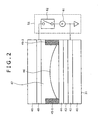
- the lower substrate 41 and the upper substrate 49 are formed by using a transparent material that allows the passage of light, such as glass or silicon.
- the rib 45-1 and the rib 45-2 are shown in FIG. 2 in such a manner as to be separated into two portions because FIG. 2 is a sectional view, they are continuous with each other and are formed as one component in practice.
- the rib 45 In addition, the part surrounded by this rib 45 will be referred to as a rib pixel. It is desired that this rib 45 does not dissolve in the polar liquid 47 and the nonpolar liquid 46 and does not react with them.
- a polymer resin is used, and e.g. an epoxy resin or an acrylic resin is used. It is obvious that another material having the characteristics similar to these resins may be used.
- the water-repellent film 44 has the insulating property as well as the hydrophobicity. Therefore, it is possible to structurally insulate the lower electrode 42 and the upper electrode 48 with only the water-repellent film 44.
- the dielectric strength of the water-repellent film 44 is low, and the film thickness thereof needs to be set large in order to keep sufficient strength.
- the film thickness is increased, the dielectric constant is lowered. Thus, the drive voltage is increased, which possibly causes increase in the power consumption and so on.
- a liquid device array 71C shown on the upper side of FIG. 5 is obtained by arranging the conventional liquid devices of this case in an array
- a liquid device array 71D shown on the lower side of FIG. 5 is obtained by arranging the liquid devices 31, to which the present invention is applied, of this case in an array.
- the white circles ( ⁇ ) indicate the relationship between the breakdown amplitude voltage and the water-repellent film thickness when the insulating film 43 is not provided but only the water-repellent film 44 is provided like in the configuration of the conventional liquid device.
- the black circles ( ⁇ ) indicate the relationship between the breakdown amplitude voltage and the water-repellent film thickness when the film thickness of the insulating film 43 composed of an inorganic material is 100 nm.
- the black squares ( ⁇ ) indicate the relationship between the breakdown amplitude voltage and the water-repellent film thickness when the film thickness of the insulating film 43 composed of an inorganic material is 50 nm.
- the lower electrodes 42 plural ITO electrodes were disposed in a line manner on the lower substrate 41 with a film thickness of 30 nm, an electrode width of 30 ⁇ m, and an electrode interval of 5 ⁇ m.
- the electrode thus disposed in a line manner will be referred to as the line electrode.
- the white squares ( ⁇ ) indicate the relationship between the breakdown amplitude voltage and the water-repellent film thickness when only the water-repellent film 44 is provided, as with the case of the white circles.
- the phases of the applied rectangular wave are shifted from each other by 180 degrees between adjacent line electrodes. That is, in this case, the potential difference twice the amplitude voltage arises between the line electrodes.
- the breakdown amplitude voltage of this case indicates the potential difference between the lower electrodes 42, i.e. between the line electrodes.
- the black circles (•) indicate the relationship between the breakdown amplitude voltage and the water-repellent film thickness when the insulating film 43 that has a film thickness of 100 nm and is composed of an inorganic material is newly provided like in the liquid device 31 and the phases of the applied rectangular wave are aligned with each other between adjacent line electrodes.
- the black squares ( ⁇ ) indicate the relationship between the breakdown amplitude voltage and the water-repellent film thickness when the insulating film 43 that has a film thickness of 100 nm and is composed of an inorganic material is newly provided, as with the case of the black circles, but the phases of the applied rectangular wave are shifted from each other by 180 degrees between adjacent line electrodes.
- the breakdown strength in the first experiment for the blanket-film electrode structure should be the same as that in the present experiment for the patterning-electrode structure.
- the breakdown strength of the patterning-electrode structure in the present experiment was lower. This will be attributed to the following reason.
- the major solvent for coating the water-repellent film was an extremely-special solution containing fluorine, and the wettability was different between the ITO electrodes and the underlying glass substrate. Therefore, unevenness occurred between the small areas corresponding to the electrode interval of 5 ⁇ m and the 30 ⁇ m areas on the electrodes, and the uniform, dense water-repellent film 44 was not formed.
- FIG. 9 is a block diagram showing a major configuration example of a manufacturing apparatus for the liquid device 31.
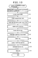
- the controller 111 has a transparent-electrode-equipped substrate fabricating section 131, a substrate cleaning section 132, an insulating film forming section 133, a water-repellent thin film forming section 134, a black matrix forming section 135, a partition forming section 136, a surface treatment section 137, an oil solution applying section 138, a purified water injecting section 139, an excess oil removing section 140, and a sealing section 141 that control the operation of the respective steps in the manufacturing of the liquid device 31 by the manufacturing unit 112.
- the transparent-electrode-equipped substrate fabricating section 131 in the controller 111 controls the manufacturing unit 112 to employ a transparent material such as glass or silicon as the lower substrate 41 and form a transparent electrode such as an ITO film as the lower electrode 42 on the lower substrate 41.
- a transparent-electrode-equipped substrate 201 that is transparent and has a predetermined size is fabricated.
- the upper substrate. 50 and the upper electrode 49 are also produced in a similar manner, and therefore the description thereof is omitted.
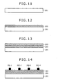
- the film thickness of the water-repellent film 203 needs to be equal to or larger than 500 nm, preferably equal to or larger than 800 nm in order to develop the desired insulating property. If a double-layered structure with the insulating film 202 and the water-repellent film 203 is employed as shown in FIG. 13 , it is sufficient that the film thickness of the water-repellent film 203 is equal to or larger than about 100 nm. Such film thickness adjustment can be achieved through adjustment of the concentration of the stock solution and the rotational speed at the time of the spin-coating.
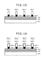
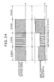
- the black matrix forming section 135 controls the manufacturing unit 112 to form a black matrix that optically separates the respective rib pixels from each other so that the incidence of extra light can be avoided. Specifically, the black matrix forming section 135 controls the manufacturing unit 112 to uniformly deposit a resist material by a spin-coating method and then perform exposure, development, and so on by a photolithography method. Thereby, for example, partitions 204-1 to 204-4 formed of a black resist containing a black pigment or dye are formed as the black matrix on the water-repellent film 203 as shown in FIG. 14 .
- the partition 204-1 and the partition 205-1 for which the surface treatment 206-1 has been performed will be referred to as a rib 207-1 collectively.
- the partition 204-2 and the partition 205-2 for which the surface treatment 206-2 has been performed will be referred to as a rib 207-2 collectively.
- the partition 204-3 and the partition 205-3 for which the surface treatment 206-3 has been performed will be referred to as a rib 207-3 collectively.
- the partition 204-4 and the partition 205-4 for which the surface treatment 206-4 has been performed will be referred to as a rib 207-4 collectively.
- the rib 207 if there is no need to make a description with distinguishing among the ribs 207-1 to 207-4, they will be referred to as the rib 207.
- Step S9 the purified water injecting section 139 controls the manufacturing unit 112 to pour purified water 209 as the polar liquid 47 into the surface of covering of the colored oil solution 208 as shown in FIG. 18 for example.
- the speed of the spreading of the purified water along the surface direction of the transparent-electrode-equipped substrate 201 is set constant by using a dispenser or the like.
- a scheme may be used in which a substrate covered by an oil is put into a water tank that is filled with the purified water 209 in advance, at a constant speed and a constant angle.
- Step S10 the excess oil removing section 140 controls the manufacturing unit 112 to remove the excess oil solution 208 floating on the surface of the purified water 209.
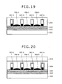
- FIG. 19 is a diagram showing the condition after the excess oil is removed.
- an adequate amount of an oil solution 208-1 forms a layer in the rib pixel between the rib 207-1 and the rib 207-2.
- An adequate amount of an oil solution 208-2 forms a layer in the rib pixel between the rib 207-2 and the rib 207-3.
- An adequate amount of an oil solution 208-3 forms a layer in the rib pixel between the rib 207-3 and the rib 207-4.
- the layer of the oil solution 208 and the layer of the purified water 209 are formed in each rib pixel.
- the nonpolar liquid 46 and the polar liquid 47 form a layer on the lower side and on the upper side, respectively, and become stable, irrespective of the specific gravities of the polar liquid 47 and the nonpolar liquid 46.
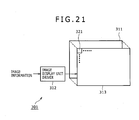
- FIG. 21 is a block diagram showing a configuration example of an image display device to which the present invention is applied.
- the image display unit 313 is a device that displays an image and in which plural liquid devices 321 that control transmission of light emitted from the light emitting source 311 under control by the image display unit driver 312 are arranged in a flat surface manner or a curved surface manner.
- This liquid device 321 is an application of the liquid device 31, to which the present invention is applied, described with reference to FIG. 2 .
- the nonpolar liquid 46 a liquid containing a black dye or a liquid colored to black through dissolving of a colorant is used.
- this colorant one that dissolves in the nonpolar liquid 46 but does not dissolve in the polar liquid 47 is used.
- a pigment that does not dissolve also in the nonpolar liquid 46 may be mixed in the nonpolar liquid 46. That is, it is sufficient that the nonpolar liquid 46 is in the state of preventing light transmission as a result while having the characteristics described with reference to FIG. 2 , and the color thereof may be one other than black.
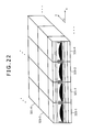
- the black nonpolar liquid 46 is pushed out and moved by the polar liquid 47 moved to the vicinity of the water-repellent film 44, and is stabilized in the state of aggregating at a part of the section surrounded by the rib 45 of the liquid device 321 as shown in FIG. 24 .
- the maximum voltage is applied.
- FIG. 25 is a diagram showing an array example of liquid devices when the liquid devices to which the present invention is applied are applied to an image display device that displays color images, and is a diagram corresponding to FIG. 22 .
- the nonpolar liquid 46 of each liquid device 321 is rendered not black but red, blue, or green.
- a nonpolar liquid 46-1 of a liquid device 321-1 and a nonpolar liquid 46-4 of a liquid device 321-4 which are indicated by a pattern of oblique lines running from the upper right to the lower left, are red.
- the nonpolar liquid 46 is transparent and allows the passage of light having a predetermined wavelength, i.e. light of the same color as that of the nonpolar liquid 46, of the light from the light emitting source 311.
- the transmitted light beams emitted from the neighboring liquid devices 321 overlap with each other. Thereby, for a user, a displayed image appears to include also colors other than red, green, and blue.
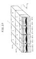
- All of the colors of the color filters 361 of the liquid devices 321 whose top surface is indicated by a character “G” are green. All of the colors of the color filters 361 of the liquid devices 321 whose top surface is indicated by a character “B” are blue. In addition, in the case of FIG. 27 , the color of the nonpolar liquids 46 of all of the liquid devices 321 is black.
- the image display device 301 is a transmissive display having the light emitting source 311 on the backside of the image display unit 313.
- it may be a display other than this, such as a reflective display.
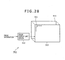
- FIG. 28 is a block diagram showing a configuration example of a reflective image display device to which the present invention is applied.
- FIG. 28 is a diagram corresponding to FIG. 21 .
- An image display device 401 shown in FIG. 28 has the image display unit driver 312 and the image display unit 313 as with the image display device 301 of FIG. 21 , but has a light reflector 411 instead of the light emitting source 311.
- the reflective image display device can be achieved in the same manner as that of the case of the transmissive image display device basically, and can display all of binary images, grayscale images, or color images.
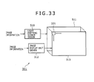
- red light, green light, and blue light are emitted with a predetermined time-division pattern from the whole of the light emitting surface of the color light emitting source 511. Therefore, red light is emitted from the whole of the light emitting surface at a certain time. Green light is emitted from the whole of the light emitting surface at another certain time, and blue light is emitted from the whole of the light emitting surface at yet another certain time.
- the description is so made that the liquid device 321 controls the light amount of transmitted light based on the degree of opening of the optical shutter.
- the light amount of transmitted light may be controlled by controlling the time period during which the optical shutter is opened.
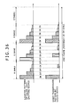
- the image display unit driver 312 adjusts the time periods of the on-state and the off-state of the switch unit 62 in an analogous manner to thereby arbitrarily control the time period during which voltage is applied to the lower electrode 42 and the upper electrode 48 of each liquid device 321 and arbitrarily control the time period of the state in which the nonpolar liquid 46 is contracted and stabilized or the time period of the state in which the nonpolar liquid 46 is expanded and stabilized. That is, in this case, the liquid device 321 is stabilized in only two states: the state in which the optical shutter is opened and the state in which it is closed. Based on the lengths of the time periods of these two stable states, the liquid device 321 controls the time period during which light passes through the rib pixel and controls the light amount of the transmitted light. In this manner, by arbitrarily controlling each of the transmission amounts of light beams of the respective colors as shown in FIG. 35 , the liquid device 321 can arbitrarily control the light amounts of the respective colors to be mixed and can make any color.
- the luminance at the time of the lighting of the respective LEDs of the color light emitting source 511 may be changed.
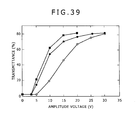
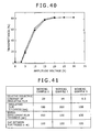
- the film thicknesses of the insulating film 43 and the water-repellent film 44 of the respective liquid devices are employed as the conditions as shown in the table of FIG. 37 , and the relationships between the amplitude voltage of the voltage applied between the lower electrode 42 and the upper electrode 48 and the transmittance of light that passes through the liquid device, i.e. the relationships between the magnitude of the applied voltage and the degree of opening of the optical shutter, under the respective conditions are compared.
- the relationships between the amplitude voltage and the transmittance at that time are shown in the graphs of FIGS. 39 and 40 .
- the white circles ( ⁇ ) indicate the relationship between the amplitude voltage and the transmittance of "Comparative example 1”
- the black circles ( ⁇ ) indicate the relationship between the amplitude voltage and the transmittance of "Working example 1”
- the black squares ( ⁇ ) indicate the relationship between the amplitude voltage and the transmittance of "Working example 2.”
- the transmittance can be sufficiently enhanced with voltages lower than the amplitude voltage with which breakdown occurs, so that the power consumption can be lowered and the reliability can be enhanced.
- the film thicknesses of the insulating film 43 and the water-repellent film 44 be decreased and the relative dielectric constants thereof be increased in theory.
- the relative dielectric constant of the substance that can be used as the insulating film 43 is at most about 20 in practice.
- decreasing the film thickness increases the possibility of the occurrence of breakdown and makes it more difficult to render the film thickness uniform without unevenness at the time of the manufacturing.
- breakdown occurs more easily at a thin part.
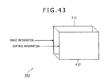
- the image display unit 611 causes light emitting pixels to emit light based on image information supplied from the external, to thereby two-dimensionally display a parallax image including parallax information.
- the parallax refers to a phenomenon that, although only one object is viewed, this object looks as images different from each other depending on the viewpoint.
- the ray reconstruction method the integral photography method (hereinafter, referred to as the IP method)
- the phenomenon that the appearance (visual image) of a three-dimensional object differs depending on the viewing angle to this object is reproduced by using many parallax images. That is, for a user viewing one parallax image that is so displayed that a parallax is generated, the image (the contents of the parallax image) appears to differ depending on the position of the user (e.g. in the horizontal direction).
- the image synthesizing method may be a method other than the above-described method as long as it matches the parallax generating method of the parallax generator 612.
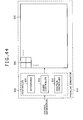
- FIG. 44 is a diagram showing a detailed configuration example of the parallax generator 612 of FIG. 43 .
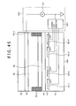
- the nonpolar liquid 46 is not colored but a colorless, transparent liquid is applied thereto. It is preferable that the polar liquid 47 and the nonpolar liquid 46 be not mixed with each other and have refractive indexes greatly different from each other, and both have low viscosity.
- the lower electrode 42 is subjected to patterning and is configured as four line electrodes from a lower electrode 42-1 to a lower electrode 42-4.
- the respective lower electrodes 42 are shown equally with a large size for convenience of description.
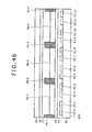
- the respective widths of the lower electrodes 42-1 to 42-4 are any, and the widths may be identical to each other or may be different from each other.
- the respective widths of the lower electrodes 42 are frequently smaller than those in the example shown in FIG. 45 compared with the length between the rib 45-1 and the rib 45-2.
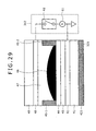
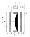
- the wettability of the polar liquid 47 to the water-repellent film 44 changes, so that the polar liquid 47 is so deformed (moved) as to aggregate around the lower electrode 42 to which the voltage is applied. Due to the deformation of the polar liquid 47, the nonpolar liquid 46 is pushed and deformed (moved). As a result, the interface between the nonpolar liquid 46 and the polar liquid 47 is deformed, which changes the optical path (the emission direction) of transmission light that passes through this liquid lens 641 upward along the vertical direction in FIG. 45 . Although the details of the operation of this liquid lens 641 will be described later, the liquid lens 641 can control the emission direction of the transmitted light based on this deformation of the interface between the nonpolar liquid 46 and the polar liquid 47.
- the liquid device 31, to which the present invention is applied can be utilized also as a liquid displacing device that displaces the position of the nonpolar liquid 46.
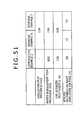
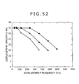
- the film thickness of the water-repellent film 44 in the liquid displacing device of "Comparative example 2" as the reference is set to 800 nm, whereas the insulating film 43 is not formed.
- the film thickness of the insulating film 43 is set to 100 nm and the film thickness of the water-repellent film 44 is set to 150 nm.
- the nonpolar liquid 46 can be displaced to a larger degree with lower potential at higher speed compared with the case of the structure with only the water-repellent film 44 like the conventional liquid device. Furthermore, the occurrence of breakdown can also be reduced.
- the liquid device 31, to which the present invention is applied can achieve increase in the capacitance and suppress breakdown in any application example. This allows the lowering of the power consumption and enhancement in the reliability.
Landscapes
- Physics & Mathematics (AREA)
- General Physics & Mathematics (AREA)
- Optics & Photonics (AREA)
- Electrochromic Elements, Electrophoresis, Or Variable Reflection Or Absorption Elements (AREA)
- Formation Of Insulating Films (AREA)
Applications Claiming Priority (3)
| Application Number | Priority Date | Filing Date | Title |
|---|---|---|---|
| JP2007002552A JP2008170631A (ja) | 2007-01-10 | 2007-01-10 | 液体デバイス、液体デバイス製造装置および方法 |
| JP2007002553A JP2008170632A (ja) | 2007-01-10 | 2007-01-10 | 液体デバイス、液体デバイス製造装置および方法 |
| PCT/JP2008/050165 WO2008084822A1 (ja) | 2007-01-10 | 2008-01-10 | 液体デバイス、液体デバイス製造装置および方法、並びに画像表示装置 |
Publications (2)
| Publication Number | Publication Date |
|---|---|
| EP2103982A1 true EP2103982A1 (de) | 2009-09-23 |
| EP2103982A4 EP2103982A4 (de) | 2012-04-11 |
Family
ID=39608710
Family Applications (1)
| Application Number | Title | Priority Date | Filing Date |
|---|---|---|---|
| EP08703036A Withdrawn EP2103982A4 (de) | 2007-01-10 | 2008-01-10 | Flüssigvorrichtung, herstellungsvorrichtung und -verfahren für flüssigvorrichtung und bildanzeigevorrichtung |
Country Status (3)
| Country | Link |
|---|---|
| US (1) | US8040583B2 (de) |
| EP (1) | EP2103982A4 (de) |
| WO (1) | WO2008084822A1 (de) |
Cited By (5)
| Publication number | Priority date | Publication date | Assignee | Title |
|---|---|---|---|---|
| EP2525246A1 (de) * | 2011-05-17 | 2012-11-21 | Japan Display East Inc. | Anzeigevorrichtung |
| EP2500771A4 (de) * | 2010-01-28 | 2013-01-23 | Sharp Kk | Anzeigeelement und elektrogerät damit |
| TWI467228B (zh) * | 2012-11-30 | 2015-01-01 | Nat Univ Chung Hsing | An electric wetting element and its making method |
| WO2019165269A1 (en) * | 2018-02-23 | 2019-08-29 | Corning Incorporated | Method of separating a liquid lens from an array of liquid lenses |
| US20220018996A1 (en) * | 2019-03-29 | 2022-01-20 | Japan Display Inc. | Lens array and display device |
Families Citing this family (21)
| Publication number | Priority date | Publication date | Assignee | Title |
|---|---|---|---|---|
| TWI396893B (zh) * | 2009-10-22 | 2013-05-21 | Univ Nat Chiao Tung | 光電裝置 |
| CN101915989B (zh) * | 2010-07-28 | 2011-12-14 | 东南大学 | 一种电场力控制的液体透镜 |
| US8693081B2 (en) * | 2010-09-30 | 2014-04-08 | University Of Cincinnati | Electrofluidic imaging film, devices, and displays, and methods of making and using the same |
| JP2013037219A (ja) * | 2011-08-09 | 2013-02-21 | Sony Corp | 光学素子、光学素子アレイ、表示装置および電子機器 |
| AU2012336040B2 (en) | 2011-11-07 | 2015-12-10 | Illumina, Inc. | Integrated sequencing apparatuses and methods of use |
| KR20130072502A (ko) * | 2011-12-22 | 2013-07-02 | 삼성디스플레이 주식회사 | 시차 배리어 패널 및 이를 포함하는 표시 장치 |
| US8982444B2 (en) * | 2012-02-09 | 2015-03-17 | Amazon Technologies, Inc. | Electrowetting display device and manufacturing method thereof |
| KR101949527B1 (ko) * | 2012-03-14 | 2019-02-18 | 리쿠아비스타 비.브이. | 전기 습윤 표시 장치 및 그 제조 방법 |
| KR101925344B1 (ko) * | 2012-05-10 | 2018-12-05 | 리쿠아비스타 비.브이. | 전기 습윤 표시장치 |
| KR101967472B1 (ko) | 2012-06-08 | 2019-04-09 | 리쿠아비스타 비.브이. | 전기습윤 표시 장치 및 이의 제조 방법 |
| CN102937744B (zh) * | 2012-10-29 | 2014-12-03 | 京东方科技集团股份有限公司 | 一种狭缝光栅及制备方法、显示装置 |
| EP2921901A4 (de) * | 2012-11-14 | 2016-04-27 | Nanobrick Co Ltd | Betrugs- und fälschungsvorbeugungsvorrichtung |
| US9594243B2 (en) * | 2013-08-20 | 2017-03-14 | Sekisui Chemical Co., Ltd. | Electrowetting device and electrowetting display |
| US9494790B1 (en) * | 2014-09-29 | 2016-11-15 | Amazon Technologies, Inc. | Electrowetting element and fluid |
| WO2017126374A1 (ja) | 2016-01-18 | 2017-07-27 | シャープ株式会社 | 電極基板およびその製造方法並びに電子機器 |
| KR20180032908A (ko) * | 2016-09-23 | 2018-04-02 | 한국과학기술원 | 전기 습윤 방식의 액체 렌즈 어레이 및 그 제조 방법과, 이를 이용한 디스플레이 장치 |
| EP3529643A1 (de) * | 2016-10-18 | 2019-08-28 | Corning Incorporated | Linse mit variablem fokus mit integriertem optischem filter und bilderfassungsvorrichtung damit |
| WO2019026812A1 (ja) | 2017-08-03 | 2019-02-07 | シャープ株式会社 | アクティブマトリクス基板、それを備えた微小流体装置およびそれらの製造方法 |
| JP2020042261A (ja) | 2018-09-06 | 2020-03-19 | シャープ株式会社 | エレクトロウェッティング装置 |
| US11217610B2 (en) | 2019-03-29 | 2022-01-04 | Sharp Kabushiki Kaisha | Method of manufacturing active matrix substrate |
| KR20220024781A (ko) | 2019-06-26 | 2022-03-03 | 코닝 인코포레이티드 | 전기습윤 광학 소자 및 그 제조방법 |
Family Cites Families (6)
| Publication number | Priority date | Publication date | Assignee | Title |
|---|---|---|---|---|
| JP4491252B2 (ja) * | 2003-01-31 | 2010-06-30 | 富士フイルム株式会社 | エレクトロウェッティング装置および表示装置 |
| FR2866493B1 (fr) | 2004-02-16 | 2010-08-20 | Commissariat Energie Atomique | Dispositif de controle du deplacement d'une goutte entre deux ou plusieurs substrats solides |
| JP4662129B2 (ja) * | 2005-03-16 | 2011-03-30 | ソニー株式会社 | 表示装置および表示制御方法 |
| JP2006285031A (ja) * | 2005-04-01 | 2006-10-19 | Sony Corp | 可変焦点レンズとこれを用いた光学装置、可変焦点レンズの製造方法 |
| JP2008203282A (ja) * | 2005-06-03 | 2008-09-04 | Sharp Corp | 画像表示装置 |
| US7697187B2 (en) * | 2006-09-29 | 2010-04-13 | Sony Corporation | Electrowetting device and varifocal lens, optical pickup device, optical recording/reproduction device, droplet operation device, optical element, zoom lens, imaging device, light modulating device, and display device using the same |
-
2008
- 2008-01-10 US US12/522,675 patent/US8040583B2/en not_active Expired - Fee Related
- 2008-01-10 EP EP08703036A patent/EP2103982A4/de not_active Withdrawn
- 2008-01-10 WO PCT/JP2008/050165 patent/WO2008084822A1/ja not_active Ceased
Cited By (10)
| Publication number | Priority date | Publication date | Assignee | Title |
|---|---|---|---|---|
| EP2500771A4 (de) * | 2010-01-28 | 2013-01-23 | Sharp Kk | Anzeigeelement und elektrogerät damit |
| EP2525246A1 (de) * | 2011-05-17 | 2012-11-21 | Japan Display East Inc. | Anzeigevorrichtung |
| CN102809811A (zh) * | 2011-05-17 | 2012-12-05 | 株式会社日本显示器东 | 显示装置 |
| US8941909B2 (en) | 2011-05-17 | 2015-01-27 | Pixtronix, Inc. | Display device |
| TWI479192B (zh) * | 2011-05-17 | 2015-04-01 | Pixtronix Inc | Display device |
| TWI467228B (zh) * | 2012-11-30 | 2015-01-01 | Nat Univ Chung Hsing | An electric wetting element and its making method |
| WO2019165269A1 (en) * | 2018-02-23 | 2019-08-29 | Corning Incorporated | Method of separating a liquid lens from an array of liquid lenses |
| US11992894B2 (en) | 2018-02-23 | 2024-05-28 | Corning Incorporated | Method of separating a liquid lens from an array of liquid lenses |
| US20220018996A1 (en) * | 2019-03-29 | 2022-01-20 | Japan Display Inc. | Lens array and display device |
| US11841515B2 (en) * | 2019-03-29 | 2023-12-12 | Japan Display Inc. | Lens array and display device |
Also Published As
| Publication number | Publication date |
|---|---|
| US8040583B2 (en) | 2011-10-18 |
| EP2103982A4 (de) | 2012-04-11 |
| US20100053717A1 (en) | 2010-03-04 |
| WO2008084822A1 (ja) | 2008-07-17 |
Similar Documents
| Publication | Publication Date | Title |
|---|---|---|
| US8040583B2 (en) | Liquid device, liquid device manufacturing apparatus and method, and image display device | |
| JP2008170631A (ja) | 液体デバイス、液体デバイス製造装置および方法 | |
| US7636187B2 (en) | Optical shutter for display device, image display apparatus, and apparatus and method for manufacturing the optical shutter | |
| JP2008170632A (ja) | 液体デバイス、液体デバイス製造装置および方法 | |
| KR101041259B1 (ko) | 디스플레이 디바이스 | |
| US7872790B2 (en) | Display capable electrowetting light valve | |
| US7274416B2 (en) | Display device | |
| CN103026294B (zh) | 显示像素、显示器以及操作显示像素的方法 | |
| KR20050092786A (ko) | 디스플레이 디바이스 | |
| US9041999B2 (en) | Electrowetting device and method of manufacturing the same | |
| JP2022107681A (ja) | 3次元ディスプレイ装置 | |
| JP2008170962A (ja) | ディスプレイ用光学シャッタ、画像表示装置、ディスプレイ用光学シャッタ製造装置および方法 | |
| WO2012066970A1 (ja) | 表示素子、及びこれを用いた電気機器 | |
| HK40041152B (en) | Three-dimensional display apparatuses | |
| HK40041152A (en) | Three-dimensional display apparatuses | |
| JP2014006412A (ja) | 表示素子、及びこれを用いた電気機器 | |
| HK1107414A (en) | Display device |
Legal Events
| Date | Code | Title | Description |
|---|---|---|---|
| PUAI | Public reference made under article 153(3) epc to a published international application that has entered the european phase |
Free format text: ORIGINAL CODE: 0009012 |
|
| 17P | Request for examination filed |
Effective date: 20090707 |
|
| AK | Designated contracting states |
Kind code of ref document: A1 Designated state(s): AT BE BG CH CY CZ DE DK EE ES FI FR GB GR HR HU IE IS IT LI LT LU LV MC MT NL NO PL PT RO SE SI SK TR |
|
| DAX | Request for extension of the european patent (deleted) | ||
| RIC1 | Information provided on ipc code assigned before grant |
Ipc: G02B 3/14 20060101AFI20120301BHEP Ipc: G02B 3/00 20060101ALN20120301BHEP Ipc: G02B 26/02 20060101ALI20120301BHEP |
|
| A4 | Supplementary search report drawn up and despatched |
Effective date: 20120309 |
|
| 17Q | First examination report despatched |
Effective date: 20130404 |
|
| STAA | Information on the status of an ep patent application or granted ep patent |
Free format text: STATUS: THE APPLICATION IS DEEMED TO BE WITHDRAWN |
|
| 18D | Application deemed to be withdrawn |
Effective date: 20130815 |