EP2104023A2 - Verfahren und Vorrichtung an einer berührungsempfindlichen Vorrichtung - Google Patents
Verfahren und Vorrichtung an einer berührungsempfindlichen Vorrichtung Download PDFInfo
- Publication number
- EP2104023A2 EP2104023A2 EP09155483A EP09155483A EP2104023A2 EP 2104023 A2 EP2104023 A2 EP 2104023A2 EP 09155483 A EP09155483 A EP 09155483A EP 09155483 A EP09155483 A EP 09155483A EP 2104023 A2 EP2104023 A2 EP 2104023A2
- Authority
- EP
- European Patent Office
- Prior art keywords
- electrodes
- display
- touch
- touch sensitive
- sensitive device
- Prior art date
- Legal status (The legal status is an assumption and is not a legal conclusion. Google has not performed a legal analysis and makes no representation as to the accuracy of the status listed.)
- Ceased
Links
Images



Classifications
-
- G—PHYSICS
- G06—COMPUTING OR CALCULATING; COUNTING
- G06F—ELECTRIC DIGITAL DATA PROCESSING
- G06F3/00—Input arrangements for transferring data to be processed into a form capable of being handled by the computer; Output arrangements for transferring data from processing unit to output unit, e.g. interface arrangements
- G06F3/01—Input arrangements or combined input and output arrangements for interaction between user and computer
- G06F3/03—Arrangements for converting the position or the displacement of a member into a coded form
- G06F3/041—Digitisers, e.g. for touch screens or touch pads, characterised by the transducing means
- G06F3/0416—Control or interface arrangements specially adapted for digitisers
- G06F3/0418—Control or interface arrangements specially adapted for digitisers for error correction or compensation, e.g. based on parallax, calibration or alignment
-
- G—PHYSICS
- G06—COMPUTING OR CALCULATING; COUNTING
- G06F—ELECTRIC DIGITAL DATA PROCESSING
- G06F3/00—Input arrangements for transferring data to be processed into a form capable of being handled by the computer; Output arrangements for transferring data from processing unit to output unit, e.g. interface arrangements
- G06F3/01—Input arrangements or combined input and output arrangements for interaction between user and computer
- G06F3/03—Arrangements for converting the position or the displacement of a member into a coded form
- G06F3/041—Digitisers, e.g. for touch screens or touch pads, characterised by the transducing means
- G06F3/0416—Control or interface arrangements specially adapted for digitisers
- G06F3/04166—Details of scanning methods, e.g. sampling time, grouping of sub areas or time sharing with display driving
- G06F3/041661—Details of scanning methods, e.g. sampling time, grouping of sub areas or time sharing with display driving using detection at multiple resolutions, e.g. coarse and fine scanning; using detection within a limited area, e.g. object tracking window
-
- G—PHYSICS
- G06—COMPUTING OR CALCULATING; COUNTING
- G06F—ELECTRIC DIGITAL DATA PROCESSING
- G06F3/00—Input arrangements for transferring data to be processed into a form capable of being handled by the computer; Output arrangements for transferring data from processing unit to output unit, e.g. interface arrangements
- G06F3/01—Input arrangements or combined input and output arrangements for interaction between user and computer
- G06F3/03—Arrangements for converting the position or the displacement of a member into a coded form
- G06F3/041—Digitisers, e.g. for touch screens or touch pads, characterised by the transducing means
- G06F3/044—Digitisers, e.g. for touch screens or touch pads, characterised by the transducing means by capacitive means
- G06F3/0445—Digitisers, e.g. for touch screens or touch pads, characterised by the transducing means by capacitive means using two or more layers of sensing electrodes, e.g. using two layers of electrodes separated by a dielectric layer
Definitions
- the present invention generally relates to touch sensitive displays and more particular to a method and apparatus for increasing the resolution of a touch sensitive display in respect of determining the point of contact of a detected touch.
- Touch sensitive devices are widely used in electronic equipment in order to facilitate the input of information from a user of the electronic equipment to an application running on the electronic equipment.
- touch sensitive displays is almost customary in the field of handheld devices such as mobile telephones and personal digital assistants (PDA:s), but the use of touch sensitive displays as input/output device in control rooms in industry applications is also steadily increasing.
- LCD Liquid Crystal Display
- other display technologies are evolving and different solutions are provided in the art for providing also these new display technologies with touch sensitivity.
- touch sensitivity For the sake of clarity will the disclosure below focus on the application of touch sensitivity on an LCD, but it is emphasized that the inventive concept disclosed below is applicable on any form of display irrespective of design technology, such as variants of the LCD, e.g.
- TFT Thin Film Transistor Displays
- PDP Plasma Display Panels
- VFD Vacuum Fluorescent Displays
- FLC Ferroelectric Liquid Crystal displays
- SSCT Surface-stabilized Cholesteric Texture-type
- OLED Organic Light-Emitting Diode
- LCOS Liquid Crystal on Silicon
- touch sensitive layer which is placed on top of the display.
- the touch sensitive layer is normally in form of two flexible superimposed plastic sheets that are separated a small distance by means of insulating spacers.
- a matrix-like pattern of electrical conductors are arranged, which pattern establishes an electric contact between the sheets at the location where the touch sensitive layer is depressed.
- a control unit scanning the matrix-like pattern on the plastic sheets may then detect the electric contact between the sheets and determine the coordinates for the depression on the display.
- Another approach for providing a touch sensitive display is to provide a display which detects a touch on the display not by means detecting an electric contact between conductors as with the solution disclosed above, but by using capacitive properties of the display.
- a capacitive coupling from the display to the object (normally a finger or a stylus) touching the display makes it possible to detect a touch on the display as well as determine the position of the touch.
- the resolution of the display in respect of determining the position of a touch on the display depends on the arrangement of the electrodes used for sensing the touch.
- An arrangement in which the electrodes are closely spaced will provide a higher resolution than a corresponding arrangement where the electrodes are spaced further apart.
- the cost for developing and manufacturing a touch sensitive display increases as the resolution of the display increases. Firstly, the technique used for disposing the electrodes on the substrate becomes more complex as the size of the electrodes and the distance between them decreases. Secondly, as the number of electrodes increases the electrical wiring and the decoding electronics needed for scanning the electrodes on the display become more complex.
- an objective of the invention is to provide a method and apparatus for increasing the resolution of a touch sensitive display by measuring properties of an electrical connection between the touch sensitive display and an object in the vicinity of the display.
- properties of the electrical connection between an electrode on the display and the object located in the vicinity of the display it is possible to determine the distance between the object and the electrode.
- the position of a touch on display may be determined.
- the electrodes used for detecting a touch may be arranged on a separate layer or may be part of the electrodes used for presenting display data on the display.
- the electrodes used for presenting display data may take any form and be arranged without consideration of the touch sensitive layer.
- the touch sensitive layer may hence be optimized for detecting a touch and be arranged based on specific needs, such as size and form of the object used for touching the screen (e.g. a finger, pen, stylus etc.).
- An advantage of using the electrodes on the internal layers of the display for sensing a touch i.e. the electrodes used for presenting display data
- the need for an extra layer is removed.
- the brightness of the display may hence be increased.
- Fig. 1a illustrates a display 1 on which electrodes 2 are arranged as pixels 3 in a matrix 4.
- the dotted lines in the figure indicate that the matrix 4 may be of an arbitrary size depending on the required resolution and/or by the size of the display 1. As mentioned above a higher density of pixels will provide a higher resolution on the display 1.
- the pixel 3 arrangement illustrated in Fig. 1 it is possible to produce text or images on the display 1 by activating selected pixels 3 such that they together form the desired text or image.
- the electrodes 2 illustrated in figure 1a are square shaped, but any other shape, such as circular or triangular shapes as shown in figures 1b and 1c , respectively, or other more complex shapes, such as characters, numbers, figures etc are equally possible depending on the specific application of the display 1.
- Fig. 2 illustrates an alternative electrode 2 arrangement know as a seven-segment display 1.
- the technology used for creating the segments i.e. electrodes 2) may be the same as in Figs 1a-c .
- the arrangement of the electrodes 2 is such that by proper activation of the pixels 3, digits may be formed on the display 1.
- the arrangement of pixels 3 on the display 1 may be in any form depending on the specific requirements put on the display 1.
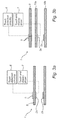
- the implementation of the touch sensitivity of the display 1 will not affect the operation of the display 1 in respect of displaying data by means of the electrodes 2a, 2b on the internal layers.
- the electrodes 5 on the touch sensitive layer will use its own wiring and dedicated electronic circuitry 6 for detecting the touch.
- the implementation of the touch sensitivity of the display 1 requires the touch detecting circuitry 7 to interact with the electronic circuitry used for presenting data on the display 1.
- the extra touch electrodes 5 may be omitted since the touch is detected by means of electrodes 2a and/or 2b.
- the touch detecting circuitry 6,7 may either be integral with or separate from the circuitry used for presenting data 7.
- the touch electrodes 5 may be disposed on the same substrate 8 as the front electrode 2a of the display 1.
- the touch electrodes 5 may then be covered with a protective coating (not shown) in order to extend the endurance of the touch sensitive display 1.
- the touch electrodes 5 may be disposed on a separate substrate 9 which is arranged in front of the substrates 10a, 10b carrying the display electrodes 2a, 2b.
- the touch electrodes 5 may either be arranged on the top or bottom surface of the substrate 9. In the latter case, no protective coating is needed in order to protect the touch electrodes 5 from wear by repeated touches since the substrate itself will protect the electrodes 5. However, a thin protective coating may still be needed in order to prevent oxidation of the electrodes 5.
- the touch electrodes 5 be arranged both on the top and bottom surface of the substrate 9.
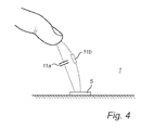
- Fig. 4 is an enlarged illustration of a touch electrode 5 in the vicinity of a finger.
- the finger or any other suitable object such as an stylus, approaches the electrode 5, an electrical connection will be established between the finger and the electrode 5.
- this electrical connection is illustrated by means of a capacitance 11a and a resistance 11b. The closer the finger gets to the display the greater the electrical connection will become. I.e. if the finger is located a certain distance x from the electrode 5 the electrical discharge rate from the electrode 5 to the finger will assume a certain value. If the distance x decreases the discharge rate from the electrode to the finger will increase. By measuring the discharge rate from the electrode 5 to the finger it is hence possible to determine the distance x.
- the environment in which the electrode 5 is situated may affect the discharge rate from the electrode 5. It is however possible to compensate for any changes in the environment and correctly determine the distance x by e.g. measuring the rate of change of the discharge rate or by calibrating the display in quiescent state. It is also possible to continuously calibrate the display by e.g. determining a moving average reflecting the environment in which a touch is to be detected.
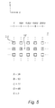
- Fig. 5 illustrates a first embodiment of the present invention for increasing the resolution of the touch sensitive display.
- the pixels 3 illustrated in Fig. 5 represent a portion of a touch sensitive display 1 comprising more pixels 3 as indicated by the dotted lines. However, it is equally possible that the touch sensitive display 1 comprises fewer pixels 3 than shown in the figure.
- the read-out from the pixel 3 (electrode 2) denoted “A” in Fig. 5 is "36".
- This value may, as disclosed in relation to Fig. 4 above, correspond to the discharge rate of the electrode 5 or to a potential measured at the electrode 5 due to an object present in the vicinity of the electrode 5.
- the read-out from the pixel denoted “B” is "93"
- from "C” is "77”
- D is "66”
- E" is "0".
- Fig. 6 illustrates a second embodiment of the present invention for increasing the resolution of the touch sensitive display 1.
- the touch sensitive display 1 may comprise more electrodes.
- the read-out values of the electrodes 61a, 61b, 61c, respectively are determined in accordance with the above disclosure in relation to Fig. 4 . These values correspond to the distances r1, r2 and r3, respectively, shown in Fig. 6 .
- r1, r2 and r3 it is possible to determine the x and y position of the touch 62 with high accuracy. More specifically, according to the present invention it is possible to determine the position of the touch 62 based on the read-outs from the electrodes 61a, 61b and 61c and not only on their actual positions. The higher the accuracy of the read-out that is provided, the higher the resolution of the touch sensitive display becomes. From a geometrical point of view it is only the actual positions of the electrodes 61a, 61b and 61c that need to be determined in order to provide a touch sensitive display that has a resolution that is substantially higher than spacing between the actual electrodes 61a, 61b and 61c.
- a "touch potentiometer” i.e. the display 1 may present a button which may not only take the values “on” or “off”, but which may act as a potentiometer which value depends on the distance between the touch-sensitive display and the object, e.g. a finger, used for pointing at the display 1.
- a look-up table may be provided which comprises data for determining the position of the touch. More specifically, the LUT may comprise measuring data for a number of points which give the position of the touch by a simple read-out from the LUT.
- the read-outs from the electrodes 3 "A" to "E", i.e. 36, 93, 77, 66 and 0 give an address in the LUT which returns the value of the position of the touch based on an earlier measurement.
- the LUT will become very large in order to provide the required resolution of the touch sensitive display.
- the LUT by collecting the electrodes into blocks and performing measurements on each block one by one it is possible to keep the LUT smaller by simply adding an offset to the determined position based on the position of the block of electrodes on the display.
- a finger will normally provide a specific target image. In a two-dimensional projection this image will be substantial circular-shaped due to the shape of the finger tip. The read-outs from the electrodes in the center of the substantial circular target image will be higher than from the electrodes at the perimeter of the target image.
- the amplitudes of the read-out from the electrodes 5 will assume a bell-shaped figure when measuring from the perimeter of the target image through the centre and out to the opposite perimeter.
- a further embodiment may use a specific object, or stylus, carrying a specified touch signature, i.e. the shape of the target image is well defined and known in advance.
- the shape of the object used for touching the display 1 may hence provide e.g. a target image rising in steps making it possible to very accurately determine the position of the touch.
- an object with a target image rising in steps may be used by a system administrator of a system using the touch sensitive display 1 in order to provide access to specific menus used for configuring the system.
- An "ordinary" user of the system who uses the fingertip for touching the display 1 may then be prevented from accessing the configuration menus.
- An alternative embodiment of the method shown in Fig. 6 is to initially use three or more electrodes 5 on the display 1 for detecting a touch on the display 1.
- the electrodes 5 may be located in the centre of the display 1 and when a touch is detected and the coordinates of the touch are determined a second measurement is performed using a second set of electrodes located in the vicinity of the initially determined coordinates. Since the distance between the actual touch and the initially determined coordinates will most likely be smaller, the second measurement will provide a more accurately determined position of the touch on the display 1. This is due to the fact that the precision of the measurement increases as the distance between the actual touch and the electrodes used for the measurement decreases.
- the detection method may continue using a third set of electrodes closer to the touch determined using the second set of electrodes. This iterative method may continue a predetermined number of times or until the distance between two consecutive sets of electrodes is below a predetermined threshold.
- the position of the touch may initially be determined by a number of iterations using the method shown in Fig. 6 whereafter a final position of the touch is determined using a LUT as disclosed above.
- the size of the LUT may then be kept small due to the reduced size of the area or block being scanned
Landscapes
- Engineering & Computer Science (AREA)
- General Engineering & Computer Science (AREA)
- Theoretical Computer Science (AREA)
- Human Computer Interaction (AREA)
- Physics & Mathematics (AREA)
- General Physics & Mathematics (AREA)
- Measurement Of Length, Angles, Or The Like Using Electric Or Magnetic Means (AREA)
- Position Input By Displaying (AREA)
Applications Claiming Priority (1)
| Application Number | Priority Date | Filing Date | Title |
|---|---|---|---|
| SE0800626 | 2008-03-18 |
Publications (2)
| Publication Number | Publication Date |
|---|---|
| EP2104023A2 true EP2104023A2 (de) | 2009-09-23 |
| EP2104023A3 EP2104023A3 (de) | 2012-08-22 |
Family
ID=40756347
Family Applications (1)
| Application Number | Title | Priority Date | Filing Date |
|---|---|---|---|
| EP09155483A Ceased EP2104023A3 (de) | 2008-03-18 | 2009-03-18 | Verfahren und Vorrichtung an einer berührungsempfindlichen Vorrichtung |
Country Status (1)
| Country | Link |
|---|---|
| EP (1) | EP2104023A3 (de) |
Cited By (20)
| Publication number | Priority date | Publication date | Assignee | Title |
|---|---|---|---|---|
| EP2562623A1 (de) * | 2011-08-21 | 2013-02-27 | TPK Touch Solutions (Xiamen) Inc. | Berührungsempfindliche Verfahren und Vorrichtungen dafür |
| CN102955601A (zh) * | 2011-08-25 | 2013-03-06 | 丽智科技股份有限公司 | 触控面板的3d感测方法及系统 |
| US8418046B2 (en) | 2008-02-13 | 2013-04-09 | Apple Inc. | Data signal handling circuitry and methods with error analysis capabilities |
| US20140075379A1 (en) * | 2012-09-11 | 2014-03-13 | Erich Schlaepfer | Direct character display control |
| EP2521015A4 (de) * | 2009-10-09 | 2014-06-18 | Egalax Empia Technology Inc | Verfahren und vorrichtung zur positionserkennung |
| WO2015048583A1 (en) | 2013-09-27 | 2015-04-02 | Sensel, Inc. | Touch sensor detector systems and method |
| US9377894B2 (en) | 2014-05-22 | 2016-06-28 | Sony Corporation | Selective turning off/dimming of touch screen display region |
| US9442597B2 (en) | 2012-10-19 | 2016-09-13 | Apple Inc. | Sensor-based ESD detection |
| US9569025B2 (en) | 2014-04-16 | 2017-02-14 | Microchip Technology Incorporated | LCD controller with capacitive touch interface |
| US9625997B2 (en) | 2013-07-19 | 2017-04-18 | Microchip Technology Incorporated | Human interface device and method |
| EP3049901A4 (de) * | 2013-09-27 | 2017-06-07 | Sensel, Inc. | System und verfahren mit einem resistiven berührungsempfindlichen sensor |
| US9689906B2 (en) | 2009-10-09 | 2017-06-27 | Egalax_Empia Technology Inc. | Method and device for position detection |
| US9811204B2 (en) | 2014-06-23 | 2017-11-07 | Apple Inc. | Time multiplexed touch detection and power charging |
| EP3161591A4 (de) * | 2014-06-25 | 2017-11-15 | Sensel, Inc. | System und verfahren mit taktilem berührungssensor |
| US9927933B2 (en) | 2014-07-10 | 2018-03-27 | Microchip Technology Germany Gmbh | Method and system for gesture detection and touch detection |
| EP2972571B1 (de) * | 2013-03-14 | 2018-08-22 | Microchip Technology Incorporated | Kapazitives gesteneingabesystem |
| US10061459B2 (en) | 2009-10-09 | 2018-08-28 | Egalax_Empia Technology Inc. | Method and device for position detection |
| US10338722B2 (en) | 2013-09-27 | 2019-07-02 | Sensel, Inc. | Tactile touch sensor system and method |
| US11221706B2 (en) | 2013-09-27 | 2022-01-11 | Sensel, Inc. | Tactile touch sensor system and method |
| WO2022217624A1 (zh) * | 2021-04-12 | 2022-10-20 | 武汉华星光电半导体显示技术有限公司 | 触控显示面板及显示装置 |
Citations (1)
| Publication number | Priority date | Publication date | Assignee | Title |
|---|---|---|---|---|
| WO2005114369A2 (en) * | 2004-05-06 | 2005-12-01 | Apple Computer, Inc. | Multipoint touchscreen |
Family Cites Families (6)
| Publication number | Priority date | Publication date | Assignee | Title |
|---|---|---|---|---|
| DE3910977A1 (de) * | 1989-04-05 | 1990-10-11 | Harms & Wende Gmbh U Co Kg | Komputereingabevorrichtung |
| US5210380A (en) * | 1990-04-06 | 1993-05-11 | Summagraphics Corporation | Digitizer with serpentine-type conductor grid having uniform conductor repeat increments |
| GB9406702D0 (en) * | 1994-04-05 | 1994-05-25 | Binstead Ronald P | Multiple input proximity detector and touchpad system |
| US7683890B2 (en) * | 2005-04-28 | 2010-03-23 | 3M Innovative Properties Company | Touch location determination using bending mode sensors and multiple detection techniques |
| GB2428306B (en) * | 2005-07-08 | 2007-09-26 | Harald Philipp | Two-dimensional capacitive position sensor |
| DE102006013937A1 (de) * | 2006-03-16 | 2007-09-27 | Prettl Appliance Systems Gmbh | Bedienblendenanordnung für Haushaltsmaschinen und Verfahren zur Herstellung einer Bedienblendenanordnung |
-
2009
- 2009-03-18 EP EP09155483A patent/EP2104023A3/de not_active Ceased
Patent Citations (1)
| Publication number | Priority date | Publication date | Assignee | Title |
|---|---|---|---|---|
| WO2005114369A2 (en) * | 2004-05-06 | 2005-12-01 | Apple Computer, Inc. | Multipoint touchscreen |
Cited By (37)
| Publication number | Priority date | Publication date | Assignee | Title |
|---|---|---|---|---|
| US8418046B2 (en) | 2008-02-13 | 2013-04-09 | Apple Inc. | Data signal handling circuitry and methods with error analysis capabilities |
| US10061459B2 (en) | 2009-10-09 | 2018-08-28 | Egalax_Empia Technology Inc. | Method and device for position detection |
| US9689906B2 (en) | 2009-10-09 | 2017-06-27 | Egalax_Empia Technology Inc. | Method and device for position detection |
| EP2521015A4 (de) * | 2009-10-09 | 2014-06-18 | Egalax Empia Technology Inc | Verfahren und vorrichtung zur positionserkennung |
| EP2562623A1 (de) * | 2011-08-21 | 2013-02-27 | TPK Touch Solutions (Xiamen) Inc. | Berührungsempfindliche Verfahren und Vorrichtungen dafür |
| CN102955601A (zh) * | 2011-08-25 | 2013-03-06 | 丽智科技股份有限公司 | 触控面板的3d感测方法及系统 |
| CN102955601B (zh) * | 2011-08-25 | 2015-09-16 | 丽智科技股份有限公司 | 触控面板的3d感测方法及系统 |
| US20140075379A1 (en) * | 2012-09-11 | 2014-03-13 | Erich Schlaepfer | Direct character display control |
| US9442597B2 (en) | 2012-10-19 | 2016-09-13 | Apple Inc. | Sensor-based ESD detection |
| US9703422B2 (en) | 2012-10-19 | 2017-07-11 | Apple Inc. | Sensor-based ESD detection |
| US10474298B2 (en) | 2013-03-14 | 2019-11-12 | Microchip Technology Incorporated | Capacitive based gesture input system |
| EP2972571B1 (de) * | 2013-03-14 | 2018-08-22 | Microchip Technology Incorporated | Kapazitives gesteneingabesystem |
| US10365722B2 (en) | 2013-07-19 | 2019-07-30 | Microchip Technology Germany Gmbh | Human interface device and method |
| US9625997B2 (en) | 2013-07-19 | 2017-04-18 | Microchip Technology Incorporated | Human interface device and method |
| US9958953B2 (en) | 2013-07-19 | 2018-05-01 | Microchip Technology Germany Gmbh | Human interface device and method |
| WO2015048584A1 (en) | 2013-09-27 | 2015-04-02 | Sensel , Inc. | Capacitive touch sensor system and method |
| US10338722B2 (en) | 2013-09-27 | 2019-07-02 | Sensel, Inc. | Tactile touch sensor system and method |
| EP3049902A4 (de) * | 2013-09-27 | 2017-06-07 | Sensel, Inc. | Kapazitives berührungssensorsystem und verfahren |
| US11809672B2 (en) | 2013-09-27 | 2023-11-07 | Sensel, Inc. | Touch sensor detector system and method |
| US11650687B2 (en) | 2013-09-27 | 2023-05-16 | Sensel, Inc. | Tactile touch sensor system and method |
| US11520454B2 (en) | 2013-09-27 | 2022-12-06 | Sensel, Inc. | Touch sensor detector system and method |
| EP3049901A4 (de) * | 2013-09-27 | 2017-06-07 | Sensel, Inc. | System und verfahren mit einem resistiven berührungsempfindlichen sensor |
| US11068118B2 (en) | 2013-09-27 | 2021-07-20 | Sensel, Inc. | Touch sensor detector system and method |
| US11221706B2 (en) | 2013-09-27 | 2022-01-11 | Sensel, Inc. | Tactile touch sensor system and method |
| US10073565B2 (en) | 2013-09-27 | 2018-09-11 | Sensel, Inc. | Touch sensor detector system and method |
| EP3049900A4 (de) * | 2013-09-27 | 2017-06-07 | Sensel, Inc. | Berührungssensor-detektorsysteme und verfahren |
| WO2015048582A1 (en) | 2013-09-27 | 2015-04-02 | Sensel, Inc. | Resistive touch sensor system and method |
| WO2015048583A1 (en) | 2013-09-27 | 2015-04-02 | Sensel, Inc. | Touch sensor detector systems and method |
| US10534478B2 (en) | 2013-09-27 | 2020-01-14 | Sensel, Inc. | Touch sensor detector system and method |
| US10705643B2 (en) | 2013-09-27 | 2020-07-07 | Sensel, Inc. | Tactile touch sensor system and method |
| US9569025B2 (en) | 2014-04-16 | 2017-02-14 | Microchip Technology Incorporated | LCD controller with capacitive touch interface |
| US9377894B2 (en) | 2014-05-22 | 2016-06-28 | Sony Corporation | Selective turning off/dimming of touch screen display region |
| US9811204B2 (en) | 2014-06-23 | 2017-11-07 | Apple Inc. | Time multiplexed touch detection and power charging |
| EP3161591A4 (de) * | 2014-06-25 | 2017-11-15 | Sensel, Inc. | System und verfahren mit taktilem berührungssensor |
| US9927933B2 (en) | 2014-07-10 | 2018-03-27 | Microchip Technology Germany Gmbh | Method and system for gesture detection and touch detection |
| WO2022217624A1 (zh) * | 2021-04-12 | 2022-10-20 | 武汉华星光电半导体显示技术有限公司 | 触控显示面板及显示装置 |
| US11914826B2 (en) | 2021-04-12 | 2024-02-27 | Wuhan China Star Optoelectronics Semiconductor Display Technology Co., Ltd. | Touch display panel and display device |
Also Published As
| Publication number | Publication date |
|---|---|
| EP2104023A3 (de) | 2012-08-22 |
Similar Documents
| Publication | Publication Date | Title |
|---|---|---|
| EP2104023A2 (de) | Verfahren und Vorrichtung an einer berührungsempfindlichen Vorrichtung | |
| US10067590B2 (en) | Differential force and touch sensing | |
| EP3040828B1 (de) | Berührungsbildschirm und anzeigevorrichtung damit | |
| US8531431B2 (en) | High speed 3D multi touch sensitive device | |
| US8125454B2 (en) | Resistive type touch panel | |
| US20140362045A1 (en) | Input interface, handheld electronic device and method of producing an input interface | |
| CN108012557B (zh) | 利用专用力接收器电极使用跨电容来感测力 | |
| KR20100036850A (ko) | 접촉 감지 센서를 이용한 터치 패널 장치 | |
| JP2010507166A (ja) | 電子装置及びそのタッチパネル配置方法 | |
| US20120280945A1 (en) | Touch display device | |
| TW201512737A (zh) | 具有整合式觸控螢幕的顯示裝置 | |
| CN102289316A (zh) | 用于在触摸系统中校正触摸坐标的方法和装置 | |
| JP6932646B2 (ja) | フォース検出機能を備える一体型表示装置及び検出装置 | |
| CN102282534A (zh) | 输入装置 | |
| US20140176498A1 (en) | Touch sensor device, electronic apparatus, position calculation method, and position calculation program | |
| US20110273395A1 (en) | Touch screen and method for controlling the same | |
| JP2005522791A (ja) | タッチセンシティブ表示装置 | |
| US20100315361A1 (en) | Touch-point coordinate detecting method | |
| TW201516774A (zh) | 觸摸點及觸摸壓力的檢測方法 | |
| JP2011048541A (ja) | タッチパネル付き表示装置 | |
| JP2012022664A (ja) | タッチパネルの圧力センシングモジュール及びその作動方法 | |
| US9323388B2 (en) | Touch panel system, and electronic information device | |
| CN109791447B (zh) | 触摸感测设备、触控显示面板、触控显示设备和触摸感测方法 | |
| US20150029138A1 (en) | Method of recognizing touch | |
| CN107239173B (zh) | 触控装置、触控显示装置及其驱动方法 |
Legal Events
| Date | Code | Title | Description |
|---|---|---|---|
| PUAI | Public reference made under article 153(3) epc to a published international application that has entered the european phase |
Free format text: ORIGINAL CODE: 0009012 |
|
| AK | Designated contracting states |
Kind code of ref document: A2 Designated state(s): AT BE BG CH CY CZ DE DK EE ES FI FR GB GR HR HU IE IS IT LI LT LU LV MC MK MT NL NO PL PT RO SE SI SK TR |
|
| AX | Request for extension of the european patent |
Extension state: AL BA RS |
|
| PUAL | Search report despatched |
Free format text: ORIGINAL CODE: 0009013 |
|
| AK | Designated contracting states |
Kind code of ref document: A3 Designated state(s): AT BE BG CH CY CZ DE DK EE ES FI FR GB GR HR HU IE IS IT LI LT LU LV MC MK MT NL NO PL PT RO SE SI SK TR |
|
| AX | Request for extension of the european patent |
Extension state: AL BA RS |
|
| RIC1 | Information provided on ipc code assigned before grant |
Ipc: G06F 3/041 20060101AFI20120713BHEP Ipc: G06F 3/044 20060101ALI20120713BHEP |
|
| AKY | No designation fees paid | ||
| REG | Reference to a national code |
Ref country code: DE Ref legal event code: R108 Effective date: 20130502 |
|
| 17P | Request for examination filed |
Effective date: 20130603 |
|
| RBV | Designated contracting states (corrected) |
Designated state(s): AT BE BG CH CY LI |
|
| RBV | Designated contracting states (corrected) |
Designated state(s): AT BE BG CH CY CZ DE DK EE ES FI FR GB GR HR HU IE IS IT LI LT LU LV MC MK MT NL NO PL PT RO SE SI SK TR |
|
| RAP1 | Party data changed (applicant data changed or rights of an application transferred) |
Owner name: SWEDIN, ANDERS |
|
| RIN1 | Information on inventor provided before grant (corrected) |
Inventor name: SWEDIN, ANDERS |
|
| 17Q | First examination report despatched |
Effective date: 20160222 |
|
| STAA | Information on the status of an ep patent application or granted ep patent |
Free format text: STATUS: THE APPLICATION HAS BEEN REFUSED |
|
| 18R | Application refused |
Effective date: 20170519 |