EP2104141B1 - Structure de feuille et procédé de fabrication associée - Google Patents
Structure de feuille et procédé de fabrication associée Download PDFInfo
- Publication number
- EP2104141B1 EP2104141B1 EP09155530.0A EP09155530A EP2104141B1 EP 2104141 B1 EP2104141 B1 EP 2104141B1 EP 09155530 A EP09155530 A EP 09155530A EP 2104141 B1 EP2104141 B1 EP 2104141B1
- Authority
- EP
- European Patent Office
- Prior art keywords
- carbon nanotube
- coating film
- linear structures
- sheet
- carbon nanotubes
- Prior art date
- Legal status (The legal status is an assumption and is not a legal conclusion. Google has not performed a legal analysis and makes no representation as to the accuracy of the status listed.)
- Active
Links
Images








Classifications
-
- H—ELECTRICITY
- H10—SEMICONDUCTOR DEVICES; ELECTRIC SOLID-STATE DEVICES NOT OTHERWISE PROVIDED FOR
- H10W—GENERIC PACKAGES, INTERCONNECTIONS, CONNECTORS OR OTHER CONSTRUCTIONAL DETAILS OF DEVICES COVERED BY CLASS H10
- H10W40/00—Arrangements for thermal protection or thermal control
- H10W40/70—Fillings or auxiliary members in containers or in encapsulations for thermal protection or control
- H10W40/77—Auxiliary members characterised by their shape
-
- C—CHEMISTRY; METALLURGY
- C09—DYES; PAINTS; POLISHES; NATURAL RESINS; ADHESIVES; COMPOSITIONS NOT OTHERWISE PROVIDED FOR; APPLICATIONS OF MATERIALS NOT OTHERWISE PROVIDED FOR
- C09K—MATERIALS FOR MISCELLANEOUS APPLICATIONS, NOT PROVIDED FOR ELSEWHERE
- C09K5/00—Heat-transfer, heat-exchange or heat-storage materials, e.g. refrigerants; Materials for the production of heat or cold by chemical reactions other than by combustion
- C09K5/08—Materials not undergoing a change of physical state when used
-
- B—PERFORMING OPERATIONS; TRANSPORTING
- B82—NANOTECHNOLOGY
- B82B—NANOSTRUCTURES FORMED BY MANIPULATION OF INDIVIDUAL ATOMS, MOLECULES, OR LIMITED COLLECTIONS OF ATOMS OR MOLECULES AS DISCRETE UNITS; MANUFACTURE OR TREATMENT THEREOF
- B82B1/00—Nanostructures formed by manipulation of individual atoms or molecules, or limited collections of atoms or molecules as discrete units
-
- B—PERFORMING OPERATIONS; TRANSPORTING
- B82—NANOTECHNOLOGY
- B82B—NANOSTRUCTURES FORMED BY MANIPULATION OF INDIVIDUAL ATOMS, MOLECULES, OR LIMITED COLLECTIONS OF ATOMS OR MOLECULES AS DISCRETE UNITS; MANUFACTURE OR TREATMENT THEREOF
- B82B3/00—Manufacture or treatment of nanostructures by manipulation of individual atoms or molecules, or limited collections of atoms or molecules as discrete units
-
- H—ELECTRICITY
- H10—SEMICONDUCTOR DEVICES; ELECTRIC SOLID-STATE DEVICES NOT OTHERWISE PROVIDED FOR
- H10W—GENERIC PACKAGES, INTERCONNECTIONS, CONNECTORS OR OTHER CONSTRUCTIONAL DETAILS OF DEVICES COVERED BY CLASS H10
- H10W40/00—Arrangements for thermal protection or thermal control
- H10W40/20—Arrangements for cooling
- H10W40/25—Arrangements for cooling characterised by their materials
-
- H—ELECTRICITY
- H10—SEMICONDUCTOR DEVICES; ELECTRIC SOLID-STATE DEVICES NOT OTHERWISE PROVIDED FOR
- H10W—GENERIC PACKAGES, INTERCONNECTIONS, CONNECTORS OR OTHER CONSTRUCTIONAL DETAILS OF DEVICES COVERED BY CLASS H10
- H10W72/00—Interconnections or connectors in packages
- H10W72/30—Die-attach connectors
-
- H—ELECTRICITY
- H10—SEMICONDUCTOR DEVICES; ELECTRIC SOLID-STATE DEVICES NOT OTHERWISE PROVIDED FOR
- H10W—GENERIC PACKAGES, INTERCONNECTIONS, CONNECTORS OR OTHER CONSTRUCTIONAL DETAILS OF DEVICES COVERED BY CLASS H10
- H10W40/00—Arrangements for thermal protection or thermal control
- H10W40/20—Arrangements for cooling
- H10W40/25—Arrangements for cooling characterised by their materials
- H10W40/257—Arrangements for cooling characterised by their materials having a heterogeneous or anisotropic structure, e.g. powder or fibres in a matrix, wire mesh or porous structures
-
- H—ELECTRICITY
- H10—SEMICONDUCTOR DEVICES; ELECTRIC SOLID-STATE DEVICES NOT OTHERWISE PROVIDED FOR
- H10W—GENERIC PACKAGES, INTERCONNECTIONS, CONNECTORS OR OTHER CONSTRUCTIONAL DETAILS OF DEVICES COVERED BY CLASS H10
- H10W72/00—Interconnections or connectors in packages
- H10W72/30—Die-attach connectors
- H10W72/321—Structures or relative sizes of die-attach connectors
- H10W72/325—Die-attach connectors having a filler embedded in a matrix
-
- H—ELECTRICITY
- H10—SEMICONDUCTOR DEVICES; ELECTRIC SOLID-STATE DEVICES NOT OTHERWISE PROVIDED FOR
- H10W—GENERIC PACKAGES, INTERCONNECTIONS, CONNECTORS OR OTHER CONSTRUCTIONAL DETAILS OF DEVICES COVERED BY CLASS H10
- H10W72/00—Interconnections or connectors in packages
- H10W72/30—Die-attach connectors
- H10W72/351—Materials of die-attach connectors
-
- H—ELECTRICITY
- H10—SEMICONDUCTOR DEVICES; ELECTRIC SOLID-STATE DEVICES NOT OTHERWISE PROVIDED FOR
- H10W—GENERIC PACKAGES, INTERCONNECTIONS, CONNECTORS OR OTHER CONSTRUCTIONAL DETAILS OF DEVICES COVERED BY CLASS H10
- H10W72/00—Interconnections or connectors in packages
- H10W72/851—Dispositions of multiple connectors or interconnections
- H10W72/874—On different surfaces
- H10W72/877—Bump connectors and die-attach connectors
-
- H—ELECTRICITY
- H10—SEMICONDUCTOR DEVICES; ELECTRIC SOLID-STATE DEVICES NOT OTHERWISE PROVIDED FOR
- H10W—GENERIC PACKAGES, INTERCONNECTIONS, CONNECTORS OR OTHER CONSTRUCTIONAL DETAILS OF DEVICES COVERED BY CLASS H10
- H10W74/00—Encapsulations, e.g. protective coatings
- H10W74/10—Encapsulations, e.g. protective coatings characterised by their shape or disposition
- H10W74/15—Encapsulations, e.g. protective coatings characterised by their shape or disposition on active surfaces of flip-chip devices, e.g. underfills
-
- H—ELECTRICITY
- H10—SEMICONDUCTOR DEVICES; ELECTRIC SOLID-STATE DEVICES NOT OTHERWISE PROVIDED FOR
- H10W—GENERIC PACKAGES, INTERCONNECTIONS, CONNECTORS OR OTHER CONSTRUCTIONAL DETAILS OF DEVICES COVERED BY CLASS H10
- H10W90/00—Package configurations
- H10W90/701—Package configurations characterised by the relative positions of pads or connectors relative to package parts
- H10W90/721—Package configurations characterised by the relative positions of pads or connectors relative to package parts of bump connectors
- H10W90/724—Package configurations characterised by the relative positions of pads or connectors relative to package parts of bump connectors between a chip and a stacked insulating package substrate, interposer or RDL
-
- H—ELECTRICITY
- H10—SEMICONDUCTOR DEVICES; ELECTRIC SOLID-STATE DEVICES NOT OTHERWISE PROVIDED FOR
- H10W—GENERIC PACKAGES, INTERCONNECTIONS, CONNECTORS OR OTHER CONSTRUCTIONAL DETAILS OF DEVICES COVERED BY CLASS H10
- H10W90/00—Package configurations
- H10W90/701—Package configurations characterised by the relative positions of pads or connectors relative to package parts
- H10W90/731—Package configurations characterised by the relative positions of pads or connectors relative to package parts of die-attach connectors
- H10W90/734—Package configurations characterised by the relative positions of pads or connectors relative to package parts of die-attach connectors between a chip and a stacked insulating package substrate, interposer or RDL
-
- Y—GENERAL TAGGING OF NEW TECHNOLOGICAL DEVELOPMENTS; GENERAL TAGGING OF CROSS-SECTIONAL TECHNOLOGIES SPANNING OVER SEVERAL SECTIONS OF THE IPC; TECHNICAL SUBJECTS COVERED BY FORMER USPC CROSS-REFERENCE ART COLLECTIONS [XRACs] AND DIGESTS
- Y10—TECHNICAL SUBJECTS COVERED BY FORMER USPC
- Y10T—TECHNICAL SUBJECTS COVERED BY FORMER US CLASSIFICATION
- Y10T428/00—Stock material or miscellaneous articles
- Y10T428/30—Self-sustaining carbon mass or layer with impregnant or other layer
Definitions
- the embodiments discussed herein are related to a sheet structure and a method of manufacturing a sheet structure, more specifically, a sheet structure including linear structure of carbon atoms and a method of manufacturing the sheet structure, and an electronic device using such sheet structure and method of manufacturing the electronic device.
- the electronic parts used in the CPUs (Central Processing Units), etc. of servers, personal computers, etc. are needed to have high radiation efficiency of heat generated by semiconductor elements.
- the structure that a heat spreader made of a material of a high specific thermal conductivity, such as copper or another, is disposed over the semiconductor element with a thermal conductive sheet, such as indium sheet or another, disposed immediately above the semiconductor element interposed therebetween.
- the linear structure of carbon atoms which is typically the carbon nanotube is noted.
- the carbon nanotube not only has a very high thermal conductivity (1500 W/m ⁇ K) but also is superior in flexibility and heat resistance, and has high potential as a heat radiation material.
- thermal conductive sheets using carbon nanotubes a thermal conductive sheet including carbon nanotubes dispersed in a resin, a thermal conductive sheet including carbon nanotube bundles orientationally grown on a substrate, which are buried with a resin, etc. are proposed.
- Japanese Laid-open Patent Publication No. 2007-009213 discloses a heat conductive material comprising a plurality of carbon nanotubes having first and second ends, heat flow collectors covering the first and/or second end, and a polymeric material filling the spaces between the plurality of carbon nanotubes.
- US2006/0231946 discloses a thermal interface including an array of generally aligned carbon nanotubes joined to a surface with a metal layer.
- the array of carbon nanotubes includes a coating on the ends of the carbon nanotubes for improved wetting of the metal layer to the ends of the carbon nanotubes so that the thermal resistance at the interface between the carbon nanotube ends and the metal is reduced.
- Japanese Laid-open Patent Publication No. 2005-150362 Japanese Laid-open Patent Publication No. 2006-147801
- Japanese Laid-open Patent Publication No. 2006-303240 Japanese Laid-open Patent Publication No. 2006-303240 .
- a sheet structure comprising: a plurality of linear structures of carbon atoms; and a first coating film formed on at least one end of the plurality of linear structures, and formed of a material having a higher heat conductivity of not less than 1 W/m ⁇ K and joining the linear structures neighboring each other, a length of a region of the plurality of linear structures covered by the first coating film being not less than 100nm.
- an electronic device comprising: a heat generator; a heat radiator for radiating heat generating from the heat generator; and a sheet structure arranged between the heat generator and the heat radiator, and including: a plurality of linear structures of carbon atoms; a first coating film formed on one end of the plurality of linear structures, and formed of a material having a higher heat conductivity of not less than 1 W/m ⁇ K, a length of a region of the plurality of linear structures covered by the first coating film being not less than 100nm; and a second coating film formed on the other end of the plurality of linear structures, and formed of a material having a higher heat conductivity of not less than 1 W/m ⁇ K, a length of a region of the plurality of linear structures covered by the second coating film being not less than 100nm.
- a method of manufacturing a sheet structure comprising: forming a catalyst metal film over a first substrate; growing over the first substrate (30) a plurality of linear structures of carbon atoms with the catalyst metal film as a catalyst; forming a first coating film over one end of the plurality of linear structures to join the neighboring linear structures so that a length of a region of the plurality of linear structures covered by the first coating film is not less than 100nm; and removing the first substrate from the interface between the plurality of linear structures and the first substrate.
- a method of manufacturing an electronic device comprising: joining a heat generator, and a heat radiator for radiating heat generated from the heat generator with a sheet structure disposed therebetween, the sheet structure including a plurality of linear structures of carbon atoms, a first coating film formed over one end of the plurality of linear structures and a second coating film formed over the other end of the plurality of linear structures; and making thermal processing at a temperature higher than a melting point of a constituent material of the first coating film and second coating film to reflow the first coating film and the second coating film.
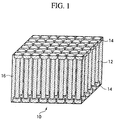
- FIG. 1 is a perspective view illustrating a structure of the carbon nanotube sheet according to the present embodiment.
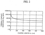
- FIG. 2 is a graph illustrating a relationship between the thermal contact resistance and the coating length of the coating film given by simulation.
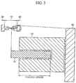
- FIG. 3 is a schematic view illustrating a condition of a heat generator and a heat radiator connected to each other via the carbon nanotube sheet.
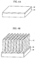
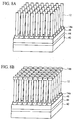
- FIGs. 4A-4B , 5A-5B , 6A-6B and 7 are perspective views illustrating a method of manufacturing the carbon nanotube sheet according to the present embodiment.
- the carbon nanotube sheet 10 has the structure that, as illustrated in FIG. 1 , a plurality of carbon nanotubes 12 having both ends coated with coating films 14 of a thermal conductive and/or electric conductive material are buried in a filling layer 16 of a resin material, a metal material or others.
- the carbon nanotubes 12 are oriented vertically to the surface of the sheet.
- the carbon nanotubes 12 may be either of single-walled carbon nanotubes or multi-walled carbon nanotubes.
- the density of the carbon nanotubes 12 is not especially limited but can be set preferably at not less than about 1 ⁇ 10 10 tubes/cm 2 from the view point of heat radiation and electric conduction.
- the length of the carbon nanotubes 12 is decided by applications of the carbon nanotube sheet 10. It is not especially limited but can be set preferably at a value of about 5 - 500 ⁇ m.
- the coating films 14 provided on the ends of the carbon nanotubes 12 are not specifically limited as long as the coating films 14 are formed of a material of high thermal conductivity. In terms of improving the thermal conductivity of the carbon nanotube sheet 10 as a whole, it is preferable to form the coating films 14 of a material of higher thermal conductivity than that of a material of the filling layer 16. In view of the thermal conductivity of about 0.1 (W/m ⁇ K) of the general resin materials, it is effective that the coating films 14 formed on both surfaces of the carbon nanotube sheet 10 are formed of a material of high thermal conductivity, e.g., not less than 1 (W/m ⁇ K).
- conductive materials e.g., metals, alloys, etc.
- materials forming the coating films 14 copper (Cu), nickel (Ni), gold (Au), indium (In), low melting point solder, etc., for example, can be used.
- the coating films 14 may not essentially have a single layer structure and may have a multilayer structure of two, three or more layers, e.g., a multilayer structure of titanium (Ti) and gold (Au).
- the contact area of the carbon nanotube sheet 10 with respect to a mounted body 8 (a heat radiator or a heat generator) can be increased in comparison with that given without the coating films 14.
- the thermal contact resistance between the carbon nanotube sheet 12 and the mounted body can be decreased, and the thermal conductivity of the carbon nanotube sheet 10. can be increased.
- the coating film 14 of a material of low melting point e.g., indium (melting point: about 157 °C) or a low melting point solder is used to thereby cause the coating films 14 to reflow after the carbon nanotube sheet 10 has been brought into contact with the mounted body.
- a material of low melting point e.g., indium (melting point: about 157 °C) or a low melting point solder
- the concavities and convexities of the contact portions between the carbon nanotube sheet 10 and the mounted body can be filled with the constituent material of the coating films 14, whereby the thermal conductivity and the electric conductivity between them can be further improved.
- FIG. 2 is a graph illustrating the relationships between the thermal contact resistance and the coating length of the coating film 14 given by simulation. On the horizontal axis, the coating length Lc of the coating film 14 is taken, and the thermal contact resistance R th is taken on the vertical axis.
- FIG. 3 is a schematic view which illustrates a heat generator 50 and a heat radiator 60 connected to each other via the carbon nanotube sheet 10.
- the carbon nanotube sheet 10 is represented by one carbon nanotube 12.
- the coating films 14 are formed covering the end regions of the carbon nanotube 12.
- the coating length Lc of the coating film 14 is a length of a region of the carbon nanotube 12 covered by the coating film 14.
- the thermal contact resistance of the carbon nanotube 12 is lower as the coating length of the coating film 14 is larger.
- the coating length Lc of the coating film 14 is not more than 100 nm, the change of the thermal contact resistance with respect to the coating length Lc is very large, and with the containing of not less than tens nm, the thermal contact resistance decreases by one placement or more.
- the coating length Lc is about three times a film thickness of the film deposited on the end surfaces of the carbon nanotubes 12.
- the gap between the carbon nanotubes 12 is about 30 - 50 nm.
- the film thickness of the coating film 12 deposited on the end surfaces of the carbon nanotubes 12 is set at not less than about 100 nm, the coating film 14 formed on the neighboring carbon nanotubes 12 comes into contact with each other, and the coating film 14 is formed continuous on the surfaces of the carbon nanotube sheet 10.
- the film thickness of the coating film 14 can be set suitably in accordance with required characteristics of the carbon nanotube sheet 10.
- the minimum film thickness of the coating film 14 can be given in terms of the thermal contact resistance described above.
- the film thickness of the coating films 14 is not less than about 30 nm (the coating length Lc is not less than about 100 nm).
- the thermal contact resistance can be improved by one placement or more in comparison with that given without the coating film 14.
- the maximum film thickness of the coating film 14 can be given in terms of a required thermal conductivity of the carbon nanotube sheet 10.
- the coating film 14 is formed of gold, whose thermal conductivity is about 300 W/m ⁇ K which is about 1/10 of the thermal conductivity of the carbon nanotubes 12, there is a risk that the coating film 14 formed too thick might decrease the thermal conductivity of the carbon nanotube sheet 10 as a whole.
- Whether the neighboring carbon nanotubes 12 are connected to each other by the coating film 14 can be selected depending on applications of the carbon nanotube sheet 10.
- each of the carbon nanotubes 12 are independent of each other, and have high flexibility. Accordingly, the flexibility of the carbon nanotubes 12 upon their contact with the mounted body can be improved.
- the transverse heat conduction and electric conduction via the coating film 14 makes it possible to use all the carbon nanotubes 12 as heat conductors, and the heat conduction can be improved.
- the surface of the coating film 14 is covered by no filling layer 16. Accordingly, when the carbon nanotube sheet 10 is in contact with a heat radiator or a heat generator, the carbon nanotubes 12 are in direct contact with the heat radiator or the heat generator, and the thermal conductive efficiency can be much improved.
- the coating film 14 is formed of an electric conductive material, whereby the carbon nanotubes 12 can be used also as interconnections passing through the sheet. That is, the carbon nanotube sheet 10 can be used not only as a heat conductive sheet, but also as a vertical interconnecting sheet. When the carbon nanotube sheet 10 is used as an interconnecting sheet, the contact resistance between the carbon nanotubes 12 and a mounted body is decreased, and the electric conductivity of the carbon nanotube sheet 10 can be increased.
- the constituent material of the filling layer 16 is not especially limited as long as the material has the property that the material is liquid when filling the spaces between the carbon nanotubes and can be hardened later.
- the organic filling materials acryl resin, epoxy resin, silicone resin, polyimide resin, etc. can be used.
- the inorganic filling materials insulating film forming compositions by using spin coating, such as SOG (Spin On Glass), etc., can be used.
- Metal materials such as indium, solder, metal pastes (e.g., silver paste), etc., can be also used.
- Conductive polymers, such as polyaniline, polythiophene, etc. can be used.
- additives may be mixed dispersed as required.
- the additives for example, substances of high thermal conductivity and substances of high electric conductivity are considered.
- Additives of high thermal conductivity are mixed dispersed in the filling layer 16 portion, whereby the thermal conductivity of the filling layer 16 portion can be improved, and the thermal conductivity of the carbon nanotube sheet 10 as a whole can be improved.
- an additive of high electric conductivity is mixed dispersed in the filling layer 16 portion, whereby the electric conductivity of the carbon nanotube sheet 10 as a whole can be improved. This is effective especially when the filling layer 16 is formed of an insulating material of low thermal conductivity, such as an organic filling material or others.
- carbon nanotubes As material of high thermal conductivity, carbon nanotubes, metal material, aluminum nitride, silica, alumina, graphite fullerene, etc. can be used. As materials of high electric conductivity, carbon nanotubes, metal materials, etc. can be used.
- a substrate 30 to be used as the base for forming the carbon nanotube sheet 10 is prepared.
- a semiconductor substrate such as a silicon substrate or others, an alumina (sapphire) substrate, an MgO substrate, a glass substrate or others can be used.
- Thin film may be formed on these substrates.
- a silicon substrate with an about 300 nm-thickness silicon oxide film formed on can be used.
- the substrate 30 is removed after the carbon nanotubes 12 have been formed. To this end, it is preferable that at least the surface of the substrate 30 is formed of a material which is easily peeled from the carbon nanotubes 12 or a material which is capable of being etched selectively with respect to the carbon nanotube sheet 10.
- a 2.5 nm-thickness Fe (iron) film is formed by, e.g., sputtering method to form a catalyst metal film 32 of Fe ( FIG. 4A ).
- the catalyst metal other than Fe, Co (cobalt), Ni (nickel), Au (gold), Ag (silver), Pt (platinum) or an alloy containing at least one of these materials may be used.
- metal particles having the size controlled in advance by a DMA (Differential Mobility Analyzer) or others may be used. In this case as well, the metal species may be the same as those of the thin film.
- film of Mo molecular metal
- Ti titanium
- Hf hafnium
- Zr zirconium
- Nb niobium
- V vanadium
- TaN tantalum nitride
- TiSi x titanium silicide
- Al aluminum
- Al 2 O 3 aluminum oxide
- TiO x titanium oxide
- Ta tantalum
- W tungsten
- Cu copper
- Au gold
- Pt platinum
- Pd palladium
- TiN titanium nitride
- an alloy containing at least one of these materials may be used.
- the layer structure of the Fe (2.5 nm)/Al (10 nm), the layer structure of Co (2.6 nm)/TiN (5 nm), etc. can be used.
- the layer structures of, e.g., Co (average diameter: 3.8 nm)/TiN (5 nm), etc. can be used.
- the carbon nanotubes are grown with the catalyst metal film 32 as the catalyst.
- the conditions for growing the carbon nanotubes are, e.g., the mixed gas of acetylene/argon (partial pressure ratio: 1:9) as the raw material gas, 1 kPa of the total gas pressure in the film forming chamber, 1000 °C of the hot filament temperature and 20 minutes of the growth period of time.
- a multi-walled carbon nanotubes of a wall number of 3 - 6 walls (about average 4 walls), a 4 - 8 nm diameter (average 6 nm) and a 80 ⁇ m-length (growth rate: 4 ⁇ m/min) can be grown.
- the carbon nanotubes may be formed by processes other than hot filament CVD method, e.g., thermal CVD method, remote plasma CVD method, etc.
- the carbon nanotubes to be grown can be single-walled carbon nanotubes.
- As the carbon raw material other than acetylene, hydrocarbons of methane, ethylene, etc. alcohols of ethanol, methanol, etc. may be used.
- a plurality of carbon nanotubes 12 oriented in the normal direction of the substrate 30 are formed ( FIG. 4B ).
- the area density of the carbon nanotubes 12 formed under the above-described growth conditions was about 1 ⁇ 10 11 tubes/cm 2 .
- a 10 nm-thickness titanium (Ti) film, for examples, and a 300 nm-thickness gold (Au) film, for example, are deposited by, e.g., sputtering method.
- Ti titanium
- Au gold
- a coating film 14a of the layer structure of Au/Ti is formed ( FIG. 5A ).
- the coating length Lc at the ends of the carbon nanotubes 12 becomes about 3 times the deposited film thickness.
- the constituent material of the coating film 14a is not especially limited as long as the material has a higher thermal conductivity than the constituent material of the filling layer 16.
- materials of electric conductivity e.g., metals, alloys, etc.
- materials of the coating film 14a copper (Cu), nickel (Ni), gold (Au), indium (In) low melting point solder, etc., for example, can be used.
- the coating film 14a may have the single structure of these metals or the layer structure of two layers or three or more layers, such as the layer structure of titanium and gold described above, etc.
- the layer structure of Au/Ti is used, because titanium is good in adhesion to the carbon nanotubes 12. Titanium film is formed between gold film and the carbon nanotubes 12, whereby the thermal contact resistance and the contact resistance between the carbon nanotubes 12 and the coating film 14a can be decreased. In terms of improving the adhesion, preferably, the titanium film is formed in a thickness of not less than about 10 nm.
- a substrate (or a sheet) 40 which is different from the substrate 30 is prepared as the substrate for the carbon nanotubes 12 formed on the substrate 30 to be transferred onto.
- a semiconductor substrate such as a silicon substrate, etc., an alumina (sapphire) substrate, an MgO substrate, a glass substrate, etc. can be used. Thin film may be formed on these substrates.
- a silicon substrate with an about 300 nm-thickness silicon oxide film formed on may be used.
- an adhesive layer 42 is formed on the substrate 40.
- the constituent material of the adhesion layer 42 a material which is capable of selectively etching the constituent material of the filling layer 16 to be formed later is used.
- the adhesion layer 42 can be formed of watersoluble polyvinyl alcohol (PVA).
- the carbon nanotubes 12 formed on the substrate 30 are transferred ( FIG. 5B ).
- the substrate 30 and the substrate 40 are bonded to each other with the surface with the coating film 14a formed on and the surface with the adhesive layer 42 formed on opposed to each other.
- the substrate 30 is peeled from the interface between the substrate 30 and the carbon nanotubes 12.
- the adhesion force of the coating film 14a with respect to the adhesive layer 42 is larger than that of the carbon nanotubes 12 with respect to the substrate 30, which allows the substrate 30 to be easily peeled form the interface with the carbon nanotubes 12.
- the carbon nanotubes 12 can be transferred onto the substrate 40.
- Ti titanium
- Au gold
- the coating film 14b of the layer structure of Au/Ti is formed over the carbon nanotubes 12 ( FIG. 6A ).
- the coating length Lc at the ends of the carbon nanotubes 12 becomes about three times the deposited film thickness.
- the constituent material of the coating film 14b is not especially limited as long as the material has a higher thermal conductivity than the constituent material of the filling layer 16.
- materials of electric conductivity e.g., metals, alloys, etc.
- materials of the coating film 14b copper (Cu), nickel (Ni), gold (Au), indium (In) low melting point solder, etc., for example, can be used.
- the coating film 14b may have the single structure of these metals or the layer structure of two layers or three or more layers, such as the layer structure of titanium and gold described above, etc.
- a filling material to be the filling layer 16 is filled between the carbon nanotubes 12.
- the substrate 40 with the carbon nanotubes 12 transferred to is pressed for, e.g., 1 minute against a substrate with silicone-based resin of an 800 mPa ⁇ s viscosity spin-coated under the conditions of, e.g., 1000 rpm and 20 seconds.
- the silicone-based resin as the filling material is filled between the carbon nanotubes 12 up to substantially the same height as the carbon nanotubes 12.
- the filling material is not especially limited as long as the filling material is liquefied and then can be solidified.
- organic fillers acryl resin, epoxy resin, silicone resin, polyimide resin, etc. can be used.
- inorganic filling materials insulating film forming compositions by using spin coating, such as SOG (Spin On Glass), etc., can be used.
- Metal materials such as indium, solder, metal pastes (e.g., silver paste), etc. can be used.
- Electric conductive polymers such as polyaniline, polythiophene, etc., can be used.
- the filling material filled between the carbon nanotubes 12 is solidified to form the filling layer 16 ( FIG. 6B ).
- the filling material can be solidified by light irradiation.
- a thermosetting material such as epoxy resin, silicone-based resin, etc.
- the filling material can be solidified by thermal processing.
- Epoxy resin can be thermally set by, e.g., 1 hour of thermal processing of 150 °C.
- Silicone-based resin can be thermally set by, e.g., 1 hour of thermal processing of 200 °C.
- the filling layer 16 on the coating film 14b may be removed by, e.g., chemical mechanical polish or oxygen plasma ashing. This is effective to remove residues of the adhesive layer 42 on the coating film 14b when they are.
- the carbon nanotubes 12 and the filling layer 16 having both ends covered by the coating film 14 are peeled from the substrate 40 to obtain the carbon nanotubes sheet 10 ( FIG. 7 ).
- the adhesive layer 42 is etched selectively with respect to the filling layer 16, whereby the carbon nanotube sheet 10 can be easily peeled.
- the adhesive layer 42 is solved by immersion in water or warm water to thereby peel the carbon nanotube sheet 10.
- the coating film of high thermal conductivity is formed on the ends of the carbon nanotubes, whereby the thermal contact resistance and the contact resistance between the carbon nanotubes and a sheet mounted body can be drastically decreased.
- the thermal conductivity, and the electric conductivity of the carbon nanotube sheet can be improved.
- FIGs. 8A to 9B The method of manufacturing the carbon nanotube sheet according to a second embodiment will be explained with reference to FIGs. 8A to 9B .
- the same members of the carbon nanotube sheet and the method of manufacturing the carbon nanotube sheet according to the first embodiment illustrated in FIGs. 1 to 7 are represented by the same reference numbers not to repeat or to simplify their explanation.
- FIGs. 8A to 9B are perspective views illustrating the method of manufacturing the carbon nanotube sheet according to the present embodiment.
- the method of manufacturing the carbon nanotube sheet according to the present embodiment is the same as the method of manufacturing the carbon nanotube sheet according to the first embodiment except the process for transferring the carbon nanotubes 12 onto the substrate 40.
- the constituent materials of the respective parts and the details of the manufacturing method are the same as those of the first embodiment.
- the carbon nanotubes 12 and the coating film 14a formed on the ends of the carbon nanotubes 12 are formed on the substrate 30.
- thermo-pressed layer 46 a layer 46 of a material which can be thermo-pressed against the coating film 14a (hereinafter called "a thermo-pressed layer 46") are formed.
- the constituent material of the thermo-pressed layer 46 gold can be used when the surface of the coating film 14a is formed of gold.
- a material which is capable of being selectively etched with respect to the thermo-pressed layer 46 is used.
- the thermo-pressed layer 46 is, e.g., gold, titanium, for example, can be used.
- the carbon nanotubes 12 formed on the substrate 30 are transferred ( FIG. 8A ).
- the substrate 30 and the substrate 40 are superimposed over each other with the surface with the coating film 14a formed on and the surface with the thermo-pressed layer 46 formed on opposed to each other.
- a pressure is applied between the substrate 30 and the substrate 40 while being heated to thereby thermo-press the coating film 14a and the thermo-pressed layer 46.
- the substrate 30 is peeled from the interface between the substrate 30 and the carbon nanotubes) 12.
- the substrate 30 can be easily peeled from the interface with the carbon nanotubes 12.
- the carbon nanotubes 12 can be transferred onto the substrate 40.
- a 10 nm-thickness titanium (Ti) film, for example, and a 50 nm-thickness gold (Au) film, for example, are deposited by, e.g., sputtering method over the carbon nanotubes 12 transferred onto the substrate 40.
- a coating film 14b of the layer structure of Au/Ti is formed over the carbon nanotubes 12 ( FIG. 8B ).
- the filling layer 16 for filling the gaps between the carbon nanotubes 12 is formed ( FIG. 9A ).
- the carbon nanotubes 12 having both ends covered by the coating films 14, and the filling layer 16 are peeled from the substrate 40, and the carbon nanotube sheet 10 is obtained ( FIG. 9B ).
- the carbon nanotube sheet 10 can be easily peeled by etching the sacrificial layer 44 selectively to the thermo-pressed layer 46.
- the thermo-pressed layer 46 is formed of gold
- the sacrificial layer 44 is formed of titanium
- the sacrificial layer 44 is dissolved by immersion into hydrofluoric acid aqueous solution to thereby peel the carbon nanotube sheet 10.
- the carbon nanotube sheet and method of manufacturing the same according to a third embodiment will be explained with reference to FIGs. 10 to 11B .
- the same members of the present embodiment as those of the carbon nanotube sheet and method of manufacturing the same according to the first and the second embodiments illustrated in FIGs. 1 to 9B are represented by the same reference numbers not to repeat or to simplify their explanation.
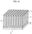
- FIG. 10 is a perspective view illustrating a structure of the carbon nanotube sheet according to the present embodiment.
- FIGs. 11A-11B are perspective views illustrating a method of manufacturing the carbon nanotube sheet according to the present embodiment.
- the carbon nanotube sheet 10 includes a graphite layer 20 between the carbon nanotubes 12 and a coating film 14.
- the graphite layer 20 is formed of graphite of a layer structure which is in parallel with the surface of the sheet and is formed, directly connected to one end of the carbon nanotubes 12.
- the thickness of the graphite layer 14 is about some nm - hundreds nm.
- the thermal conductivity of graphite is not less than above 500 times that of resin materials (thermal conductivity: about 1 W/m ⁇ K). Accordingly, the provision of the graphite layer 20 can drastically improve the heat radiation in the direction parallel with the sheet surface by not less than 500 times in comparison with that without the graphite layer 20.
- the carbon nanotube sheet 10 according to the present embodiment is formed between a heat generator and a heat radiator, the ends of the carbon nanotubes 12 on the side of the graphite layer 20 are positioned on the side of the heat generator.
- the carbon nanotube sheet 10 is so positioned, whereby the heat from the heat generator can be quickly conducted by the graphite layer 20 in the direction parallel to the sheet surface.
- the heat radiation efficiency of the heat radiation toward the heat radiator via the carbon nanotubes 12 can be improved.
- the substrate 30 is prepared as the base for forming the carbon nanotube sheet 10.
- various substrate described in the first embodiment can be used.
- the base film of the catalyst metal film 32 other than TiN, materials containing Ti, e.g., Ti (titanium), TiO 2 (titanium oxide), etc. can be used.
- the carbon nanotubes 12 having the upper surfaces covered by the graphite layer 20 are grown by, e.g., thermal CVD method ( FIG. 11A ).
- the carbon nanotubes 12 having the upper surfaces covered by the graphite layer 20 can be formed by being grown at a relatively low temperature of about 450 - 510 °C and with a hydrocarbon, e.g., acetylene, methane, ethylene, etc.-based raw material gas.
- a hydrocarbon e.g., acetylene, methane, ethylene, etc.-based raw material gas.
- a mixed gas of acetylene and argon partial pressure ratio: 1:9
- the total gas pressure in the film forming chamber is 1 kPa
- the temperature is 450 - 510 °C
- the growth period of time is 30 minutes.
- multi-walled carbon nanotubes of a wall number of 3 - 6 walls (about 4 walls at average), a 4 - 8 nm diameter (6 nm at average) and a 20 nm-lewgth can be grown.
- the graphite layer 20 of an 18 nm-thickness is also formed.
- the carbon nanotubes 12 having the upper surfaces covered by the graphite layer 20 can be formed by suitably controlling the film thickness of the catalyst metal film 32 (the film thickness of Co film) and the film forming temperature.
- the inventors of the present application made studies and have found that the carbon nanotubes 12 having the upper surfaces covered by the graphite layer 20 can be formed by being grown with the film thickness of the Co film set at 2.0 - 7.0 nm and at the film forming temperature of 350 - 560 °C.
- the thickness of the graphite layer 20 to be formed can be also controlled by the film thickness of the Co film and the film forming temperature.
- the graphite layer could be formed in a 4 nm-thickness.
- the graphite layer could be formed in an 18 nm-thickness.
- the graphite layer could be formed in a 30 nm-thickness.
- the film forming temperature set at 450 °C and the film thickness of the Co film set at 3.6 nm the graphite layer could be formed in a 20 nm-thickness.
- the growth of the carbon nanotubes 12 is made at the relatively low temperature. It is considered that in the initial growth process, the Co film of the catalyst metal film 32 has not sufficiently cohered, which permits the graphite to grow homogeneously on the catalyst metal film 32, then, together with the cohesion of the Co film, the carbon nanotubes start to grow, and consequently, the carbon nanotubes 12 having the upper surfaces covered by the graphite layer 20 are formed.
- the graphite layer 20 is formed within about 1 second of the initial growth process.
- the length of the carbon nanotubes 12 can be arbitrarily controlled by the growth period of time.
- the 10 nm-thickness titanium (Ti) film, for example, and the 50 nm-thickness gold (Au) film, for example, are deposited by, e.g., sputtering method.
- the coating film 14a of the layer structure of Au/Ti is formed over the graphite layer ( FIG. 11B ).
- the carbon nanotubes 12 are transferred onto the substrate 40, and then the coating film 14b is formed on the other ends of the carbon nanotubes 12.
- the filling layer 16 is formed between the carbon nanotubes 12, and then, the substrate 40 is peeled, and the carbon nanotube sheet 10 according to the present embodiment is completed.
- the coating film of the material of the high thermal conductivity is formed on the ends of the carbon nanotubes, whereby the thermal contact resistance and the contact resistance between the carbon nanotubes and a sheet mounted body can be drastically decreased. Because of the graphite layer directly connected to one end of the carbon nanotubes, the thermal conductivity and electric conductivity in the direction parallel to the sheet surface can be improved. Thus, the thermal conductivity and the electric conductivity of the carbon nanotube sheet can be improved.
- the carbon nanotube sheet and the method of manufacturing the same according to a fourth embodiment will be explained with reference to FIGs. 12A and 12B .
- the same members of the present embodiment as those of the carbon nanotube sheet and the method of manufacturing the same according to the first to the third embodiments illustrated in FIGs. 1 to 11B are represented by the same reference numbers not to repeat or to simplify their explanation.
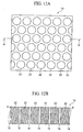
- FIG. 12A is a plan view illustrating a structure of the carbon nanotube sheet according to the present embodiment.
- FIG. 12B is a diagrammatic sectional view illustrating the structure of the carbon nanotube sheet according to the present embodiment.
- FIG. 12B is the sectional view along the line A- A' in FIG. 12A .
- the carbon nanotubes 12 are formed uniformly on the entire surface of the carbon nanotube sheet.
- the carbon nanotubes 12 may not be formed essentially on the entire surface and, as illustrated in FIG. 12 , carbon nanotube bundles 22 each containing a plurality of carbon nanotubes 12 having both ends covered by the coating film (not illustrated) may be arranged.
- the penetration of the filling material can be improved, whereby configuration changes of the carbon nanotubes 12, such as their horizontal falls, etc., can be effectively suppressed, and the initial orientation of the carbon nanotubes 12 can be easily retained.
- the gap required between the carbon nanotube bundles 22 cannot be unconditionally determined because the gap varies depending on viscosities, etc. of filling materials to be the filling layer 16.
- the gap may be sufficiently wider than a gap between the carbon nanotubes 12 forming each carbon nanotube bundle 22 and can be set at about 0.1 - 200 ⁇ m.
- the area density of the carbon nanotube in the sheet plane decreases, that is, the thermal conductivity of the sheet decreases.
- the area density of the carbon nanotubes in the sheet plane varies also depending on sizes of the carbon nanotube bundles 22. Accordingly, it is preferable to suitably set the gap between the carbon nanotube bundles 22 corresponding to the thermal conductivity required of the sheet and also in consideration of a size of the carbon nanotube bundles 22.
- each carbon nanotube bundles 22 is not limited to the circle illustrated in FIG. 12A .
- the plane shape of the carbon nanotube bundles 22 can be, other than the circle, a polygon, such as triangle, rectangle, hexagon or others.
- the arrangement of a plurality of the carbon nanotube bundles 22 is not limited to the close-packed arrangement of circles illustrated in FIG. 12A .
- the method of manufacturing the carbon nanotube sheet according to the present embodiment is the same as the first to the third embodiments except that in the present embodiment, the carbon nanotubes 12 are grown selectively on prescribed regions (regions for the carbon nanotube bundles 22 to be formed in) on the substrate 30.
- the catalyst metal film 32 may be formed selectively in the regions for the carbon nanotube bundles 22 to be formed in.
- the lift-off using a photoresist film, sputtering the catalyst metal with the surface of the substrate 30 covered with a metal mask, etc. can be used.
- the filling material spreads first along the gaps between the carbon nanotube bundles 22 and over the entire surface of the substrate 40. Then, the filling material penetrates into the carbon nanotube bundles 22.
- the filling material which has been first filled between the carbon nanotube bundles 22 plays the role of the supporter for retaining the configuration of the carbon nanotubes 12 when the filling material penetrates into the carbon nanotube bundles 22 and suppresses configuration changes of the carbon nanotube bundles 22.
- the cohesion of the carbon nanotubes 12 can be further effectively prevented.
- the coating film of a material of high thermal conductivity is formed on the ends of the carbon nanotubes, whereby the thermal contact resistance and the contact resistance between the carbon nanotubes and a sheet mounted body can be drastically decreased.
- a plurality of carbon nanotube bundles are formed, spaced from each other, whereby configuration changes of the carbon nanotube bundles can be prevented when the filing layer is formed.
- the thermal conductivity and the electric conductivity of the carbon nanotube sheet can be improved.
- the carbon nanotube sheet and the method of manufacturing the same according to a fifth embodiment will be explained with reference to FIGs. 13 to 15B .
- the same members of the present embodiment as those of the carbon nanotube sheet and the method of manufacturing the same according to the first to the fourth embodiments illustrated in FIGs. 1 to 12B are represented by the same reference numbers not to repeat or to simplify their explanation.
- FIG. 13 is a perspective view illustrating a structure of the carbon nanotube sheet according to the present embodiment.
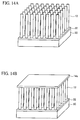
- FIGs. 14A-14B and 15A-15B are perspective views illustrating a method of manufacturing the carbon nanotube sheet according to the present embodiment.
- the carbon nanotube sheet 10 includes a plurality of carbon nanotubes 12 having both ends coated by coating films 14 of a material of thermal conductivity and/or electric conductivity.
- the coating film 14 formed on the ends of the neighboring carbon nanotubes 12 is continuous. That is, the coating film 14 is formed continuously over the entire surfaces of both surface of the carbon nanotube sheet 10.
- the carbon nanotubes 12 are oriented vertically to the surface of the sheet.
- the carbon nanotubes 12 can be either of single-walled carbon nanotubes and multi-walled carbon nanotubes.
- the density of the carbon nanotubes 12 is preferably not less than 1 ⁇ 10 10 tubes/cm 2 in terms of the heat radiation and electric conduction.
- the length of the carbon nanotubes 12 is determined by applications of the carbon nanotube sheet 10 and is not especially limited. However, the length of the carbon nanotubes 12 can be set preferably at about 5 - 500 ⁇ m.
- the material of the coating films 14 formed on both surfaces of the carbon nanotube sheet 10 is not especially limited as long as the material has a high thermal conductivity, e.g., not less than 1 (W/m ⁇ K).
- the material having a thermal conductivity of not less than 1 (W/m ⁇ K) is based on that the coating films 14 is formed of a material of a sufficiently higher thermal conductivity than the thermal conductivity of the general resin materials (about 0.1 (W/m ⁇ K)).
- the material having electric conductivity e.g., metals, alloys, etc. can be used.
- the coating film 14 may not essentially have a single layer structure and may have the layer structure of two layers or three or more layers, such as the layer structure of titanium (Ti) and gold (Au) or others.
- the contact area of the carbon nanotube sheet 10 to a mounted body can be increased.
- the thermal contact resistance of the carbon nanotubes 12 to the mounted body is decreased, and the thermal conductivity of the carbon nanotube sheet 10 can be improved.
- the gap between the carbon nanotubes 12 is about 30 - 50 nm.
- the coating films 14 to be deposited on the end surfaces of the carbon nanotubes 12 is set at above about 100 nm, the coating film 14 formed on the neighboring carbon nanotubes 12 joins each other, and the coating film 14 is formed on the surfaces of the carbon nanotube sheets 10 continuous.
- the neighboring carbon nanotubes 12 are connected to each other by the coating films 14, whereby even if the length of the carbon nanotubes 12 becomes disuniform, and resultantly some of the carbon nanotubes 12 are not in contact with a mounted body, because of the transverse thermal conduction and electric conduction via the coating films 14, all the carbon nanotubes 12 can be used as a heat conductor, and the thermal conductivity can be improved.
- the carbon nanotubes 12, which have electric conductivity, can be used as interconnections passed through the sheet by forming the coating films 14 of an electric conductive material. That is, the carbon nanotube sheet 10 according to the present embodiment can be used not only as a heat conduction sheet, but also as a vertical interconnecting sheet. When the carbon nanotube sheet 10 is used as a interconnecting sheet, the contact resistance between the carbon nanotubes 12 and a mounted body is decreased, the electric conductivity of the carbon nanotube sheet 10 can be increased.
- the carbon nanotube sheet 10 can be reflowed by forming the coating films 14 of a material of low melting point, e.g., indium, low melting point solder or others.
- the concavities and convexities of the junction between the carbon nanotube sheet 10 and a mounted body can be filled with the coating films 14, whereby the thermal conductivity and the electric conductivity between them can be further improved.
- the carbon nanotube sheet 10 according to the present embodiment does not include the filling layer 16, as does the carbon nanotube sheet according to the first to the fourth embodiments. This is because the coating films 14 are formed, covering all the surfaces, whereby the carbon nanotubes 12 can be supported by the coating films 14.
- the major role of the filling layer 16 is to support the carbon nanotubes 12, retaining their orientation. Accordingly, in the carbon nanotube sheet 10 according to the present embodiment, in which the carbon nanotubes 12 are supported by the coating films 14, the filling layer 16 is not essential. However, the filling layer 16 may be formed in the carbon nanotube sheet according to the present embodiment.
- the film thickness of the coating films 14 can be suitably set depending on characteristics required of the carbon nanotube sheet 10. In terms of supporting the carbon nanotubes 12, the film thickness of the coating film 14 is preferably not less than some ⁇ ms.
- the carbon nanotubes 12 are formed over the substrate 30 ( FIG. 14A ).
- the carbon nanotubes 12 having the graphite layer formed on the upper end may be formed.
- In film is deposited on the carbon nanotubes 12, and the In film formed on neighboring carbon nanotubes 12 joins each other, and the coating film 14a of In which is continuous over the entire surface is formed ( FIG. 14B ).
- the constituent material of the coating film 14a is not especially limited as long as the material has high thermal conductivity.
- materials having electric conductivity e.g., metals, alloys, etc. can be used.
- the constituent materials of the coating film 14 for example, copper (Cu), nickel (Ni), gold (Au), indium (In), low melting point solder, etc. can be used.
- the coating film 14a may have the single layer structure of these metals or the layer structure of two layers, or three or more layers, such as the layer structure of titanium and gold described above, etc.
- the carbon nanotubes 12 and the coating film 14a are peeled from the substrate 30 ( FIG. 15A ).
- some ⁇ m-thickness indium (In) film for example, is deposited by, e.g., evaporation method over the surfaces of the carbon nanotubes 12, from which the substrate 30 has been peeled.
- the In film is deposited on the carbon nanotubes 12, and the In film formed on the neighboring carbon nanotubes 12 joins each other, and the coating film 14b of In is formed continuous over the entire surface.
- the constituent material of the coating film 14b is not especially limited as long as the material has high thermal conductivity.
- materials having electric conductivity e.g., metals, alloys, etc. can be used.
- the constituent material of the coating film 14a can be, e.g., copper (Cu), nickel (Ni), gold (Au), indium (In), low melting point solder, etc.
- the coating film 14a may have the single layer structure of these metals or the layer structures of two layers, or three or more layers, such as the layer structure of titanium and gold described above, etc.
- the coating films of high thermal conductivity is formed on the ends of the carbon nanotubes, whereby the thermal contact resistance and the contact resistance between the carbon nanotubes and a sheet mounted body can be drastically decreased.
- the thermal conductivity and the electric conductivity of the carbon nanotube sheet can be improved.
- the carbon nanotube sheet and the method of manufacturing the same according to a sixth embodiment will be explained with reference to FIGs. 16 to 19 .
- the same members of the present embodiment as those of the carbon nanotube sheet and the method of manufacturing the same according to the first to the fifth embodiments illustrated in FIGs. 1 to 15B are represented by the same reference numbers not to repeat or to simplify their explanation.
- FIG. 16 is a diagrammatic sectional view illustrating a structure of the carbon nanotube sheet according to the present embodiment.
- FIGs. 17A-18C are diagrammatic sectional views illustrating a method of manufacturing the carbon nanotube sheet according to the present embodiment.
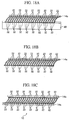
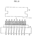
- FIG. 19 is a diagrammatic view illustrating a method for tilting the carbon nanotube bundles.
- the carbon nanotube sheet 10 includes a plurality of carbon nanotube bundles 22, and a coating film 14 formed on both ends thereof.
- the coating film 14 formed on the ends of the neighboring carbon nanotube bundles 22 join each other. That is, the coating film 14 is formed continuous all over both surfaces of the carbon nanotube sheet 10.
- the carbon nanotube bundles 22 are oriented from the side of one surfaces (lower surfaces in the drawing) toward the side of the other surfaces (the upper surfaces in the drawing) and tilted in the same direction intersecting the direction perpendicular to the sheet surface.
- the carbon nanotube bundles 22 neighboring each other in the tilting direction are in contact with each other near at least one ends (upper side in the drawing).
- Each carbon nanotube bundle 22 includes a plurality of carbon nanotubes (not illustrated) oriented in the direction of orientation of the carbon nanotube bundle 22.
- the carbon nanotubes contained in each carbon nanotube bundle 22 can be either of single-walled carbon nanotubes and multi-walled carbon nanotubes.
- the density of the carbon nanotubes contained in each carbon nanotube bundles 22 is preferably above 1 ⁇ 10 10 tubes/cm 2 in terms of the heat radiation and electric conductivity.
- the length of the carbon nanotubes is determined depending on applications of the carbon nanotube sheet 10 and is not especially limited.
- the length of the carbon nanotubes can be set preferably at about 5 - 500 ⁇ m.
- the material of the coating films 14 formed on both surfaces of the carbon nanotube sheet 10 is not especially limited as long as the material has a high thermal conductivity of, e.g., not less than 1 (W/m ⁇ K).
- the material having a thermal conductivity of not less than 1 (W/m ⁇ K) is based on that the thermal conductivity has a sufficiently higher than the thermal conductivity of the general resin materials (about 0.1 (W/m ⁇ K)).
- materials having electric conductivity e.g., metals, alloys, etc. can be used.
- the coating film 14 may not essentially have a single layer structure and may have a layer structure of two layers, or three or more layers, e.g., the layer structure of titanium (Ti) and gold (Au).
- the carbon nanotube bundles 22 are oriented, directed from the side of one surface of the sheet toward the side on the other surface of the sheet. Accordingly, the carbon nanotube sheet which sufficiently exhibits the property of the carbon nanotubes that the thermal conductivity and the electric conductivity in the direction of the orientation are high and has good thermal conductivity and electric conductivity in the direction of the film thickness of the sheet can be realized.
- the carbon nanotubes have also electric conductivity and can be used also as interconnections passed through the sheet. That is, the carbon nanotube sheet according to the present embodiment can be used not only as a heat conductive sheet, but also as a vertical interconnecting sheet.
- the oriented carbon nanotube bundles 22 are tilted in a direction intersecting the direction perpendicular to the sheet surface, and carbon nanotube bundles 22 neighboring in the direction of the tilt are in contact with each other near at least one end.
- the thermal conductivity and the electric conductivity in the direction perpendicular to the sheet surface can be further improved, and the thermal conductivity and the electric conductivity in the direction parallel with the sheet surface can be also improved.
- the neighboring carbon nanotube bundles 22 are contacted with each other, whereby those of the carbon nanotube bundles 22 which are not in direct contact with a mounted body are caused to function as heat conductors and electric conductors indirectly via the other carbon nanotube bundles 22.
- the manufacturing method which will be described later is used, whereby the uniformity of the height of the tilted carbon nanotube bundles 22 can be improved, and the contact area with a mounted body can be increased. Tilting the carbon nanotube bundles 22 has the effect of improving the density of the carbon nanotube bundles 22. Owing to such various effects, the thermal conductivity and the electric conductivity in the direction perpendicular to the sheet surface can be further improved.
- the neighboring carbon nanotube bundles 22 are in contact with each other, whereby a path of the thermal conduction and the electric conduction via the carbon nanotube bundles 22 is formed also in the direction parallel with the sheet surface, and the thermal conductivity and the electric conductivity in the direction parallel with the sheet surface can be also improved.
- the coating film 14 of high thermal conductivity is provided on both surfaces of the carbon nanotube sheet 10, whereby the contact area of the carbon nanotube sheet 10 with respect to a mounted body (heat generator or a heat radiator) can be increased in comparison with the contact area without the coating films 14.
- a mounted body heat generator or a heat radiator
- the coating film 14 has the effect of increasing the contact area between the carbon nanotube bundles 22 and a mounted body and the effect of ensuring the connection between the neighboring carbon nanotube bundles 22.
- the coating film 14 is provided, whereby the thermal contact resistance and contact resistance between the carbon nanotube sheet with a mounted body can be decreased.
- the coating film 14 By using, as the coating film 14, a low melting point material, e.g., indium, low melting point solder or others, the coating film 14 can be reflowed after the carbon nanotube sheet 10 is contacted to the mounted body.
- a low melting point material e.g., indium, low melting point solder or others
- the coating film 14 can be reflowed after the carbon nanotube sheet 10 is contacted to the mounted body.
- concavities and convexities of the joint between the carbon nanotube sheet 10 and a mounted body can be filled by the coating films 14, and the thermal conductivity and the electric conductivity between them can be further improved.
- the filling layer 16 is not formed, as is not in the fifth embodiment. This is because the coating film 14 is formed all over the surfaces, whereby the carbon nanotube bundles 22 (carbon nanotubes) can be supported by the coating film 14.
- the major role of the filling layer 16 is to support the carbon nanotube bundles, retaining the orientation. Accordingly, the filling layer 16 is not essential in the present embodiment, in which the carbon nanotube bundles 22 (carbon nanotubes) can be supported by the coating films 14. However, in the carbon nanotube sheet according to the present embodiment as well, the filling layer 16 may be formed.
- the film thickness of the coating film 14 can be set suitably depending on characteristics, etc. required of the carbon nanotube sheet 10. In terms of supporting the carbon nanotube bundles 22, the film thickness is set preferably at not less than some ⁇ m.
- the substrate 30 to be used as the base for forming the carbon nanotube sheet 10 is prepared.
- the catalyst metal film 32 is selectively formed by, e.g., lift-off method using a photoresist film.
- the regions where the catalyst metal film 32 is formed are the regions for the carbon nanotube bundles 22 to be formed on ( FIG. 17A ).
- the method for forming the catalyst metal film 32 is not essentially limited to lift-off method.
- a metal mask having openings in the regions for the carbon nanotube bundles 22 to be formed on may be used.
- a catalyst metal is sputtered to form the catalyst metal film 32 selectively in the regions for the carbon nanotube bundles 22 to be formed in.
- the plane layout of the catalyst metal film 32 is not especially limited.
- the layout of closed-packed arrangement of circular regions for the carbon nanotube bundles 22 to be formed in can be used.
- the carbon nanotubes are grown by, e.g., hot filament CVD method with the catalyst metal film 32 used as the catalyst.
- the carbon nanotube bundles 22 containing a plurality of carbon nanotubes oriented in the direction of the normal of the substrate 30 (perpendicular orientation) are selectively formed ( FIG. 17B ).
- the thus-grown carbon nanotube bundles 22 are tilted in a direction intersecting the direction perpendicular to the sheet surface ( FIG. 17C ).
- an apparatus which can apply a uniform pressure to the surface of the substrate 30 and can shift the substrate 30 in the horizontal direction under the pressure is used.
- Such apparatus is not especially limited, but the flip chip bonder, for example, can be used.
- the method for tilting the carbon nanotube bundles 22 will be explained here by means of an example using the flip chip bonder.
- the substrate 30 with the carbon nanotube bundles 22 grown on is placed on the stage 50 of the flip chip bonder (see FIG. 19 ).
- the first pressure of about ⁇ some N/cm 2 is applied from above the carbon nanotube bundles 22 perpendicularly to the surface of the substrate 30 (downward in the drawing) (see FIG. 19 ).
- the pressure head 52 has a surface parallel with the substrate 30 as exemplified in FIG. 19 .
- the pressure head 52 is shifted in the first direction parallel with the surface of the substrate 30 (to the right in the drawing) by about tens microns, e.g., 30 ⁇ m (see FIG. 19 ).
- the pressure to be applied by the pressure head 52 is increased from the first pressure to the second pressure which is higher by about 10 - 50 N/cm 2 than the first pressured.
- the first pressure may be increased to the second pressure interruptedly or may be increased gradually in steps to the second pressure.
- the pressure head 52 is shifted by some millimeters, e.g., 2 mm in the first direction parallel with the surface of the substrate 30.
- the pressure to be applied to the carbon nanotube bundles 22 and the shift of the pressure head are made on two stages. This is for tilting the carbon nanotube bundles 22 to a required configuration while preventing the carbon nanotube bundles 22 from being broken.
- the pressure head 52 When the pressure is applied perpendicularly with the carbon nanotube bundles 22 oriented perpendicularly, if the applied pressure is too strong, the carbon nanotube bundles 22 are often collapsed or fractured. Then, in the first stage, the pressure head 52 is pressed against the upper ends of the carbon nanotube bundles 22 with a pressure which does not break the carbon nanotube bundles 22 to be close contact with the carbon nanotube bundles 22. Then, in this state, the pressure head 52 is shifted horizontally to thereby a little tilt the carbon nanotube bundles 22. Because of the pressure head 52 contacting the upper ends of the carbon nanotube bundles 22, tilting the carbon nanotube bundles 22 has the effect of make uniform the carbon nanotube bundles 22 of various heights.
- the pressure applied to the carbon nanotube bundles 22 is distributed, which makes it possible to apply high pressure without breaking the carbon nanotube bundles 22.
- the pressure head 52 is pressed against the upper ends of the carbon nanotube bundles 22, and in this state, the pressure head 52 is horizontally shifted to thereby tilt the carbon nanotube bundles 22 to a prescribed configuration.
- the pressure to be applied to the carbon nanotube bundles 22, and the shift direction and the shift distance of the pressure head 52 can be controlled while monitoring with the flip chip bonder.
- the inventors of the present application made a test on a sample comprising the carbon nanotube bundles 22 of carbon nanotubes formed in a 100 ⁇ m length and a 1 ⁇ 10 11 /cm 2 area density, which are formed on the substrate 30 of a 2 ⁇ 3 cm 2 size by 63% of the area.
- the first pressure the pressure of some N/cm 2 , e.g., 3 N/cm 2 was suitable.
- the second pressure the pressure of tens N/cm 2 , e.g., 40 N/cm 2 was suitable.
- the first and the second pressures to be applied to the carbon nanotube bundles 22 are set suitable so as not to break the carbon nanotube bundles 22, depending on the length of the carbon nanotube bundles 22, the area density of the carbon nanotubes in the carbon nanotube bundles 22, the area density of the carbon nanotube bundles 22, etc.
- the horizontal shift distance of the pressure head 52 is also set suitably depending on the horizontal shift distance of the pressure head 52, the length of the carbon nanotube bundles 22, the required tilt angle of the carbon nanotube bundles, etc.
- the pressure head 52 is shifted, but the pressure head 52 may be shifted to be positioned relative to the substrate 30. That is, the pressure head 52 may be shifted with the stage 50 fixed, the stage 50 may be shifted with the pressure head 52 fixed, or the stage 50 and the pressure head 52 may be shifted in directions opposite to each other.
- the In film is deposited over the carbon nanotube bundles 22 while the In film formed over the neighboring carbon nanotube bundles 22 joins each other, and the coating film 14a of In is formed all over the surface ( FIG. 18A ).
- the constituent material of the coating film 14a is not especially limited as long as the material has high thermal conductivity.
- materials of electric conductivity e.g., metals, alloys, etc. can be used.
- the constituent material of the coating film 14a for example, copper (Cu), nickel (Ni), gold (Au), indium (In), low melting point solder, etc. can be used.
- the coating film 14a may have the single structure of these metals or the layer structure of two layers, or three or more layers, such as the above-described layer structure of titanium and gold.
- the carbon nanotube bundles 22 and the coating film 14a are peeled from the substrate 30 ( FIG. 18B ).
- the In film is deposited over the carbon nanotube bundles 22, and the In film formed over the neighboring carbon nanotube bundles 22 joins each other, and the coating film 14b of In is formed continuous all over the surface.
- the constituent material of the coating film 14b is not especially limited as long as the material has high thermal conductivity.
- materials having electric conductivity e.g., metals, alloys, etc. can be used.
- the constituent material of the coating film 14b for example, copper (Cu), nickel (Ni), gold (Au), indium (In), low melting pint solder, etc. can be used.
- the coating film 14b may have the single layer structure of these metals or the layer structure of two layers, or three or more layers, such as the above-described layer structure of titanium and gold, etc.
- the catalyst metal layer 32 used in the growth is illustrated on the lower ends of the carbon nanotube bundles 22.
- the catalyst metal film 32 coheres in the growth of the carbon nanotubes to be taken into the carbon nanotubes. Actually, the catalyst metal film 32 does not remain in the illustrated state, and the carbon nanotube bundles 22 are exposed on the lower surface of the sheet. The catalyst metal film 32 is often removed simultaneously with peeling the substrate 30.
- the coating films of the material of high thermal conductivity is formed on the ends of the carbon nanotube bundles, whereby the thermal contact resistance and the contact resistance between the carbon nanotube bundles and a sheet mounted body can be drastically decreased.
- the heat conduction and the electric conduction of the carbon nanotube sheet can be improved.
- the carbon nanotube bundles are oriented from one surface of the sheet toward the other surface thereof, and the neighboring carbon nanotube bundles is joined, whereby the sheet of high heat conduction and high electric conduction in the direction perpendicular to the sheet surface and in the direction parallel to the sheet surface can be manufactured.
- the electronic device according to a seventh embodiment will be explained with reference to FIG. 20 .
- FIG. 20 is a diagrammatic sectional view of the electronic device according to the present embodiment, which illustrates the structure thereof.
- the electronic device the carbon nanotube sheet according to any one of the first to the sixth embodiments is applied to as the heat conduction sheet will be explained.
- circuit board 100 such as a multi-level interconnection circuit board or others.
- semiconductor element 106 e.g., a CPU, etc. is mounted on a circuit board 100.
- the semiconductor element 106 is electrically connected to the circuit board 100 via solder bumps 102, and an under fill 104 is filled between the circuit board 100 and the semiconductor element 106.
- a heat spreader 110 for diffusing the heat from the semiconductor element 106 is formed, covering the semiconductor element 106.
- the carbon nanotube sheet 108 according to any one of the first to the sixth embodiments is formed.
- a heat sink 114 for radiating the heat conducted to the heat spreader 110 is formed on the heat spreader 110.
- the carbon nanotube sheet 112 according to any one of the first to the sixth embodiments is formed.
- the carbon nanotube sheets 108, 112 are provided respectively between the semiconductor element 106 and the heat spreader 110 and between the heat spreader 110 and the heat sink 114, i.e., between the heat generation unit and the heat radiation unit.
- the carbon nanotubes are oriented perpendicularly to the film surface of the sheet, and have very high perpendicular heat conduction.
- the carbon nanotube sheet according to the fifth and the sixth embodiments has the coating films 14 formed on both surfaces, and can drastically decrease the thermal contact resistance.
- the described carbon nanotube sheet is used as the heat conduction sheet between the semiconductor element 106 and the heat spreader 110 and between the heat spreader 110 and the heat sink 114, whereby the heat generated from the semiconductor element 106 can be efficiently spread horizontally while being conducted perpendicularly to the heat spreader 110 and the heat sink 114, whereby the heat radiation efficiently can be improved.
- the reliability of the electronic device can be improved.
- the carbon nanotube sheet according to the first to the sixth embodiments is arranged between the semiconductor element and the heat spreader and between the heat spreader and the heat sink, whereby the heat conduction between them can be drastically improved.
- the heat radiation efficiency of the heat generated from the semiconductor element can be increased, and the reliability of the electronic device can be improved.
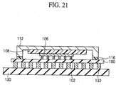
- the electronic device according to an eighth embodiment will be explained with reference to FIG. 21 .
- FIG. 21 is a diagrammatic sectional view illustrating a structure of the electronic device according to the present embodiment.
- the electronic device the carbon nanotube sheet according to any one of the first to the sixth embodiments is applied to as the heat conduction sheet will be explained.
- a circuit board 100 such as a multi-level interconnection circuit board or others, is mounted.
- the circuit board 100 is electrically connected to the printed circuit board 130 via solder bumps 132.
- semiconductor element 106 e.g., a CPU, etc. are mounted on the circuit board 100.
- the semiconductor element 106 is electrically connected to the circuit board 100 via solder bumps 102.
- a heat spreader 110 for diffusing the heat from the semiconductor element 106 is formed, covering the semiconductor element 106.
- the carbon nanotube sheet 108 according to any one of the first to the sixth embodiments is formed between the semiconductor element 106 and the heat spreader 110.
- the heat spreader 110 is adhered to the circuit board 100 with, e.g., an organic sealant 116.
- the carbon nanotube sheet 108 according to any one of the first to the sixth embodiments is provided between the semiconductor element 106 and the heat spreader 110, i.e., the heat generation unit and the heat radiation unit.
- carbon nanotube sheet according to the first to the sixth embodiments the carbon nanotubes are oriented perpendicularly to the film surface of the sheet, and the coating films 14 for decreasing the thermal contact resistance is formed on both ends.
- the heat conduction perpendicular to the surface is very high.
- the described carbon nanotube sheet is used as the heat conduction sheet formed between the semiconductor element 106 and the heat spreader 110, whereby the heat generated from the semiconductor element 106 can be efficiently spread horizontally while being conducted perpendicularly to the heat spreader 110 and the heat sink 114, and the heat radiation efficiently can be improved.
- the reliability of the electronic device can be improved.
- the coating films 14 formed on both surfaces of the sheet materials, such as indium and low melting point, solder whose melting points are lower than those of the materials of the other constituent parts of the electronic device, e.g., the solder bumps 102, 132 and the organic sealant 116 are used, whereby the heat radiation efficiency can be further increased.
- the coating films 14 are formed of a material having a low melting point, e.g., a low melting point material, e.g., indium, low melting point solder or others than the materials of the other constituent parts of the electronic device, whereby the coating film can be reflowed without damaging the other constituent parts.
- a low melting point material e.g., indium, low melting point solder or others
- convexities and concavities of the interface between the semiconductor element 106 and the carbon nanotube sheet 108 and those of the interface between the carbon nanotube sheet 108 and the heat spreader 110 can be filled with the constituent material of the coating films 14, and the thermal contact resistance between them can be further decreased.
- the thermal processing step for reflowing the coating films 14 can be made, e.g., after the heat spreader 110 has been adhered onto the circuit board 100 or after the circuit board 100 has been mounted on the printed board 130.
- the carbon nanotube sheet according to any one of the first to the sixth embodiments is provided between the semiconductor element and the heat spreader, whereby the heat conduction between them can be drastically improved.
- the heat radiation efficiency of the heat generated from the semiconductor element can be increased, the reliability of the electronic device can be improved.
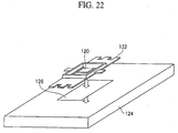
- the electronic device according to a ninth embodiment will be explained with reference to FIG. 22 .
- FIG. 22 is a perspective view illustrating a structure of the electronic device according to the present embodiment.
- the electronic device using the carbon nanotube sheet according to any one of the first to the sixth embodiments as the heat conductive sheet which functions also the electric conductive sheet will be explained.
- the HPA (High Power Amplifier) 120 used in radio communication stations, etc. is incorporated in a package 122, and a heat sink 124 is jointed to the underside of the package 122.
- the heat generated from the HPA 120 is radiated to the heat sink 124 through the underside of the package 122.
- the package 122 is also used as the electric ground and must be electrically connected to the heat sink 124.
- a good conductor for electricity and heat is used to joint the package 122 and the heat sink 124.
- the carbon nanotube sheet 126 As illustrated in FIG. 22 , at the joint between the package 122 and the heat sink 124, the carbon nanotube sheet 126 according to any one of the first to the sixth embodiments is used to thereby electrically connect the package 122 and the heat sink 124.
- the heat generated from the HPA 120 can be efficiently conducted to the heat sink 124, and the heat radiation efficiency can be improved. Thus, the reliability of the electronic device can be improved.
- the carbon nanotube sheet having carbon nanotubes oriented in the direction of the film thickness of the sheet is provided between the package of the HPA and the heat sink, whereby the thermal conductivity between them can be drastically improved.
- the heat radiation of the heat generated from the HPA can be improved, and the reliability of the electronic device can be increased.
- the HPA, and the heat sink as the ground can be electrically connected.
- the sheet structure using the linear structure of carbon atoms is exemplified by carbon nanotube sheet using carbon nanotubes, but the sheet structure using the linear structure of carbon atoms is not limited to this.
- the linear structure of carbon atoms other than carbon nanotubes, carbon nanowires, carbon rods and carbon fibers are listed. These linear structures are the same as the carbon nanotubes except that they are different from the carbon nanotubes in size. The embodiments are applicable to the sheet structures using these linear structures.
- the coating films 14 are provided on both surfaces of the carbon nanotube sheet 10, but the coating film 14 may be formed only one surface of the carbon nanotube sheet 10.
- the coating film 14 formed only one surface of the carbon nanotube sheet 10 when the carbon nanotube sheet 10 is used as heat conduction sheet, it is preferable to arrange the carbon nanotube sheet 20 with the surface with the coating film 14 formed on positioned on the side of a heat generator.
- the carbon nanotube sheet 10 having the coating film 14 formed only one surface can be formed by filling the filling layer 16 and peeling the sheet from the substrate after the step of FIG. 5A .
- the filling layer 16 is formed between the carbon nanotubes 12 or between the carbon nanotube bundles 22, but the filling layer 16 may not be essentially formed.
- the filling layer 16 is mainly for supporting a plurality of carbon nanotubes 12 or a plurality of carbon nanotube bundles 22 to maintain the state of the sheet. Accordingly, for example, when the coating film 14 is formed continuous on the surface of the sheet and can sufficiently support the carbon nanotubes 12, the filing layer 16 may not be essentially formed.
- the carbon nanotube bundles 22 are tilted. Also in the carbon nanotube sheet 10 having the carbon nanotubes 12 formed all over the surface as in, e.g., the first to the third embodiments and the fifth embodiment, the carbon nanotubes 12 may be tilted. The carbon nanotubes 12 can be tilted by, e.g., the method described in the sixth embodiment.
- the uses of the carbon nanotube sheet are not limited to those described in the embodiments described above.
- the described carbon nanotube sheet is applicable, as the heat conduction sheet, to, e.g., the heat radiation sheet of CPUs, high power amplifiers of radio communication stations, high power amplifiers for radio communication terminals, high power switches for electric motors, servers, personal computers, etc.
- the carbon nanotube sheet can be applicable to vertical interconnecting sheets and various applications using the vertical interconnection sheets.
Landscapes
- Chemical & Material Sciences (AREA)
- Engineering & Computer Science (AREA)
- Crystallography & Structural Chemistry (AREA)
- Nanotechnology (AREA)
- Combustion & Propulsion (AREA)
- Thermal Sciences (AREA)
- Materials Engineering (AREA)
- Organic Chemistry (AREA)
- Physics & Mathematics (AREA)
- Chemical Kinetics & Catalysis (AREA)
- Manufacturing & Machinery (AREA)
- Cooling Or The Like Of Semiconductors Or Solid State Devices (AREA)
- Carbon And Carbon Compounds (AREA)
- Secondary Cells (AREA)
- Laminated Bodies (AREA)
- Fuel Cell (AREA)
- Cooling Or The Like Of Electrical Apparatus (AREA)
Claims (14)
- Structure de feuille (10) comprenant :plusieurs structures linéaires (12) d'atomes de carbone ; etun premier film de revêtement (14 ; 14a) formé sur au moins une extrémité des plusieurs structures linéaires (12), et formé d'un matériau présentant une conductivité thermique supérieure d'au moins 1 W/m·K et joignant les structures linéaires (12) voisines les unes des autres,caractérisée par une longueur (Lc) d'une région des plusieurs structures linéaires (12) recouverte par le premier film de revêtement (14 ; 14a) n'étant pas inférieure à 100 nm.
- Structure de feuille (10) selon la revendication 1, comprenant de plus :une couche de remplissage (16) introduite dans des espaces entre les plusieurs structures linéaires (12) et supportant les plusieurs structures linéaires (12) ;dans laquelle le premier film de revêtement (14 ; 14a) est formé d'un matériau présentant une conductivité thermique supérieure à un matériau de constituant de la couche de remplissage (16).
- Structure de feuille selon l'une quelconque des revendications 1 ou 2, comprenant de plus
une couche de graphite (20) formée entre le premier film de revêtement (14 ; 14a) et les structures linéaires (12). - Structure de feuille selon l'une quelconque des revendications 1 à 3, comprenant de plus
un second film de revêtement (14b) formé sur l'autre extrémité des plusieurs structures linéaires (12). - Structure de feuille selon l'une quelconque des revendications 1 à 4, dans laquelle
les plusieurs structures linéaires (12) sont disposées avec un premier espace les unes avec les autres et forment plusieurs faisceaux de structures linéaires (22) disposés avec un second espace les uns avec les autres, lequel est plus grand que le premier espace. - Structure de feuille selon l'une quelconque des revendications 1 à 5, dans laquelle
les plusieurs structures linéaires (12) sont orientées dans une direction d'une épaisseur de film de la feuille (10). - Structure de feuille selon l'une quelconque des revendications 1 à 6, dans laquelle
les plusieurs structures linéaires (12) sont inclinées par rapport à la direction d'une épaisseur de film de la feuille (10) et dans la même direction, et les structures linéaires voisines (12) sont en contact les unes avec les autres. - Structure de feuille selon la revendication 4, ou l'une quelconque des revendications 5 à 7 lorsqu'elle est lue comme annexée dans la revendication 4, dans laquelle
le second film de revêtement (14b) présente une conductivité thermique qui n'est pas inférieure à 1 W/m.K. - Dispositif électronique comprenant :un générateur de chaleur ;un radiateur de chaleur pour irradier de la chaleur provenant du générateur de chaleur ; etune structure de feuille (10) disposée entre le générateur de chaleur et le radiateur de chaleur, et comprenant :plusieurs structures linéaires (12) d'atomes de carbone ;un premier film de revêtement (14 ; 14a) formé sur une extrémité des plusieurs structures linéaires (12), et formé d'un matériau présentant une conductivité thermique supérieure qui n'est pas inférieure à 1 W/m.K, une longueur (Lc) d'une région des plusieurs structures linéaires (12) recouverte par le premier film de revêtement (14a) qui n'est pas inférieure à 100 nm ; etun second film de revêtement (14b) formé sur l'autre extrémité des plusieurs structures linéaires (12), et formé d'un matériau présentant une conductivité thermique supérieure qui n'est pas inférieure à 1 W/m.K, une longueur (Lc) d'une région des plusieurs structures linéaires (12) recouverte par le second film de revêtement (14b) qui n'est pas inférieure à 100 nm.
- Dispositif électronique selon la revendication 9, dans lequel la structure de feuille (10) comprend de plus une couche de remplissage (16) qui est introduite dans des espaces entre les plusieurs structures linéaires (12) et qui supporte les plusieurs structures linéaires (12).
- Dispositif électronique selon la revendication 9, dans lequel le premier film de revêtement (14 ; 14a) et le second film de revêtement (14b) sont formés, joignant les structures linéaires voisines (12) les unes avec les autres, et
les plusieurs structures linéaires (12) sont supportées par les premier et second films de revêtement. - Procédé de fabrication d'une structure de feuille (10) comprenant :la formation d'un film de métal de catalyseur (32) sur un premier substrat (30) ;la croissance sur le premier substrat (30) de plusieurs structures linéaires (12) d'atomes de carbone avec le film de métal de catalyseur (32) comme un catalyseur ;la formation d'un premier film de revêtement (14 ; 14a) sur une extrémité des plusieurs structures linéaires (12) pour joindre les structures linéaires voisines (12) de sorte qu'une longueur (Lc) d'une région des plusieurs structures linéaires (12) recouverte par le premier film de revêtement (14 ; 14a) n'est pas inférieure à 100 nm ; etle prélèvement du premier substrat (30) de l'interface entre les plusieurs structures linéaires (12) et le premier substrat (30).
- Procédé de fabrication d'une structure de feuille (10) selon la revendication 12, comprenant de plus :avant le prélèvement du premier substrat (30), l'adhérence d'un second substrat (40) au premier film de revêtement (14a) ;après le prélèvement du premier substrat (30), le remplissage d'un matériau de remplissage entre les structures linéaires (12) pour former une couche de remplissage (16) ; etle prélèvement du second substrat (40).
- Procédé de fabrication d'un dispositif électronique comprenant :la jonction d'un générateur de chaleur, et d'un radiateur de chaleur pour irradier de la chaleur générée par le générateur de chaleur avec une structure de feuille (10) disposée entre ceux-ci, la structure de feuille (10) comprenant plusieurs structures linéaires (12) d'atomes de carbone, un premier film de revêtement (14a) formé sur une extrémité des plusieurs structures linéaires (12) et un second film de revêtement (14b) formé sur l'autre extrémité des plusieurs structures linéaires (12) ; etla réalisation d'un traitement thermique à une température supérieure à un point de fusion d'un matériau de constituant des premier film de revêtement (14a) et second film de revêtement (14b) pour refusionner le premier film de revêtement (14) et le second film de revêtement (14b).
Applications Claiming Priority (2)
| Application Number | Priority Date | Filing Date | Title |
|---|---|---|---|
| JP2008068992 | 2008-03-18 | ||
| JP2008275338A JP5146256B2 (ja) | 2008-03-18 | 2008-10-27 | シート状構造体及びその製造方法、並びに電子機器及びその製造方法 |
Publications (3)
| Publication Number | Publication Date |
|---|---|
| EP2104141A2 EP2104141A2 (fr) | 2009-09-23 |
| EP2104141A3 EP2104141A3 (fr) | 2010-10-27 |
| EP2104141B1 true EP2104141B1 (fr) | 2016-05-18 |
Family
ID=40651768
Family Applications (1)
| Application Number | Title | Priority Date | Filing Date |
|---|---|---|---|
| EP09155530.0A Active EP2104141B1 (fr) | 2008-03-18 | 2009-03-18 | Structure de feuille et procédé de fabrication associée |
Country Status (6)
| Country | Link |
|---|---|
| US (1) | US8749979B2 (fr) |
| EP (1) | EP2104141B1 (fr) |
| JP (1) | JP5146256B2 (fr) |
| KR (1) | KR101051351B1 (fr) |
| CN (1) | CN101540302B (fr) |
| TW (1) | TWI398508B (fr) |
Families Citing this family (72)
| Publication number | Priority date | Publication date | Assignee | Title |
|---|---|---|---|---|
| EP2570385A3 (fr) * | 2005-05-03 | 2013-10-16 | Nanocomp Technologies, Inc. | Matériaux en composites de carbone et leurs procédés de fabrication |
| CA2850951A1 (fr) | 2005-07-28 | 2007-01-28 | Nanocomp Technologies, Inc. | Systemes et methodes pour la formation et la collecte de materiaux nanofibreux |
| EP2125359B1 (fr) * | 2007-02-27 | 2016-07-27 | Nanocomp Technologies, Inc. | Matériaux pour protection thermique et procédés de fabrication de ceux-ci |
| US9061913B2 (en) | 2007-06-15 | 2015-06-23 | Nanocomp Technologies, Inc. | Injector apparatus and methods for production of nanostructures |
| EP2173655B1 (fr) * | 2007-07-09 | 2020-04-08 | Nanocomp Technologies, Inc. | Alignement chimiquement assisté de nanotubes dans des structures extensibles |
| WO2009021069A1 (fr) * | 2007-08-07 | 2009-02-12 | Nanocomp Technologies, Inc. | Adaptateurs à base de nanostructures électriquement et thermiquement conductrices non métalliques |
| JP2010537410A (ja) * | 2007-08-14 | 2010-12-02 | ナノコンプ テクノロジーズ インコーポレイテッド | ナノ構造材料ベースの熱電発電装置 |
| JP5864253B2 (ja) * | 2008-05-07 | 2016-02-17 | ナノコンプ テクノロジーズ インコーポレイテッド | ナノ構造複合材シートの形成方法 |
| AU2009244152A1 (en) | 2008-05-07 | 2009-11-12 | Nanocomp Technologies, Inc. | Nanostructure-based heating devices and method of use |
| US8304291B2 (en) * | 2009-06-29 | 2012-11-06 | Advanced Micro Devices, Inc. | Semiconductor chip thermal interface structures |
| US8405996B2 (en) * | 2009-06-30 | 2013-03-26 | General Electric Company | Article including thermal interface element and method of preparation |
| US8354593B2 (en) * | 2009-07-10 | 2013-01-15 | Nanocomp Technologies, Inc. | Hybrid conductors and method of making same |
| US8106510B2 (en) | 2009-08-04 | 2012-01-31 | Raytheon Company | Nano-tube thermal interface structure |
| KR101007057B1 (ko) * | 2009-10-08 | 2011-01-12 | 동국대학교 산학협력단 | 나노구조를 갖는 mim 캐패시터 제조방법 |
| JP5356972B2 (ja) * | 2009-10-20 | 2013-12-04 | 新光電気工業株式会社 | 放熱用部品及びその製造方法、半導体パッケージ |
| CN101747869A (zh) * | 2009-12-18 | 2010-06-23 | 东南大学 | 热界面材料 |
| CN102107546B (zh) * | 2009-12-29 | 2013-04-24 | 北京富纳特创新科技有限公司 | 汽车玻璃贴膜及汽车 |
| JP5673668B2 (ja) * | 2010-03-12 | 2015-02-18 | 富士通株式会社 | 放熱構造体、電子機器およびそれらの製造方法 |
| JP5447069B2 (ja) * | 2010-03-24 | 2014-03-19 | 富士通株式会社 | シート状構造体、電子機器及び電子機器の製造方法 |
| JP5447117B2 (ja) * | 2010-04-09 | 2014-03-19 | 富士通株式会社 | 電子機器の製造方法 |
| KR101050198B1 (ko) | 2010-07-26 | 2011-07-19 | 연세대학교 산학협력단 | 나노선 다이오드 생성 방법 |
| US8722171B2 (en) | 2011-01-04 | 2014-05-13 | Nanocomp Technologies, Inc. | Nanotube-based insulators |
| JP5714928B2 (ja) * | 2011-02-09 | 2015-05-07 | 日東電工株式会社 | 繊維状柱状構造体集合体および放熱部材 |
| JP6132768B2 (ja) * | 2011-09-26 | 2017-05-24 | 富士通株式会社 | 放熱材料及びその製造方法 |
| JP5788760B2 (ja) * | 2011-10-19 | 2015-10-07 | 日東電工株式会社 | 熱伝導性シート、led実装用基板およびledモジュール |
| JP5935302B2 (ja) * | 2011-11-18 | 2016-06-15 | 富士通株式会社 | シート状構造体及びその製造方法並びに電子機器及びその製造方法 |
| CN103178027B (zh) * | 2011-12-21 | 2016-03-09 | 清华大学 | 散热结构及应用该散热结构的电子设备 |
| FR2985603B1 (fr) * | 2012-01-10 | 2016-12-23 | Commissariat Energie Atomique | Dispositif de gestion thermique passif |
| JP5998557B2 (ja) * | 2012-03-23 | 2016-09-28 | 富士通株式会社 | 放熱シートの製造方法 |
| FR2995877B1 (fr) * | 2012-09-21 | 2014-10-24 | Thales Sa | Structure meca-thermique adaptee pour un environnement spatial |
| JP6118540B2 (ja) * | 2012-11-08 | 2017-04-19 | 新光電気工業株式会社 | 放熱部品及びその製造方法 |
| US20140151009A1 (en) * | 2012-11-30 | 2014-06-05 | General Electric Company | Thermal interface element and method of preparation |
| EP2945189A4 (fr) * | 2013-01-09 | 2016-11-16 | Hitachi Ltd | Dispositif à semi-conducteurs et son procédé de fabrication |
| JP6115270B2 (ja) * | 2013-04-09 | 2017-04-19 | 富士通株式会社 | 放熱構造体及びその製造方法並びに電子装置 |
| CN105247674B (zh) * | 2013-06-03 | 2018-04-13 | 富士通株式会社 | 散热结构体及其制造方法以及电子装置 |
| WO2014204561A1 (fr) | 2013-06-17 | 2014-12-24 | Nanocomp Technologies, Inc. | Agents exfoliants-dispersants pour nanotubes, faisceaux et fibres |
| JP6186933B2 (ja) * | 2013-06-21 | 2017-08-30 | 富士通株式会社 | 接合シート及びその製造方法、並びに放熱機構及びその製造方法 |
| CN103367275B (zh) * | 2013-07-10 | 2016-10-05 | 华为技术有限公司 | 一种界面导热片及其制备方法、散热系统 |
| WO2015045648A1 (fr) * | 2013-09-30 | 2015-04-02 | 富士電機株式会社 | Dispositif à semi-conducteurs, procédé d'assemblage d'un dispositif à semi-conducteurs, composant pour des dispositifs à semi-conducteurs, et module unitaire |
| US9905658B2 (en) * | 2013-11-26 | 2018-02-27 | Nxp Usa, Inc. | Transistors with field plates resistant to field plate material migration and methods of their fabrication |
| US10839975B2 (en) | 2014-03-10 | 2020-11-17 | The Boeing Company | Graphene coated electronic components |
| US9930808B2 (en) * | 2014-03-10 | 2018-03-27 | The Boeing Company | Graphene-based thermal management systems |
| JP6223903B2 (ja) * | 2014-04-30 | 2017-11-01 | 新光電気工業株式会社 | カーボンナノチューブシート及び電子機器とカーボンナノチューブシートの製造方法及び電子機器の製造方法 |
| US9482477B2 (en) * | 2014-07-28 | 2016-11-01 | Northrop Grumman Systems Corporation | Nano-thermal agents for enhanced interfacial thermal conductance |
| JP6295238B2 (ja) | 2014-10-31 | 2018-03-14 | デクセリアルズ株式会社 | 熱伝導シート、熱伝導シートの製造方法、放熱部材及び半導体装置 |
| EP3253709A4 (fr) | 2015-02-03 | 2018-10-31 | Nanocomp Technologies, Inc. | Structures à nanotubes de carbone et procédés de production de ceux-ci |
| US9468989B2 (en) * | 2015-02-26 | 2016-10-18 | Northrop Grumman Systems Corporation | High-conductivity bonding of metal nanowire arrays |
| FR3041274B1 (fr) * | 2015-09-17 | 2017-09-29 | Commissariat Energie Atomique | Procede d'orientation d'objets allonges disposes en surface d'un substrat |
| JP6582854B2 (ja) * | 2015-10-14 | 2019-10-02 | 富士通株式会社 | 放熱シート、放熱シートの製造方法、及び電子装置 |
| JP6301978B2 (ja) * | 2016-01-26 | 2018-03-28 | デクセリアルズ株式会社 | 熱伝導シート、熱伝導シートの製造方法、放熱部材及び半導体装置 |
| US10304803B2 (en) * | 2016-05-05 | 2019-05-28 | Invensas Corporation | Nanoscale interconnect array for stacked dies |
| EP3453049A4 (fr) | 2016-05-06 | 2019-12-18 | Smoltek AB | Plate-forme d'assemblage |
| EP3507872A4 (fr) * | 2016-08-30 | 2020-04-15 | Teradiode, Inc. | Conditionnement laser haute puissance utilisant des nanotubes de carbone |
| US10153224B2 (en) * | 2016-09-14 | 2018-12-11 | Globalfoundries Inc. | Backside spacer structures for improved thermal performance |
| DE102016217735A1 (de) * | 2016-09-16 | 2018-03-22 | Carl Zeiss Smt Gmbh | Komponente für eine Spiegelanordnung für die EUV-Lithographie |
| JP6810343B2 (ja) * | 2016-10-17 | 2021-01-06 | 富士通株式会社 | カーボンナノチューブ構造、放熱シート及びカーボンナノチューブ構造の製造方法 |
| US10581082B2 (en) | 2016-11-15 | 2020-03-03 | Nanocomp Technologies, Inc. | Systems and methods for making structures defined by CNT pulp networks |
| CN108251063B (zh) * | 2016-12-28 | 2021-05-11 | 有研工程技术研究院有限公司 | 一种高性能复合相变材料及其制备方法 |
| US11279836B2 (en) | 2017-01-09 | 2022-03-22 | Nanocomp Technologies, Inc. | Intumescent nanostructured materials and methods of manufacturing same |
| JP6901896B2 (ja) * | 2017-03-31 | 2021-07-14 | 日立造船株式会社 | フィラー・樹脂複合体、フィラー・樹脂複合体の製造方法、フィラー・樹脂複合層、および、フィラー・樹脂複合体の使用方法 |
| US20180376618A1 (en) * | 2017-06-27 | 2018-12-27 | Joinset Co., Ltd. | Thermally conductive member |
| CN111115615B (zh) | 2018-11-01 | 2021-08-31 | 清华大学 | 碳纳米管阵列的转移方法 |
| CN111121981B (zh) | 2018-11-01 | 2021-04-02 | 清华大学 | 黑体辐射源的制备方法 |
| CN111128637B (zh) | 2018-11-01 | 2021-02-26 | 清华大学 | 场发射体的制备方法 |
| CN110003438A (zh) * | 2019-03-29 | 2019-07-12 | 傲川科技(河源)有限公司 | 导热凝胶及其制备方法 |
| KR102584991B1 (ko) * | 2019-06-14 | 2023-10-05 | 삼성전기주식회사 | 반도체 패키지 |
| CN110625877B (zh) * | 2019-09-05 | 2021-06-08 | 上海阿莱德实业股份有限公司 | 一种导热界面材料的制备方法 |
| CN114828538A (zh) * | 2021-01-29 | 2022-07-29 | 优材科技有限公司 | 导热黏着结构与电子装置 |
| US12230419B1 (en) | 2021-07-09 | 2025-02-18 | Hrl Laboratories, Llc | Carbon nanotube ultraconductor |
| US20230225084A1 (en) * | 2022-09-30 | 2023-07-13 | Intel Corporation | Methods and apparatus to cool hardware |
| JP2024065820A (ja) * | 2022-10-31 | 2024-05-15 | 株式会社デンソー | 接続構造、半導体装置および絶縁内蔵基板 |
| WO2026048645A1 (fr) * | 2024-08-30 | 2026-03-05 | 東京エレクトロン株式会社 | Feuille de transfert de chaleur, appareil de fabrication de semi-conducteur et procédé de fabrication de feuille de transfert de chaleur |
Family Cites Families (28)
| Publication number | Priority date | Publication date | Assignee | Title |
|---|---|---|---|---|
| JPS5313610A (en) * | 1976-07-23 | 1978-02-07 | Nippon Carbon Co Ltd | Compound sheet materials |
| EP0661916B1 (fr) * | 1993-07-06 | 2000-05-17 | Kabushiki Kaisha Toshiba | Feuille thermoconductrice |
| US6630772B1 (en) | 1998-09-21 | 2003-10-07 | Agere Systems Inc. | Device comprising carbon nanotube field emitter structure and process for forming device |
| GB0008897D0 (en) * | 2000-04-12 | 2000-05-31 | Cheiros Technology Ltd | Improvements relating to heat transfer |
| JP2002141633A (ja) | 2000-10-25 | 2002-05-17 | Lucent Technol Inc | 垂直にナノ相互接続された回路デバイスからなる製品及びその製造方法 |
| US6821625B2 (en) * | 2001-09-27 | 2004-11-23 | International Business Machines Corporation | Thermal spreader using thermal conduits |
| US6965513B2 (en) * | 2001-12-20 | 2005-11-15 | Intel Corporation | Carbon nanotube thermal interface structures |
| US6837273B2 (en) * | 2002-06-19 | 2005-01-04 | Saint-Gobain Technical Fabrics Canada, Ltd. | Inversion liner and liner components for conduits |
| US7095053B2 (en) * | 2003-05-05 | 2006-08-22 | Lamina Ceramics, Inc. | Light emitting diodes packaged for high temperature operation |
| US7112472B2 (en) * | 2003-06-25 | 2006-09-26 | Intel Corporation | Methods of fabricating a composite carbon nanotube thermal interface device |
| US7168484B2 (en) * | 2003-06-30 | 2007-01-30 | Intel Corporation | Thermal interface apparatus, systems, and methods |
| US7077858B2 (en) * | 2003-09-22 | 2006-07-18 | Coolhead Technologies, Inc. | Flexible heat exchangers for medical cooling and warming applications |
| JP4412052B2 (ja) | 2003-10-28 | 2010-02-10 | 富士ゼロックス株式会社 | 複合材およびその製造方法 |
| JP2005150362A (ja) | 2003-11-14 | 2005-06-09 | Dainippon Printing Co Ltd | 高熱伝導性シートおよびその製造方法 |
| US7279916B2 (en) * | 2004-10-05 | 2007-10-09 | Nanoconduction, Inc. | Apparatus and test device for the application and measurement of prescribed, predicted and controlled contact pressure on wires |
| JP2006147801A (ja) | 2004-11-18 | 2006-06-08 | Seiko Precision Inc | 放熱シート、インターフェース、電子部品及び放熱シートの製造方法 |
| CN100337981C (zh) * | 2005-03-24 | 2007-09-19 | 清华大学 | 热界面材料及其制造方法 |
| CN100404242C (zh) * | 2005-04-14 | 2008-07-23 | 清华大学 | 热界面材料及其制造方法 |
| US20060231946A1 (en) * | 2005-04-14 | 2006-10-19 | Molecular Nanosystems, Inc. | Nanotube surface coatings for improved wettability |
| JP2006303240A (ja) | 2005-04-21 | 2006-11-02 | Fujikura Ltd | 放熱シート、放熱体、放熱シート製造方法及び伝熱方法 |
| CN100454526C (zh) * | 2005-06-30 | 2009-01-21 | 鸿富锦精密工业(深圳)有限公司 | 热界面材料制造方法 |
| CN1891780B (zh) * | 2005-07-01 | 2013-04-24 | 清华大学 | 热界面材料及其制备方法 |
| JP4684053B2 (ja) | 2005-09-09 | 2011-05-18 | 株式会社アルバック | カーボンナノチューブの作製方法及びその固定方法 |
| US7505275B2 (en) * | 2005-11-04 | 2009-03-17 | Graftech International Holdings Inc. | LED with integral via |
| WO2007110899A1 (fr) * | 2006-03-24 | 2007-10-04 | Fujitsu Limited | Structure en fibres de carbone et son procédé de fabrication |
| CN101054467B (zh) * | 2006-04-14 | 2010-05-26 | 清华大学 | 碳纳米管复合材料及其制备方法 |
| JP2008034474A (ja) | 2006-07-26 | 2008-02-14 | Sharp Corp | 伝熱シート及び基板装置 |
| US7742673B2 (en) * | 2007-09-28 | 2010-06-22 | General Electric Company | Thermal mangement article having thermal wave guide |
-
2008
- 2008-10-27 JP JP2008275338A patent/JP5146256B2/ja active Active
-
2009
- 2009-03-12 KR KR1020090021322A patent/KR101051351B1/ko active Active
- 2009-03-17 TW TW098108570A patent/TWI398508B/zh active
- 2009-03-17 CN CN2009101280244A patent/CN101540302B/zh active Active
- 2009-03-17 US US12/405,578 patent/US8749979B2/en active Active
- 2009-03-18 EP EP09155530.0A patent/EP2104141B1/fr active Active
Also Published As
| Publication number | Publication date |
|---|---|
| JP2009260238A (ja) | 2009-11-05 |
| US20090237886A1 (en) | 2009-09-24 |
| EP2104141A2 (fr) | 2009-09-23 |
| US8749979B2 (en) | 2014-06-10 |
| KR20090100257A (ko) | 2009-09-23 |
| TWI398508B (zh) | 2013-06-11 |
| CN101540302B (zh) | 2012-04-04 |
| CN101540302A (zh) | 2009-09-23 |
| JP5146256B2 (ja) | 2013-02-20 |
| KR101051351B1 (ko) | 2011-07-22 |
| EP2104141A3 (fr) | 2010-10-27 |
| TW200951210A (en) | 2009-12-16 |
Similar Documents
| Publication | Publication Date | Title |
|---|---|---|
| EP2104141B1 (fr) | Structure de feuille et procédé de fabrication associée | |
| US8958207B2 (en) | Heat radiation material, electronic device and method of manufacturing electronic device | |
| US8743546B2 (en) | Sheet structure and method of manufacturing the same | |
| JP6149077B2 (ja) | ナノ構造体による隣接層の接続および接合 | |
| JP5506657B2 (ja) | シート状構造体、半導体装置及び炭素構造体の成長方法 | |
| WO2011111112A1 (fr) | Structure de dissipation de chaleur, et procédé de fabrication de celle-ci | |
| JP5013116B2 (ja) | シート状構造体及びその製造方法並びに電子機器 | |
| JP5447117B2 (ja) | 電子機器の製造方法 | |
| JP5343620B2 (ja) | 放熱材料及びその製造方法並びに電子機器及びその製造方法 | |
| EP2061077B1 (fr) | Structure de feuille et son procédé de fabrication | |
| JP5768786B2 (ja) | シート状構造体及び電子機器 | |
| US9644128B2 (en) | Carbon nanotube sheet, electronic device, method of manufacturing carbon nanotube sheet, and method of manufacturing electronic device | |
| JP2010280528A (ja) | シート状構造体及びその製造方法 |
Legal Events
| Date | Code | Title | Description |
|---|---|---|---|
| PUAI | Public reference made under article 153(3) epc to a published international application that has entered the european phase |
Free format text: ORIGINAL CODE: 0009012 |
|
| AK | Designated contracting states |
Kind code of ref document: A2 Designated state(s): AT BE BG CH CY CZ DE DK EE ES FI FR GB GR HR HU IE IS IT LI LT LU LV MC MK MT NL NO PL PT RO SE SI SK TR |
|
| AX | Request for extension of the european patent |
Extension state: AL BA RS |
|
| PUAL | Search report despatched |
Free format text: ORIGINAL CODE: 0009013 |
|
| AK | Designated contracting states |
Kind code of ref document: A3 Designated state(s): AT BE BG CH CY CZ DE DK EE ES FI FR GB GR HR HU IE IS IT LI LT LU LV MC MK MT NL NO PL PT RO SE SI SK TR |
|
| AX | Request for extension of the european patent |
Extension state: AL BA RS |
|
| RIC1 | Information provided on ipc code assigned before grant |
Ipc: H01L 23/433 20060101ALI20100917BHEP Ipc: H01L 23/373 20060101AFI20090529BHEP |
|
| 17P | Request for examination filed |
Effective date: 20110420 |
|
| AKX | Designation fees paid |
Designated state(s): DE FR GB IT |
|
| 17Q | First examination report despatched |
Effective date: 20120419 |
|
| GRAP | Despatch of communication of intention to grant a patent |
Free format text: ORIGINAL CODE: EPIDOSNIGR1 |
|
| INTG | Intention to grant announced |
Effective date: 20151208 |
|
| GRAS | Grant fee paid |
Free format text: ORIGINAL CODE: EPIDOSNIGR3 |
|
| GRAA | (expected) grant |
Free format text: ORIGINAL CODE: 0009210 |
|
| AK | Designated contracting states |
Kind code of ref document: B1 Designated state(s): DE FR GB IT |
|
| REG | Reference to a national code |
Ref country code: GB Ref legal event code: FG4D |
|
| REG | Reference to a national code |
Ref country code: DE Ref legal event code: R096 Ref document number: 602009038694 Country of ref document: DE |
|
| REG | Reference to a national code |
Ref country code: FR Ref legal event code: PLFP Year of fee payment: 9 |
|
| REG | Reference to a national code |
Ref country code: DE Ref legal event code: R097 Ref document number: 602009038694 Country of ref document: DE |
|
| PLBE | No opposition filed within time limit |
Free format text: ORIGINAL CODE: 0009261 |
|
| STAA | Information on the status of an ep patent application or granted ep patent |
Free format text: STATUS: NO OPPOSITION FILED WITHIN TIME LIMIT |
|
| 26N | No opposition filed |
Effective date: 20170221 |
|
| REG | Reference to a national code |
Ref country code: FR Ref legal event code: PLFP Year of fee payment: 10 |
|
| REG | Reference to a national code |
Ref country code: DE Ref legal event code: R079 Ref document number: 602009038694 Country of ref document: DE Free format text: PREVIOUS MAIN CLASS: H01L0023373000 Ipc: H10W0040250000 |
|
| PGFP | Annual fee paid to national office [announced via postgrant information from national office to epo] |
Ref country code: GB Payment date: 20260219 Year of fee payment: 18 |
|
| PGFP | Annual fee paid to national office [announced via postgrant information from national office to epo] |
Ref country code: DE Payment date: 20260219 Year of fee payment: 18 |
|
| PGFP | Annual fee paid to national office [announced via postgrant information from national office to epo] |
Ref country code: IT Payment date: 20260219 Year of fee payment: 18 |
|
| PGFP | Annual fee paid to national office [announced via postgrant information from national office to epo] |
Ref country code: FR Payment date: 20260219 Year of fee payment: 18 |