EP2106044A1 - Système de transmission optique avec pré-compensation et post-compensation de la distorsion de la forme d'onde - Google Patents
Système de transmission optique avec pré-compensation et post-compensation de la distorsion de la forme d'onde Download PDFInfo
- Publication number
- EP2106044A1 EP2106044A1 EP08168230A EP08168230A EP2106044A1 EP 2106044 A1 EP2106044 A1 EP 2106044A1 EP 08168230 A EP08168230 A EP 08168230A EP 08168230 A EP08168230 A EP 08168230A EP 2106044 A1 EP2106044 A1 EP 2106044A1
- Authority
- EP
- European Patent Office
- Prior art keywords
- compensation
- optical
- receiving
- transmitting
- distortion compensation
- Prior art date
- Legal status (The legal status is an assumption and is not a legal conclusion. Google has not performed a legal analysis and makes no representation as to the accuracy of the status listed.)
- Granted
Links
Images


Classifications
-
- H—ELECTRICITY
- H04—ELECTRIC COMMUNICATION TECHNIQUE
- H04B—TRANSMISSION
- H04B10/00—Transmission systems employing electromagnetic waves other than radio-waves, e.g. infrared, visible or ultraviolet light, or employing corpuscular radiation, e.g. quantum communication
- H04B10/25—Arrangements specific to fibre transmission
- H04B10/2507—Arrangements specific to fibre transmission for the reduction or elimination of distortion or dispersion
-
- H—ELECTRICITY
- H04—ELECTRIC COMMUNICATION TECHNIQUE
- H04B—TRANSMISSION
- H04B2210/00—Indexing scheme relating to optical transmission systems
- H04B2210/25—Distortion or dispersion compensation
- H04B2210/252—Distortion or dispersion compensation after the transmission line, i.e. post-compensation
-
- H—ELECTRICITY
- H04—ELECTRIC COMMUNICATION TECHNIQUE
- H04B—TRANSMISSION
- H04B2210/00—Indexing scheme relating to optical transmission systems
- H04B2210/25—Distortion or dispersion compensation
- H04B2210/254—Distortion or dispersion compensation before the transmission line, i.e. pre-compensation
Definitions
- the present invention relates to optical transmission systems, and more particularly, to an optical transmission system for compensating for waveform distortion of optical signals.
- chromatic dispersion In optical communication systems using optical fibers as transmission paths, waveform distortion occurs due to chromatic dispersion, and therefore, designing for chromatic dispersion is of great importance. If the amount of chromatic dispersion is too large, optical signal waveforms are distorted under the influence of spectral spread attributable to SPM (Self Phase Modulation), degrading the signal quality. If the dispersion is too small, on the other hand, significant interference of waveforms occurs during the wavelength division multiplex transmission due to crosstalk attributable to FWM (Four Wave Mixing) and also due to XPM (Cross Phase Modulation) of adjacent channels, leading to degradation of the signal quality. Accordingly, transmission paths are usually made to have a dispersion of about 2 ps/nm/km so that when the dispersion accumulates to about several hundred ps/nm, the cumulative dispersion may be compensated.
- SPM Self Phase Modulation
- a maximum number of WDM (Wavelength Division Multiplexing) channels is restricted by the OSNR (Optical Signal to Noise Ratio), which is determined by the characteristics of optical repeaters and the loss within optical fibers, and also by signal degradation caused within the transmission paths.
- Signal degradation is caused typically by fiber nonlinear SPM and GVD (Group Velocity Dispersion) (SPM-GVD).
- SPM-GVD Group Velocity Dispersion
- SPM-GVD Group Velocity Dispersion
- degradation attributable to SPM-GVD needs to be reduced to maximize the number of available channels.
- the state of such nonlinear degradation changes because optical power per channel varies with increase/decrease in the number of channels in service.
- Electronic compensation methods include: 1. a method in which signal waveforms are directly detected and bandwidth equalization is performed on the waveforms of the received electrical signal; and 2. a method in which waveform distortion caused within a transmission path is compensated through amplitude modulation and phase modulation.
- the latter method utilizes information on the phase of optical signal and therefore can compensate for dispersion with an accuracy about ten times as high as that achieved by the former method.
- C[] can be obtained from parameters including the transmit signal waveform, the optical power (transmit optical power, optical power on the transmission path), the amount of dispersion, the nonlinear optical constant of the optical fiber, and the system length. Also, C[] is a complex function and carries information on both amplitude and phase.
- C[E(t)] can be obtained as the received signal, then it is possible to derive C -1 [].
- an optical transmission system for transmitting a wavelength division-multiplexed optical signal.
- the optical transmission system comprises a transmitting station and a receiving station.
- the transmitting station includes a transmitting-side distortion compensation coefficient storage storing a transmitting-side distortion compensation coefficient for compensating for a waveform distortion of the optical signal, a transmit signal processor for performing distortion compensation on the optical signal based on the transmitting-side distortion compensation coefficient, and a transmitter for outputting, to a transmission path, the optical signal on which the distortion compensation has been performed by the transmit signal processor.
- the receiving station includes a receiver for receiving the optical signal from the transmission path, a receiving-side distortion compensation coefficient storage storing a receiving-side distortion compensation coefficient for compensating for a waveform distortion of the optical signal received by the receiver, and a received signal processor for performing distortion compensation on the optical signal received by the receiver, based on the receiving-side distortion compensation coefficient.
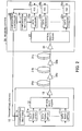
- FIG. 1 schematically illustrates an optical transmission system.
- the optical transmission system comprises a transmitting station 1, a receiving station 2, and a transmission path 3.
- the transmitting station 1 includes a transmitting-side distortion compensation coefficient storage 1a, a transmit signal processor 1b, and a transmitter 1c.
- the transmitting-side distortion compensation coefficient storage 1a stores transmitting-side distortion compensation coefficients for compensating for waveform distortion of an optical signal transmitted from the transmitting station 1 to the receiving station 2.
- the transmit signal processor 1b performs distortion compensation on the optical signal based on a transmitting-side distortion compensation coefficient stored in the transmitting-side distortion compensation coefficient storage 1a.
- the transmitter 1c outputs, to the transmission path 3, the optical signal to which the transmitting-side distortion compensation coefficient has been applied by the transmit signal processor 1b.
- the receiving-side distortion compensation coefficient storage 2b stores receiving-side distortion compensation coefficients for compensating for waveform distortion of the optical signal received by the receiver 2a.
- the received signal processor 2c performs distortion compensation on the optical signal received by the receiver 2a, based on a receiving-side distortion compensation coefficient stored in the receiving-side distortion compensation coefficient storage 2b.
- waveform distortion of the transmitted optical signal is complementarily compensated at the transmitting and receiving stations 1 and 2. Since the amount of compensation for waveform distortion of the optical signal can be shared between the transmitting and receiving stations 1 and 2, the waveform distortion can be efficiently reduced.
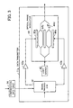
- FIG. 2 illustrates an optical transmission system according to the first embodiment.
- a transmitting station 10 transmits an optical signal
- a receiving station 20 receives the optical signal.
- the transmitting and receiving stations 10 and 20 are connected to each other by optical fibers 31a, 31b and 31c and repeaters 32a and 32b.
- the transmitting and receiving stations 10 and 20 share in the compensation for SPM-GVD induced distortion caused on the transmission path constituted by the optical fibers 31a, 31b and 31c and the repeaters 32a and 32b.
- the transmitting station 10 performs distortion compensation covering 70% of the transmission path
- the receiving station 20 performs distortion compensation covering the remaining 30%.
- the share ratio (relative amounts) of dispersion compensation is adjusted by looking up the quality of the signal received by the receiving station 20. This is because in the case of a transmission path with large nonlinear degradation, the signal quality can be effectively improved by decreasing the amount of dispersion compensation performed at the transmitting side and thereby reducing the dispersion compensation-induced distortion of the signal waveform prior to transmission over the transmission path. Also, when the system is upgraded to increase the number of channels, for example, there is a possibility that the optical power per signal changes, possibly making it necessary to change the compensation sharing ratio between the transmitting and receiving stations 10 and 20.
- the transmitting station 10 includes data transmitters 11a, 11b, ..., 11n, an optical multiplexer 12, an optical amplifier 13, and a compensation information table 14.
- the optical power is varied to each nominal value (typical value in design, standard set value) of 80%, 85%, 90%, 95%, 100%, 105%, 110%, 115% and 120%, and with respect to each optical power level, compensation coefficients are calculated for distances 30%, 35%, 40%, 45%, 50%, 55%, 60%, 65% and 70% from the transmitting station 10, the calculated compensation coefficients being stored in the compensation information table 14.
- nominal value typically value in design, standard set value
- the received signal transmitted with the nominal 95% optical power and received at the 30% distance of the transmission path for example, can be derived by transmission simulation as 95%,30% C[E(t)].
- compensation coefficients C -1 [] for the different optical power levels and the different transmission path lengths are obtained and stored in the compensation information table 14.
- the optical fibers 31a, 31b and 31c transmit the optical signal therethrough.
- the repeaters 32a and 32b amplify the optical signal that has attenuated while traveling through the respective optical fibers 31a, 31b and 31c.
- the receiving station 20 includes an optical amplifier 21, an optical demultiplexer 22, data receivers 23a, 23b, ..., 23n, a compensation information table 24, FEC (Forward Error Correction) units 25a, 25b, ..., 25n, and a compensation controller 26.
- the optical amplifier 21 amplifies the optical signal received from the optical fiber 31c, and outputs the amplified optical signal to the optical demultiplexer 22.
- the optical demultiplexer 22 demultiplexes the wavelength division-multiplexed optical signal into respective wavelengths, and outputs the demultiplexed optical signals to the respective data receivers 23a, 23b, ..., 23n.
- Each of the data receivers 23a, 23b, ..., 23n converts the corresponding demultiplexed optical signal to an electrical signal.
- the data receiver 23a When converting the optical signal to an electrical signal, the data receiver 23a carries out distortion compensation.
- the compensation information table 24 stores in advance compensation coefficients for compensating for distortion of the received signal. Using a suitable compensation coefficient stored in the compensation information table 24, the data receiver 23a performs distortion compensation on the received signal.
- a plurality of compensation coefficients for compensating for distortion of the received signal are previously stored in the compensation information table 24.
- Each compensation coefficient is calculated from the parameters including the transmit optical signal waveform, the optical power, the amount of dispersion, the nonlinear optical constant of the optical fibers, and the transmission path length, as stated above.
- multiple compensation coefficients are calculated in advance by varying the two parameters, namely, the optical power and the transmission path length, and the calculated compensation coefficients are stored in the compensation information table 24.
- the optical power is varied to each nominal value of 80%, 85%, 90%, 95%, 100%, 105%, 110%, 115% and 120%, and with respect to each optical power level, compensation coefficients are calculated for the remaining distances 70%, 65%, 60%, 55%, 50%, 45%, 40%, 35% and 30% to the receiving station 20, the calculated compensation coefficients being stored in the compensation information table 24.
- the transmit signal is E(t)
- the received signal transmitted with the nominal 95% optical power and received at the remaining 30% distance of the transmission path can be derived by the transmission simulation as 95%,30% C[E(t)].
- compensation coefficients C -1 [] for the different optical power levels and the different transmission path lengths are obtained and stored in the compensation information table 24.
- the transmit signal again undergoes a distortion of 95%,30% C[E(t)] during the transmission over the rest 30% distance of the transmission path
- the FEC units 25a, 25b, ..., 25n correct errors in the received electrical signals obtained through conversion by the respective data receivers 23a, 23b, ..., 23n.
- the FEC unit 25a outputs information on error correction, for example, bit error rate, to the compensation controller 26.
- the compensation controller 26 performs a control action such that the compensation coefficients are successively selected from among those stored in the compensation information tables 14 and 24 of the transmitting and receiving stations 10 and 20 and are output to the data transmitter 11a and the data receiver 23a, respectively.
- the compensation coefficient is calculated with respect to the different optical power levels because the nominal optical power and the optical power actually transmitted through the transmission path occasionally differ from each other. For this reason, the compensation coefficients calculated for the different optical power levels are applied to the optical signal to be transmitted, to find the compensation coefficient matching the actual optical power for transmission of the optical signal.
- FIG. 3 is a block diagram of the data transmitter. As illustrated, the data transmitter 11a includes a signal processor 41, amplifiers 42a and 42b, a light source 43, and an optical phase modulator 44. The compensation information table 14 is also shown in the figure.
- the signal processor 41 is input with digital data to be transmitted to the receiving station 20.
- the signal processor 41 separates the input digital data into I and Q signals, then applies the selected compensation coefficient in the compensation information table 14 to each of the signals (multiplies each signal by the compensation coefficient), and outputs the resulting signals to the respective amplifiers 42a and 42b.
- the amplifiers 42a and 42b amplify the respective signals output from the signal processor 41, and output the amplified signals to the optical phase modulator 44.
- the optical phase modulator 44 is also input (supplied) with light from the light source 43.
- the light source 43 comprises, for example, an LD (Laser Diode).
- the optical phase modulator 44 modulates the light from the light source 43 by means of the electrical signals output from the amplifiers 42a and 42b, and outputs the modulated signal.
- electrodes 44a and 44b constitute an I arm
- electrodes 44b and 44c constitute a Q arm
- a phase adjuster 44d adjusts the phase of the Q arm so that the Q arm may have a phase difference of 90° with respect to the I arm.
- FIG. 4 is a block diagram of the data receiver.
- the data receiver 23a includes an optical filter 51, a local light source 52, an optical 90° hybrid 53, balanced PDs (Photo Diodes) 54a and 54b, low-pass filters 55a and 55b, a signal processor 56, and a discrimination circuit 57.
- the compensation information table 24 is also shown in the figure.
- the optical filter 51 is input with the demultiplexed optical signal.
- the optical filter 51 removes noise (unwanted wavelengths) from the input optical signal and outputs the resulting signal to the optical 90° hybrid 53.
- the optical 90° hybrid 53 is formed using LiNbO 3 , for example, and has therein a port for directly outputting the optical signal and a port for outputting the optical signal with its phase shifted by 90°. Also, the optical 90° hybrid 53 has a port for directly outputting light from the local light source 52 and a port for outputting the local light with its phase shifted by 90°. The optical 90° hybrid 53 combines the directly output optical signal with the directly output local light 52 and outputs the combined optical signal to the balanced PD 54a. Also, the optical 90° hybrid 53 combines the optical signal and the local light 52, both shifted in phase by 90°, and outputs the combined optical signal to the balanced PD 54b.
- the balanced PD 54a converts the optical signal output from the optical 90° hybrid 53 to an electrical signal and outputs the obtained signal as the I signal.
- the balanced PD 54b converts the optical signal output from the optical 90° hybrid 53 to an electrical signal and outputs the obtained signal as the Q signal.
- the low-pass filters 55a and 55b respectively remove high-frequency components from the I and Q signals output from the balanced PDs 54a and 54b, and output the resulting signals to the signal processor 56.
- the signal processor 56 applies the selected compensation coefficient in the compensation information table 24 to each of the I and Q signals output from the respective low-pass filters 55a and 55b, and outputs the resulting signals to the discrimination circuit 57.
- the discrimination circuit 57 is provided with CDR (Clock Data Recovery), for example, and recovers the digital data that the transmitting station 10 has transmitted, from the I and Q signals output from the signal processor 56.
- CDR Lock Data Recovery
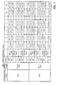
- FIG. 5 shows an exemplary data structure of the compensation information table in the transmitting station.
- the compensation coefficient is a complex number and carries two items of compensation information, namely, amplitude compensation data and phase compensation data.
- FIG. 5 shows only part of the data held by the compensation information table 14 in the transmitting station 10, that is, the compensation coefficient applied when the compensation ratio is 70:30 (70% distance from the transmitting station 10) and the optical power is at the nominal 100%, and the compensation coefficient applied when the compensation ratio is 70:30 and the optical power is at the nominal 105%.
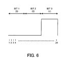
- Distortion compensation is carried out for every 3-bit block of the I and Q signals (hereinafter transmit signal), and the 3-bit transmit signal block is allotted amplitude compensation data "ai,j,k,l” and phase compensation data "bi,j,k,l".
- the compensation information table 14 exemplified in FIG. 5 one bit is divided into eight parts for the purpose of compensation, and therefore, the 3-bit transmit signal block is allotted 24 items of compensation data.
- i represents the type of compensation ratio
- j represents the type of optical power
- 1 indicates that the compensation data is for the nominal 100% optical power
- 2 indicates that the compensation data is for the nominal 105% optical power
- Symbol “k” represents the type of bit pattern of the transmit signal. Since, in the illustrated example, the distortion compensation is performed with respect to every 3-bit block of the transmit signal, there exist seven types as the bit patterns of the 3-bit transmit signal block whose distortion is to be compensated. Specifically, “1” indicates that the compensation data is for the transmit signal with the bit pattern "000”, “2” indicates that the compensation data is for the transmit signal with the bit pattern "001", and so on.
- FIG. 6 illustrates distortion compensation, wherein a waveform with the bit pattern "001" is shown as an example of the transmit signal whose distortion is to be compensated.
- the distortion compensation is carried out with respect to every 3-bit block of the transmit signal, as stated above.
- the 3-bit signal block is divided into 24 parts, and the thus-divided signal values are individually multiplied by the amplitude compensation data and the phase compensation data.
- the compensation information table 14 may be so configured as to hold compensation coefficients applicable to such a longer bit pattern.
- FIG. 7 shows an exemplary data structure of the compensation information table in the receiving station.
- the compensation information table 24 in the receiving station 20 holds compensation data similar to that stored in the counterpart in the transmitting station 10, and therefore, detailed description thereof is omitted.
- the amplitude compensation data is shown as "mi,j,k,l" and the phase compensation data as "ni,j,k,l".
- the received I and Q signals (hereinafter the received signal) have pattern dependence.
- the signal processor 56 of the receiving station 20 temporarily stores the received signal equivalent to three bits, for example, and applies, to the received signal, all patterns of the compensation coefficients corresponding to the compensation ratio and optical power instructed from the compensation controller 26 (the received signal is multiplied by each of the compensation coefficients). Then, the most likely signal pattern (signal pattern "0", "1" with maximum likelihood as the received signal) is output to the discrimination circuit 57.
- the compensation data is applied to every 3-bit block of the received signal.
- the compensation information table 24 may be so configured as to hold compensation coefficients applicable to such a longer bit pattern.
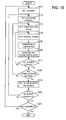
- FIG. 8 is a flowchart illustrating operation of the optical transmission system. The process explained below with reference to individual steps is executed when the optical transmission system is installed or upgraded or at regular intervals of time.
- Step S1 is executed following the branching Step S6, the compensation controller 26 sets a compensation ratio different from the previously selected one.
- Step S3 the signal processors 41 and 56 compensate for distortion of the signal by using the compensation coefficients set in Steps S1 and S2.
- Step S4 the compensation controller 26 stores the error rate output from the FEC unit 25a, along with the optical power level and compensation ratio then selected, in a storage device such as RAM (Random Access Memory) .
- a storage device such as RAM (Random Access Memory)
- Step S5 the compensation controller 26 determines whether or not the error rate has been measured with respect to all optical power levels. If the error rate has not yet been measured with respect to all optical power levels, the process proceeds to Step S2. If the error rate has been detected for all optical power levels, the process proceeds to Step S6.
- Step S7 the compensation controller 26 identifies the optical power and compensation ratio that provide the least error rate, from among those stored in the storage device.
- the compensation controller 26 then controls the compensation information tables 14 and 24 such that distortion of the signal is compensated with the use of the compensation coefficients corresponding to the identified optical power and compensation ratio.
- the transmitting and receiving stations 10 and 20 complementarily compensate for SPM-GVD induced distortion, whereby waveform distortion can be significantly reduced.
- each channel is provided with the compensation information tables and the compensation controller, like the data transmitter 11a and the data receiver 23a.
- the compensation controller 26 is provided in the receiving station 20 but may alternatively be provided in the transmitting station 10.
- control signal from the compensation controller 26 is transmitted to the transmitting station 10 via a route different from the transmission path constituted by the optical fibers 31a, 31b and 31c and the repeaters 32a and 32b.
- control signal may be transmitted through the transmission path constituted by the optical fibers 31a, 31b and 31c and the repeaters 32a and 32b.
- the compensation data tables are looked up to apply the compensation coefficients.
- the signal processors may be configured to calculate compensation data from the parameters including the transmit optical signal waveform, the optical power, the amount of dispersion, the nonlinear optical constant of the optical fibers, and the system length (transmission path length).
- FIG. 9 illustrates an optical transmission system according to the second embodiment.
- like reference numerals refer to like elements also appearing in FIG. 2 , and description of such elements is omitted.
- the optical fibers 31a, 31b and 31c and the repeaters 32a and 32b shown in FIG. 2 are omitted.
- a compensation information table 61 holds compensation data for compensating for distortion of the signal waveform of the data transmitter 11a caused under the influence of the signal input to the channel (data transmitter 11b) adjacent to the data transmitter 11a.
- the compensation information table 61 stores amplitude compensation data and phase compensation data that are used to compensate for distortion of the signal waveform of the data transmitter 11a when the signal input to the data transmitter 11b, which is the channel adjacent to the data transmitter 11a, is "000".
- the compensation information table 61 stores amplitude compensation data and phase compensation data that are used to compensate for distortion of the signal waveform of the data transmitter 11a when the signal input to the data transmitter 11b is "001", “010", ..., and "111". These items of compensation data are stored with respect to each compensation ratio and each optical power level, as in the compensation information table 14 shown in FIG. 5 .
- the expression a-b C -1 [] represents the compensation coefficient calculated for the signal on the channel "a" taking account of the influence of the signal on the channel "b".
- the data transmitters 11a, 11b, ..., 11n be channels 1, 2, ..., n, respectively.
- the compensation information table 61 in FIG. 9 stores the compensation coefficient 1-2 C -1 [] calculated for the signal on the channel 1 taking account of the influence of the signal on the channel 2.
- the channel 2 is the only channel that is adjacent to the channel 1.
- the channel n has only one adjacent channel, namely, the channel n-1.
- Each of the other channels has two adjacent channels.
- the channels 1 and 3 are adjacent to the channel 2.
- compensation coefficients 2-1 C -1 [] and 2-3 C -1 [] are stored in the compensation information table 61.
- the data transmitter 11b performs distortion compensation ( 2-1 C -1 [] + 2-3 C -1 []) ⁇ (E(t)) on the data and then transmits the resulting data to the receiving station 20.
- a compensation information table 62 stores the compensation coefficient 1-2 C -1 [].
- the data receiver 23a applies the compensation coefficient 1-2 C -1 [] to the received signal to thereby compensate for distortion.
- the compensation adjustment is successively carried out in the order: P(1,2), P(2,1), P(2,3), P(3,2), P(3,4), ..., P(N,N+1), and P(N+1,N).
- FIG. 10 is a flowchart illustrating operation of the optical transmission system.
- XPM-GVD is dependent on the state of polarization relative to adjacent channels and thus varies with time. Accordingly, the process explained below with reference to individual steps is executed in the transmitting and receiving stations 10 and 20 at regular intervals of time.
- Step S11 the compensation controller 26 selects a channel whose XPM-GVD distortion compensation is to be adjusted. For example, the channel 1 is selected first. Where Step S11 is executed again following the branching Step S21, the channel to be selected is changed to the channel 2, the channel 3, and so on.
- Step S12 the compensation controller 26 selects an adjacent channel from among those set in the compensation information tables 61 and 62. For example, where the channel 1 has been set, the compensation coefficient associated with the adjacent channel 2 is selected, and where the channel 2 has been set, the compensation coefficients associated with the adjacent channels 1 and 3 are selected.
- the compensation controller 26 selects a compensation ratio from among those set in the compensation information tables 61 and 62.
- the compensation ratio is set which specifies that the distance from the transmitting station 10 and the distance to the receiving station 20 are both 50%.
- Step S14 the compensation controller 26 selects an optical power level from among those set in the compensation information tables 61 and 62. For example, the nominal 100% optical power is selected.
- Step S14 is executed following the branching Step S17, the compensation controller 26 sets an optical power level different from the previously selected one.
- Step S17 the compensation controller 26 determines whether or not the error rate has been measured with respect to all optical power levels. If the error rate has not yet been measured with respect to all optical power levels, the process proceeds to Step S14. If the error rate has been detected for all optical power levels, the process proceeds to Step S18.
- Step S18 the compensation controller 26 determines whether or not the error rate has been measured with respect to all compensation ratios. If the error rate has not yet been measured with respect to all compensation ratios, the process proceeds to Step S13. If the error rate has been measured with respect to all compensation ratios, the process proceeds to Step S19.
- Step S19 the compensation controller 26 identifies the optical power and compensation ratio that provide the least error rate, from among those stored in the storage device.
- the compensation controller 26 then controls the compensation information tables 61 and 62 such that distortion of the signal is compensated with the use of the compensation coefficients corresponding to the identified optical power and compensation ratio.
- Step S21 the compensation controller 26 determines whether or not the adjustment has been carried out with respect to all channels. If the adjustment of all channels has not yet been completed, the process proceeds to Step S11; if the adjustment of all channels has been completed, the process ends.
- the transmitting and receiving stations 10 and 20 complementarily compensate for XPM-GVD induced distortion, whereby waveform distortion can be significantly reduced.
- the compensation information tables 61 and 62 individually store the distortion compensation coefficients 3-1 C -1 [], 3-2 C -1 , 3-4 C -1 [] and 3-5 C -1 , and the sum of the compensation coefficients, 3-1 C -1 [] + 3-2 C -1 + 3-4 C -1 [] + 3-5 C -1 , is applied to the signal.
- the compensation data tables are looked up to apply the compensation coefficients.
- the signal processors may be configured to calculate compensation data from the parameters including the transmit optical signal waveform, the optical power, the amount of dispersion, the nonlinear optical constant of the optical fibers, and the system length (transmission path length).
- the distortion compensations of the first and second embodiments are also possible.
- adjustment is made for both the SPM-GVD and XPM-GVD compensations.
- the adjustment may be periodically performed.
- the SPM-GVD and XPM-GVD compensation adjustments may be made with respect to the corresponding channels.
- FIG. 11 illustrates an optical transmission system according to the third embodiment.
- like reference numerals refer to like elements also appearing in FIG. 2 , and description of such elements is omitted.
- the optical fibers 31a, 31b and 31c and the repeaters 32a and 32b shown in FIG. 2 are omitted.
- the polarization separator 72 separates the demultiplexed optical signal from the optical demultiplexer 22 into respective polarization signals.
- the polarization separator 72 comprises, for example, a ⁇ /4 plate and a ⁇ /2 plate.
- the polarization separator 72 may be constituted by a Faraday rotator.
- the thus-separated optical polarization signals are output to the respective data receivers 23a and 23b, where the original data is recovered by demodulation.
- the optical signals from the data transmitters 11a and 11b are subjected to polarization division multiplexing, but the optical signals from the other data transmitters may also be similarly subjected to polarization division multiplexing by using polarization combiners 71, like the data transmitters 11a and 11b.
- the other data receivers than the data receivers 23a and 23b in the receiving station 20 are associated with polarization separators 72 each adapted to separate the optical signal into respective polarization signals.
- Whether the received polarization signal is a required one or not may be determined on the basis of frame information.
- a low-frequency signal may be superimposed on the intensity of the optical signal, and at the receiving side, the superimposed signal may be detected for the purpose of discrimination.
- polarization division multiplexing is applied to the optical transmission system of the first embodiment but is equally applicable to the optical transmission system of the second embodiment. Further, polarization division multiplexing can be applied to an optical transmission system constructed by combining the optical transmission systems of the first and second embodiments.
- waveform distortion of optical signals can be efficiently compensated.
Landscapes
- Physics & Mathematics (AREA)
- Electromagnetism (AREA)
- Engineering & Computer Science (AREA)
- Computer Networks & Wireless Communication (AREA)
- Signal Processing (AREA)
- Optical Communication System (AREA)
- Optical Modulation, Optical Deflection, Nonlinear Optics, Optical Demodulation, Optical Logic Elements (AREA)
Applications Claiming Priority (1)
| Application Number | Priority Date | Filing Date | Title |
|---|---|---|---|
| JP2008082310A JP5181770B2 (ja) | 2008-03-27 | 2008-03-27 | 光伝送システム |
Publications (2)
| Publication Number | Publication Date |
|---|---|
| EP2106044A1 true EP2106044A1 (fr) | 2009-09-30 |
| EP2106044B1 EP2106044B1 (fr) | 2013-02-27 |
Family
ID=40756211
Family Applications (1)
| Application Number | Title | Priority Date | Filing Date |
|---|---|---|---|
| EP08168230A Not-in-force EP2106044B1 (fr) | 2008-03-27 | 2008-11-04 | Système de transmission optique avec pré-compensation et post-compensation de la distorsion de la forme d'onde |
Country Status (3)
| Country | Link |
|---|---|
| US (1) | US8270843B2 (fr) |
| EP (1) | EP2106044B1 (fr) |
| JP (1) | JP5181770B2 (fr) |
Cited By (5)
| Publication number | Priority date | Publication date | Assignee | Title |
|---|---|---|---|---|
| EP2362556A1 (fr) * | 2010-02-19 | 2011-08-31 | ADVA AG Optical Networking | Procédé et système doté de compensation de distorsion |
| EP2434668A1 (fr) * | 2010-09-28 | 2012-03-28 | Fujitsu Limited | Appareil de compensation non linéaire et transmetteur |
| CN102655433A (zh) * | 2011-03-04 | 2012-09-05 | 富士通株式会社 | 非线性损伤补偿方法和装置 |
| EP2770649A4 (fr) * | 2011-10-20 | 2015-08-05 | Mitsubishi Electric Corp | Émetteur optique précorrigé et procédé d'émission optique précorrigée |
| EP2866362A3 (fr) * | 2013-10-14 | 2015-08-26 | Korea Advanced Institute of Science and Technology | Compensation de dispersion électronique pour laser modulé à retour-direct réparti de faible coût |
Families Citing this family (56)
| Publication number | Priority date | Publication date | Assignee | Title |
|---|---|---|---|---|
| JP5476697B2 (ja) | 2008-09-26 | 2014-04-23 | 富士通株式会社 | 光信号送信装置 |
| US8326159B2 (en) * | 2009-03-20 | 2012-12-04 | University Of Central Florida Research Foundation, Inc. | Electronic compensation of impairments using wavelet filters for backward propagation |
| WO2010140289A1 (fr) * | 2009-06-05 | 2010-12-09 | 日本電気株式会社 | Système de communication optique, son récepteur optique et son procédé de communication optique |
| CN102754367B (zh) | 2009-10-07 | 2016-06-15 | 奥菲迪乌姆有限公司 | 光通信链路中的多信道非线性补偿 |
| JP5375519B2 (ja) * | 2009-10-26 | 2013-12-25 | 富士通株式会社 | 非線形歪検出回路、光受信機、光伝送システム、および非線形歪検出方法 |
| JP5614126B2 (ja) * | 2010-06-28 | 2014-10-29 | 富士通株式会社 | 伝送装置及び伝送システム |
| JP5760419B2 (ja) * | 2010-12-13 | 2015-08-12 | 富士通株式会社 | 光送信装置および光送信方法 |
| CN102655432B (zh) * | 2011-03-04 | 2015-08-26 | 富士通株式会社 | 非线性损伤补偿方法和装置 |
| EP2506478A1 (fr) * | 2011-03-25 | 2012-10-03 | Alcatel Lucent | Procédé de transmission optique de données utilisant le multiplexage de division de polarisation |
| WO2011157128A2 (fr) * | 2011-05-31 | 2011-12-22 | 华为技术有限公司 | Procédé et dispositif de traitement de signaux optiques |
| EP2645599B1 (fr) * | 2012-03-29 | 2015-08-19 | Alcatel Lucent | Optimisation souple du rapport signal sur bruit pour des systèmes WDM cohérents très denses |
| JP5991210B2 (ja) * | 2012-03-29 | 2016-09-14 | 富士通株式会社 | 光信号送信装置 |
| EP2804334A1 (fr) * | 2013-05-13 | 2014-11-19 | Xieon Networks S.à.r.l. | Procédé, dispositif et système de communication pour la réduction des dégradations de transmission optique |
| US9160456B2 (en) * | 2013-09-20 | 2015-10-13 | Alcatel Lucent | Dispersion management for inhomogeneous fiber-optic links |
| JP6281387B2 (ja) * | 2014-04-07 | 2018-02-21 | 富士通株式会社 | デジタルコヒーレント受信器および受信方法 |
| US9571198B2 (en) * | 2014-07-25 | 2017-02-14 | Futurewei Technologies, Inc. | Compensation of non-linear transmitter impairments in optical communication networks |
| JP2016072696A (ja) * | 2014-09-26 | 2016-05-09 | 富士通株式会社 | 歪み補償装置及び歪み補償方法 |
| US9590730B2 (en) | 2014-10-01 | 2017-03-07 | Futurewei Technologies, Inc. | Optical transmitter with optical receiver-specific dispersion pre-compensation |
| US10070206B2 (en) * | 2014-12-30 | 2018-09-04 | Infinera Corporation | Reduction of wavelength selective switch (WSS) filter-based impairment using differentiated channel modulation formats |
| JP6492827B2 (ja) * | 2015-03-19 | 2019-04-03 | 富士通株式会社 | 光受信器および光受信方法 |
| JP2016213729A (ja) * | 2015-05-12 | 2016-12-15 | 富士通株式会社 | 光送信装置および光受信装置 |
| FI4002724T3 (fi) | 2015-12-13 | 2025-09-30 | Gxc Llc | Häiriönpoistomenetelmiä ja -laite |
| JP6759742B2 (ja) * | 2016-06-16 | 2020-09-23 | 富士通株式会社 | 受信装置及び設定方法 |
| JP2018007058A (ja) * | 2016-07-04 | 2018-01-11 | 富士通株式会社 | ネットワーク制御装置、光伝送システムおよび障害判定方法 |
| US10257746B2 (en) | 2016-07-16 | 2019-04-09 | GenXComm, Inc. | Interference cancellation methods and apparatus |
| JP6633470B2 (ja) * | 2016-07-28 | 2020-01-22 | 日本電信電話株式会社 | 光送信機、光受信機及び光送受信機 |
| US10020886B2 (en) * | 2016-10-17 | 2018-07-10 | Panduit Corp. | Methods and systems for fiber optic communication |
| US10887022B2 (en) * | 2017-06-15 | 2021-01-05 | Nokia Of America Corporation | Backward propagation with compensation of some nonlinear effects of polarization mode dispersion |
| JP2019009647A (ja) * | 2017-06-26 | 2019-01-17 | 富士通株式会社 | 送信装置、受信装置及び推定方法 |
| US11150409B2 (en) | 2018-12-27 | 2021-10-19 | GenXComm, Inc. | Saw assisted facet etch dicing |
| US10742326B1 (en) | 2019-04-18 | 2020-08-11 | Microsoft Technology Licensing, Llc | Power-based encoding of data to be transmitted over an optical communication path |
| US10998982B2 (en) | 2019-04-18 | 2021-05-04 | Microsoft Technology Licensing, Llc | Transmitter for throughput increases for optical communications |
| US10873392B2 (en) | 2019-04-18 | 2020-12-22 | Microsoft Technology Licensing, Llc | Throughput increases for optical communications |
| US10756817B1 (en) | 2019-04-18 | 2020-08-25 | Microsoft Technology Licensing, Llc | Power switching for systems implementing throughput improvements for optical communications |
| US10873393B2 (en) | 2019-04-18 | 2020-12-22 | Microsoft Technology Licensing, Llc | Receiver training for throughput increases in optical communications |
| US10938485B2 (en) | 2019-04-18 | 2021-03-02 | Microsoft Technology Licensing, Llc | Error control coding with dynamic ranges |
| US10951342B2 (en) | 2019-04-18 | 2021-03-16 | Microsoft Technology Licensing, Llc | Throughput increases for optical communications |
| US10911155B2 (en) | 2019-04-18 | 2021-02-02 | Microsoft Technology Licensing, Llc | System for throughput increases for optical communications |
| US10911152B2 (en) * | 2019-04-18 | 2021-02-02 | Microsoft Technology Licensing, Llc | Power-based decoding of data received over an optical communication path |
| US11018776B2 (en) | 2019-04-18 | 2021-05-25 | Microsoft Technology Licensing, Llc | Power-based decoding of data received over an optical communication path |
| US10897315B2 (en) * | 2019-04-18 | 2021-01-19 | Microsoft Technology Licensing, Llc | Power-based decoding of data received over an optical communication path |
| US10862591B1 (en) | 2019-04-18 | 2020-12-08 | Microsoft Technology Licensing, Llc | Unequal decision regions for throughput increases for optical communications |
| US10742325B1 (en) | 2019-04-18 | 2020-08-11 | Microsoft Technology Licensing, Llc | Power-based encoding of data to be transmitted over an optical communication path |
| US10892847B2 (en) | 2019-04-18 | 2021-01-12 | Microsoft Technology Licensing, Llc | Blind detection model optimization |
| US10727945B1 (en) | 2019-07-15 | 2020-07-28 | GenXComm, Inc. | Efficiently combining multiple taps of an optical filter |
| US10911141B1 (en) | 2019-07-30 | 2021-02-02 | Microsoft Technology Licensing, Llc | Dynamically selecting a channel model for optical communications |
| US11215755B2 (en) | 2019-09-19 | 2022-01-04 | GenXComm, Inc. | Low loss, polarization-independent, large bandwidth mode converter for edge coupling |
| US11539394B2 (en) | 2019-10-29 | 2022-12-27 | GenXComm, Inc. | Self-interference mitigation in in-band full-duplex communication systems |
| US11796737B2 (en) | 2020-08-10 | 2023-10-24 | GenXComm, Inc. | Co-manufacturing of silicon-on-insulator waveguides and silicon nitride waveguides for hybrid photonic integrated circuits |
| US12001065B1 (en) | 2020-11-12 | 2024-06-04 | ORCA Computing Limited | Photonics package with tunable liquid crystal lens |
| WO2022176039A1 (fr) * | 2021-02-17 | 2022-08-25 | 日本電信電話株式会社 | Dispositif et procédé de réception |
| WO2022178182A1 (fr) | 2021-02-18 | 2022-08-25 | GenXComm, Inc. | Maximisation de l'efficacité de systèmes de communication avec des sous-systèmes d'annulation d'auto-interférences |
| EP4331120A1 (fr) | 2021-04-29 | 2024-03-06 | Genxcomm, Inc. | Sous-systèmes d'annulation d'auto-interférence pour noeuds de réseau maillé |
| US11838056B2 (en) | 2021-10-25 | 2023-12-05 | GenXComm, Inc. | Hybrid photonic integrated circuits for ultra-low phase noise signal generators |
| JP7755152B2 (ja) * | 2021-12-22 | 2025-10-16 | 富士通株式会社 | 光送受信システム、光送信装置、及び光受信装置 |
| CN119210587A (zh) * | 2023-06-26 | 2024-12-27 | 华为技术有限公司 | 一种方法、系统和相关设备 |
Citations (7)
| Publication number | Priority date | Publication date | Assignee | Title |
|---|---|---|---|---|
| EP0700178A2 (fr) * | 1994-08-02 | 1996-03-06 | Fujitsu Limited | Système de transmission optique avec optimisation des conditions de transmission |
| US20030081292A1 (en) * | 2001-10-30 | 2003-05-01 | Fujitsu Limited | Transmission characteristic compensation control system |
| US20050047802A1 (en) * | 2003-09-02 | 2005-03-03 | Harris Corporation | Post-detection, fiber optic dispersion compensation using adjustable infinite impulse response filter employing trained or decision-directed adaptation |
| US20050185964A1 (en) * | 1997-09-09 | 2005-08-25 | Fujitsu Limited | Dispersion compensation apparatus including a fixed dispersion compensator for coarse compensation and a variable dispersion compensator for fine compensation |
| US20050226631A1 (en) * | 2004-04-09 | 2005-10-13 | Sandy Thomson | Dispersion compensation in optical systems |
| JP2006522508A (ja) | 2003-04-03 | 2006-09-28 | ノーテル・ネットワークス・リミテッド | 光通信システムにおける非線形効果の電気的領域補償 |
| EP1855399A1 (fr) * | 2006-05-08 | 2007-11-14 | Alcatel Lucent | Procédé de fonctionnement et d'optimisation d'un système de transmission multiplexé en longueurs d'onde et produit de programme informatique correspondant |
Family Cites Families (17)
| Publication number | Priority date | Publication date | Assignee | Title |
|---|---|---|---|---|
| JP3522044B2 (ja) * | 1996-04-19 | 2004-04-26 | 富士通株式会社 | 光伝送システム |
| JP4063908B2 (ja) * | 1997-01-29 | 2008-03-19 | 富士通株式会社 | 光源装置、光増幅器及び光通信システム |
| US6574389B1 (en) * | 1999-05-24 | 2003-06-03 | Broadband Royalty | Optical communication with pre-compensation for odd order distortion in modulation and transmission |
| US6580535B1 (en) * | 1999-12-28 | 2003-06-17 | Telefonaktiebolaget Lm Ericsson (Publ) | Polarization division multiplexing in optical data transmission systems |
| JP4671478B2 (ja) * | 2000-08-08 | 2011-04-20 | 富士通株式会社 | 波長多重光通信システムおよび波長多重光通信方法 |
| JP4011290B2 (ja) * | 2001-01-10 | 2007-11-21 | 富士通株式会社 | 分散補償方法、分散補償装置および光伝送システム |
| JP4686906B2 (ja) * | 2001-06-04 | 2011-05-25 | 株式会社日立製作所 | 波長多重用光伝送装置 |
| US20030090768A1 (en) * | 2001-08-01 | 2003-05-15 | Xiang Liu | Long haul optical communication system |
| JP2003169037A (ja) * | 2001-11-29 | 2003-06-13 | Nec Corp | 波長多重伝送装置 |
| US7382984B2 (en) * | 2002-10-03 | 2008-06-03 | Nortel Networks Limited | Electrical domain compensation of optical dispersion in an optical communications system |
| JP4491268B2 (ja) * | 2004-04-21 | 2010-06-30 | 富士通株式会社 | 分散補償量設定方法,受信端局および波長多重光伝送システム |
| JP4479496B2 (ja) * | 2004-12-15 | 2010-06-09 | 日本電気株式会社 | 波形歪み補償装置、波形歪み補償システムおよび波形歪み補償方法 |
| JP4686370B2 (ja) * | 2006-01-30 | 2011-05-25 | 株式会社日立製作所 | Wdm伝送システム |
| CN101207445A (zh) * | 2006-12-21 | 2008-06-25 | 华为技术有限公司 | 一种色散补偿方法和光纤传输系统 |
| JP5188194B2 (ja) * | 2008-02-07 | 2013-04-24 | 三菱電機株式会社 | 送受信システム |
| JP5080349B2 (ja) * | 2008-04-28 | 2012-11-21 | 株式会社アドバンテスト | アナログデジタル変換装置、アナログデジタル変換方法、試験装置、および、プログラム |
| JP2010004251A (ja) * | 2008-06-19 | 2010-01-07 | Hitachi Communication Technologies Ltd | 光伝送装置および光伝送方法 |
-
2008
- 2008-03-27 JP JP2008082310A patent/JP5181770B2/ja not_active Expired - Fee Related
- 2008-10-29 US US12/289,531 patent/US8270843B2/en not_active Expired - Fee Related
- 2008-11-04 EP EP08168230A patent/EP2106044B1/fr not_active Not-in-force
Patent Citations (7)
| Publication number | Priority date | Publication date | Assignee | Title |
|---|---|---|---|---|
| EP0700178A2 (fr) * | 1994-08-02 | 1996-03-06 | Fujitsu Limited | Système de transmission optique avec optimisation des conditions de transmission |
| US20050185964A1 (en) * | 1997-09-09 | 2005-08-25 | Fujitsu Limited | Dispersion compensation apparatus including a fixed dispersion compensator for coarse compensation and a variable dispersion compensator for fine compensation |
| US20030081292A1 (en) * | 2001-10-30 | 2003-05-01 | Fujitsu Limited | Transmission characteristic compensation control system |
| JP2006522508A (ja) | 2003-04-03 | 2006-09-28 | ノーテル・ネットワークス・リミテッド | 光通信システムにおける非線形効果の電気的領域補償 |
| US20050047802A1 (en) * | 2003-09-02 | 2005-03-03 | Harris Corporation | Post-detection, fiber optic dispersion compensation using adjustable infinite impulse response filter employing trained or decision-directed adaptation |
| US20050226631A1 (en) * | 2004-04-09 | 2005-10-13 | Sandy Thomson | Dispersion compensation in optical systems |
| EP1855399A1 (fr) * | 2006-05-08 | 2007-11-14 | Alcatel Lucent | Procédé de fonctionnement et d'optimisation d'un système de transmission multiplexé en longueurs d'onde et produit de programme informatique correspondant |
Non-Patent Citations (3)
| Title |
|---|
| "1.6 Gbit/s Real-Time Synchronous QPSK Transmission with Standard DFB Lasers", UNIVERSITY OF PADERBORN, ECOC, 2006 |
| ELECTRONIC DISPERSION COMPENSATION TOURNIQUETS FOR OPTICAL COMMUNICATIONS SYSTEMS, 2006 |
| MOON H ET AL: "FPGA-Based adaptive digital predistortion for radio-over-fiber links", MICROPROCESSORS AND MICROSYSTEMS, IPC BUSINESS PRESS LTD. LONDON, GB, vol. 30, no. 3, 5 May 2006 (2006-05-05), pages 145 - 154, XP025096249, ISSN: 0141-9331, [retrieved on 20060505] * |
Cited By (8)
| Publication number | Priority date | Publication date | Assignee | Title |
|---|---|---|---|---|
| EP2362556A1 (fr) * | 2010-02-19 | 2011-08-31 | ADVA AG Optical Networking | Procédé et système doté de compensation de distorsion |
| US8755694B2 (en) | 2010-02-19 | 2014-06-17 | Adva Optical Networking Se | Method and a system with distortion compensation |
| EP2434668A1 (fr) * | 2010-09-28 | 2012-03-28 | Fujitsu Limited | Appareil de compensation non linéaire et transmetteur |
| CN102655433A (zh) * | 2011-03-04 | 2012-09-05 | 富士通株式会社 | 非线性损伤补偿方法和装置 |
| EP2495890A1 (fr) * | 2011-03-04 | 2012-09-05 | Fujitsu Limited | Procédé et appareil de compensation des dégâts non linaires |
| CN102655433B (zh) * | 2011-03-04 | 2016-03-30 | 富士通株式会社 | 非线性损伤补偿方法和装置 |
| EP2770649A4 (fr) * | 2011-10-20 | 2015-08-05 | Mitsubishi Electric Corp | Émetteur optique précorrigé et procédé d'émission optique précorrigée |
| EP2866362A3 (fr) * | 2013-10-14 | 2015-08-26 | Korea Advanced Institute of Science and Technology | Compensation de dispersion électronique pour laser modulé à retour-direct réparti de faible coût |
Also Published As
| Publication number | Publication date |
|---|---|
| JP5181770B2 (ja) | 2013-04-10 |
| US20090245809A1 (en) | 2009-10-01 |
| US8270843B2 (en) | 2012-09-18 |
| EP2106044B1 (fr) | 2013-02-27 |
| JP2009239555A (ja) | 2009-10-15 |
Similar Documents
| Publication | Publication Date | Title |
|---|---|---|
| EP2106044B1 (fr) | Système de transmission optique avec pré-compensation et post-compensation de la distorsion de la forme d'onde | |
| Yaman et al. | Nonlinear impairment compensation for polarization-division multiplexed WDM transmission using digital backward propagation | |
| Ono et al. | Characteristics of optical duobinary signals in terabit/s capacity, high-spectral efficiency WDM systems | |
| JP4592887B2 (ja) | 波長分散を補償する方法及びシステム | |
| EP1076434B1 (fr) | Dispositif et procédé d'amplification optique pour l'amplification de lumière d'une bande de longueur d'onde étendue | |
| US7058311B1 (en) | System and method for dispersion compensation in an optical communication system | |
| US8280258B2 (en) | Optical communication systems and methods utilizing a split amplification band and nonlinear compensation | |
| Yamazaki et al. | 100-Gb/s optical transport network and beyond employing digital signal processing | |
| US8712255B2 (en) | Optical receiver and optical transfer apparatus | |
| US7400830B2 (en) | Quality monitoring method and apparatus for wavelength division multiplexed optical signal and optical transmission system using the same | |
| US20030170028A1 (en) | Optical transmitter, optical repeater, optical receiver and optical transmission method | |
| US7310318B1 (en) | Method and system for using optical phase conjugation in an optical communications network | |
| US7376353B2 (en) | Method and apparatus for dispersion management in optical mesh networks | |
| EP2494716B1 (fr) | Compensation de dispersion distincte pour canaux cohérents et canaux non cohérents | |
| JP3352570B2 (ja) | 波長多重伝送方式の雑音抑圧方法 | |
| Jansen et al. | 16/spl times/40 gb/s over 800 km of SSMF using mid-link spectral inversion | |
| US20050095006A1 (en) | Cable station for an undersea optical transmission system | |
| US7039272B2 (en) | Optical transmission equipment with dispersion compensation, and dispersion compensating method | |
| Pastorelli et al. | Investigation of the dependence of non-linear interference on the number of WDM channels in coherent optical networks | |
| JP4056846B2 (ja) | 分散モニタ装置、分散モニタ方法および自動分散補償システム | |
| Chang et al. | Transmission of 112 Gb/s dual-carrier DQPSK signal over 10 Gb/s-based WDM optical links | |
| Xia et al. | 92-Gb/s field trial with ultra-high PMD tolerance of 107-ps DGD | |
| JPH10242941A (ja) | 光波長多重伝送装置 | |
| Chen et al. | Asymmetric DSM-DBP enabled 800 Gb/s PS-DP-64QAM Transmission over 2400 km SSMF | |
| Buchali et al. | Nonlinear limitations in a joint transmission of 100Gb/s O-OFDM and 40Gb/s DPSK over a 50 GHz channel grid |
Legal Events
| Date | Code | Title | Description |
|---|---|---|---|
| PUAI | Public reference made under article 153(3) epc to a published international application that has entered the european phase |
Free format text: ORIGINAL CODE: 0009012 |
|
| AK | Designated contracting states |
Kind code of ref document: A1 Designated state(s): AT BE BG CH CY CZ DE DK EE ES FI FR GB GR HR HU IE IS IT LI LT LU LV MC MT NL NO PL PT RO SE SI SK TR |
|
| AX | Request for extension of the european patent |
Extension state: AL BA MK RS |
|
| 17P | Request for examination filed |
Effective date: 20100329 |
|
| AKX | Designation fees paid |
Designated state(s): FR GB |
|
| REG | Reference to a national code |
Ref country code: DE Ref legal event code: 8566 |
|
| GRAP | Despatch of communication of intention to grant a patent |
Free format text: ORIGINAL CODE: EPIDOSNIGR1 |
|
| GRAS | Grant fee paid |
Free format text: ORIGINAL CODE: EPIDOSNIGR3 |
|
| REG | Reference to a national code |
Ref country code: DE Ref legal event code: R079 Free format text: PREVIOUS MAIN CLASS: H04B0010180000 Ipc: H04B0010250700 |
|
| GRAA | (expected) grant |
Free format text: ORIGINAL CODE: 0009210 |
|
| AK | Designated contracting states |
Kind code of ref document: B1 Designated state(s): FR GB |
|
| REG | Reference to a national code |
Ref country code: GB Ref legal event code: FG4D |
|
| RIC1 | Information provided on ipc code assigned before grant |
Ipc: H04B 10/2507 20130101AFI20130123BHEP |
|
| PLBE | No opposition filed within time limit |
Free format text: ORIGINAL CODE: 0009261 |
|
| STAA | Information on the status of an ep patent application or granted ep patent |
Free format text: STATUS: NO OPPOSITION FILED WITHIN TIME LIMIT |
|
| 26N | No opposition filed |
Effective date: 20131128 |
|
| REG | Reference to a national code |
Ref country code: FR Ref legal event code: PLFP Year of fee payment: 8 |
|
| REG | Reference to a national code |
Ref country code: FR Ref legal event code: PLFP Year of fee payment: 9 |
|
| PGFP | Annual fee paid to national office [announced via postgrant information from national office to epo] |
Ref country code: GB Payment date: 20161102 Year of fee payment: 9 Ref country code: FR Payment date: 20161014 Year of fee payment: 9 |
|
| GBPC | Gb: european patent ceased through non-payment of renewal fee |
Effective date: 20171104 |
|
| REG | Reference to a national code |
Ref country code: FR Ref legal event code: ST Effective date: 20180731 |
|
| PG25 | Lapsed in a contracting state [announced via postgrant information from national office to epo] |
Ref country code: FR Free format text: LAPSE BECAUSE OF NON-PAYMENT OF DUE FEES Effective date: 20171130 |
|
| PG25 | Lapsed in a contracting state [announced via postgrant information from national office to epo] |
Ref country code: GB Free format text: LAPSE BECAUSE OF NON-PAYMENT OF DUE FEES Effective date: 20171104 |