EP2107547A2 - Bildanzeigevorrichtung und Steuerverfahren dafür - Google Patents
Bildanzeigevorrichtung und Steuerverfahren dafür Download PDFInfo
- Publication number
- EP2107547A2 EP2107547A2 EP09156876A EP09156876A EP2107547A2 EP 2107547 A2 EP2107547 A2 EP 2107547A2 EP 09156876 A EP09156876 A EP 09156876A EP 09156876 A EP09156876 A EP 09156876A EP 2107547 A2 EP2107547 A2 EP 2107547A2
- Authority
- EP
- European Patent Office
- Prior art keywords
- waveform
- pulse
- modulated pulse
- outputting
- output
- Prior art date
- Legal status (The legal status is an assumption and is not a legal conclusion. Google has not performed a legal analysis and makes no representation as to the accuracy of the status listed.)
- Withdrawn
Links
- 238000000034 method Methods 0.000 title claims description 9
- 230000001965 increasing effect Effects 0.000 claims description 10
- 239000011159 matrix material Substances 0.000 claims description 9
- 230000007423 decrease Effects 0.000 claims 5
- 230000007704 transition Effects 0.000 abstract description 7
- 230000000630 rising effect Effects 0.000 description 28
- 238000006243 chemical reaction Methods 0.000 description 13
- 238000010586 diagram Methods 0.000 description 12
- 239000003086 colorant Substances 0.000 description 11
- 239000003990 capacitor Substances 0.000 description 6
- 238000010894 electron beam technology Methods 0.000 description 6
- 238000005070 sampling Methods 0.000 description 5
- 238000012886 linear function Methods 0.000 description 2
- 230000004048 modification Effects 0.000 description 2
- 238000012986 modification Methods 0.000 description 2
- OAICVXFJPJFONN-UHFFFAOYSA-N Phosphorus Chemical compound [P] OAICVXFJPJFONN-UHFFFAOYSA-N 0.000 description 1
- 230000008859 change Effects 0.000 description 1
- 230000003247 decreasing effect Effects 0.000 description 1
- 230000002708 enhancing effect Effects 0.000 description 1
- 239000004973 liquid crystal related substance Substances 0.000 description 1
- 230000004044 response Effects 0.000 description 1
Images


Classifications
-
- G—PHYSICS
- G09—EDUCATION; CRYPTOGRAPHY; DISPLAY; ADVERTISING; SEALS
- G09G—ARRANGEMENTS OR CIRCUITS FOR CONTROL OF INDICATING DEVICES USING STATIC MEANS TO PRESENT VARIABLE INFORMATION
- G09G3/00—Control arrangements or circuits, of interest only in connection with visual indicators other than cathode-ray tubes
- G09G3/20—Control arrangements or circuits, of interest only in connection with visual indicators other than cathode-ray tubes for presentation of an assembly of a number of characters, e.g. a page, by composing the assembly by combination of individual elements arranged in a matrix no fixed position being assigned to or needed to be assigned to the individual characters or partial characters
- G09G3/22—Control arrangements or circuits, of interest only in connection with visual indicators other than cathode-ray tubes for presentation of an assembly of a number of characters, e.g. a page, by composing the assembly by combination of individual elements arranged in a matrix no fixed position being assigned to or needed to be assigned to the individual characters or partial characters using controlled light sources
-
- G—PHYSICS
- G09—EDUCATION; CRYPTOGRAPHY; DISPLAY; ADVERTISING; SEALS
- G09G—ARRANGEMENTS OR CIRCUITS FOR CONTROL OF INDICATING DEVICES USING STATIC MEANS TO PRESENT VARIABLE INFORMATION
- G09G3/00—Control arrangements or circuits, of interest only in connection with visual indicators other than cathode-ray tubes
- G09G3/20—Control arrangements or circuits, of interest only in connection with visual indicators other than cathode-ray tubes for presentation of an assembly of a number of characters, e.g. a page, by composing the assembly by combination of individual elements arranged in a matrix no fixed position being assigned to or needed to be assigned to the individual characters or partial characters
- G09G3/2007—Display of intermediate tones
- G09G3/2077—Display of intermediate tones by a combination of two or more gradation control methods
- G09G3/2081—Display of intermediate tones by a combination of two or more gradation control methods with combination of amplitude modulation and time modulation
-
- G—PHYSICS
- G09—EDUCATION; CRYPTOGRAPHY; DISPLAY; ADVERTISING; SEALS
- G09G—ARRANGEMENTS OR CIRCUITS FOR CONTROL OF INDICATING DEVICES USING STATIC MEANS TO PRESENT VARIABLE INFORMATION
- G09G2310/00—Command of the display device
- G09G2310/02—Addressing, scanning or driving the display screen or processing steps related thereto
- G09G2310/0264—Details of driving circuits
- G09G2310/027—Details of drivers for data electrodes, the drivers handling digital grey scale data, e.g. use of D/A converters
-
- G—PHYSICS
- G09—EDUCATION; CRYPTOGRAPHY; DISPLAY; ADVERTISING; SEALS
- G09G—ARRANGEMENTS OR CIRCUITS FOR CONTROL OF INDICATING DEVICES USING STATIC MEANS TO PRESENT VARIABLE INFORMATION
- G09G2310/00—Command of the display device
- G09G2310/06—Details of flat display driving waveforms
- G09G2310/066—Waveforms comprising a gently increasing or decreasing portion, e.g. ramp
-
- G—PHYSICS
- G09—EDUCATION; CRYPTOGRAPHY; DISPLAY; ADVERTISING; SEALS
- G09G—ARRANGEMENTS OR CIRCUITS FOR CONTROL OF INDICATING DEVICES USING STATIC MEANS TO PRESENT VARIABLE INFORMATION
- G09G2320/00—Control of display operating conditions
- G09G2320/06—Adjustment of display parameters
- G09G2320/0666—Adjustment of display parameters for control of colour parameters, e.g. colour temperature
-
- G—PHYSICS
- G09—EDUCATION; CRYPTOGRAPHY; DISPLAY; ADVERTISING; SEALS
- G09G—ARRANGEMENTS OR CIRCUITS FOR CONTROL OF INDICATING DEVICES USING STATIC MEANS TO PRESENT VARIABLE INFORMATION
- G09G2330/00—Aspects of power supply; Aspects of display protection and defect management
- G09G2330/02—Details of power systems and of start or stop of display operation
- G09G2330/025—Reduction of instantaneous peaks of current
-
- G—PHYSICS
- G09—EDUCATION; CRYPTOGRAPHY; DISPLAY; ADVERTISING; SEALS
- G09G—ARRANGEMENTS OR CIRCUITS FOR CONTROL OF INDICATING DEVICES USING STATIC MEANS TO PRESENT VARIABLE INFORMATION
- G09G2330/00—Aspects of power supply; Aspects of display protection and defect management
- G09G2330/02—Details of power systems and of start or stop of display operation
- G09G2330/028—Generation of voltages supplied to electrode drivers in a matrix display other than LCD
-
- H—ELECTRICITY
- H03—ELECTRONIC CIRCUITRY
- H03K—PULSE TECHNIQUE
- H03K17/00—Electronic switching or gating, i.e. not by contact-making and –breaking
- H03K17/16—Modifications for eliminating interference voltages or currents
- H03K17/161—Modifications for eliminating interference voltages or currents in field-effect transistor switches
- H03K17/162—Modifications for eliminating interference voltages or currents in field-effect transistor switches without feedback from the output circuit to the control circuit
- H03K17/163—Soft switching
Definitions
- the present invention relates to an image display apparatus and a control method of the same.
- a display apparatus using an electron-emitting device such as a display apparatus using an electron-emitting device (electron beam display apparatus), a liquid crystal display apparatus, a plasma display apparatus, an organic EL display apparatus, and the like.
- This type of the image display apparatuses have a display panel (matrix panel), to which a lot of display devices are provided in a matrix pattern, and a drive circuit for driving the display devices.
- a modulation signal (modulated pulse), which is modulated according to an image signal, is supplied to a display device to be driven.
- a pulse width modulation, an amplitude modulation, and the like are known as a modulation system.
- Japanese Patent Application Laid-Open No. 2003-173159 discloses a modulation system using the pulse width modulation and the amplitude modulation in combination. Further, the document discloses a modulation circuit in which a pulse waveform rises and falls stepwise.
- Stepwise rising and falling of a pulse waveform could somewhat suppress disturbance (overshoot, ringing, and the like) of the waveform at a voltage transition, as disclosed in Japanese Patent Application Laid-Open No. 2003-173159 .
- a display panel is arranged to display a much finer image and to be driven at a higher speed, it is desired to further suppress disturbance of the waveform at a voltage transition for more stabilized drive of the display panel.
- a matrix drive type image display apparatus such as an electron beam display apparatus, since a matrix panel has a large capacity and its drive voltage is high, it is desired to reduce high-frequency components contained in a pulse waveform as much as possible.
- the present invention provides a technique for suppressing disturbance of a modulated pulse waveform at a voltage transition.
- the present invention employs the following constitution.
- the present invention in its first aspect provides an image display apparatus as specified in claims 1 to 9.
- the present invention in its second aspect provides a control method as specified in claims 10 to 12.
- disturbance of a modulated pulse waveform can be suppressed at a voltage transition.
- the present invention can be preferably applied to an image display apparatus having a display panel (matrix panel) to which a plurality of display devices are arranged in matrix with a plurality of column wires and a plurality of row wires.
- This type of the image display apparatus includes, for example, electron beam display apparatuses, plasma display apparatuses, organic EL display apparatuses, and the like.
- the present invention is preferably applied to electron beam display apparatuses since electron beam display apparatuses have a large wiring capacitance and a large device capacitance of a matrix panel and a large drive voltage is supplied to their devices,.
- Electron beam display apparatuses preferably employ a cold cathode device (electron-emitting device) such as an FE electron-emitting device, an MIM electron-emitting device, a surface conduction electron-emitting device, and the like as a display device.
- a cold cathode device electron-emitting device
- FE electron-emitting device an FE electron-emitting device
- MIM electron-emitting device a surface conduction electron-emitting device
- a surface conduction electron-emitting device preferably employ a display device.
- the image display apparatus has a scan circuit and a modulation circuit as a drive means for driving the display panel.
- the scan circuit is a circuit for outputting selection electric potential to one or more row wires to be driven
- the modulation circuit is a circuit for generating a modulated pulse based on image data and outputting the modulated pulse to the column wires.
- the modulation circuit of the embodiment generates a waveform (source waveform) of the modulated pulse by appropriately combining a first waveform which rises in a slope shape, a second waveform for defining a pulse height value, and a third waveform which falls in a slope shape.
- the modulation circuit has a logic circuit for generating a control signal for controlling a waveform based on the image data.
- the control signal can arbitrarily control timing at which the first waveform, the second waveform, and the third waveform are switched, and the pulse height value of the second waveform, and the like.
- Modulation pulses which can be output by the modulation circuit of the embodiment, will be exemplified below. Since any of the modulated pulses rises and falls in a gentle slope shape, a waveform disturbance such as overshoot, undershoot, ringing, and the like can be suppressed as much as possible at a voltage transition. Accordingly, the gradation property of the image display apparatus can be enhanced.
- a triangular pulse can be generated by outputting a third waveform following to a first waveform.
- a large pulse i.e., a pulse corresponding to a large gradation value can be generated by delaying timing of switching the first waveform to the third waveform.
- a trapezoidal pulse can be generated by causing a pulse to rise up to a pulse height value h by the first waveform, keeping the pulse height value h by the second waveform, and causing the pulse to fall from the pulse height value h by the third waveform.
- a pulse corresponding to a large gradation value can be generated by increasing a time during which the second waveform is output.
- a triangular pulse and a trapezoidal pulse can be separately used depending on a gradation value.
- the following control (1) is executed in a gradation value n (n is an integer of at least 1)
- the following control (2) is executed in a gradation value from n + 1 to n + k (k is an integer of at least 1).
- t2 > t1
- h2 > h1.
- f(k) increases as k increases.
- f(k) is typically a linear function of k, it is not limited to the linear function as long as it is a function increasing monotonically.
- control (3) is preferably executed.
- the control (3) generates atriangularpulse smaller than the pulse of the control (1). Since luminance having a smaller amount can be realized by the control (3), the gradation property of the image display apparatus can be more enhanced. Note that a triangular pulse smaller than that generated by the control (3) may be generated by the same manner.
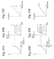
- Figs. 1 and 2 show examples of waveforms of modulated pulses.
- triangular pulses are gradually increased with gradation values increasing from 1 to n
- the pulse widths of trapezoidal pulses are gradually increased with the gradation values increasing from n + 1.
- the black portion of a pulse waveform shows a difference from a pulse waveform located in front of it by one gradation.
- the maximum pulse height value of the modulated pulses is at a V4 level
- Fig. 2 the maximum pulse height value of the modulated pulses is at a V3 level (V4 > V3).
- the modulated pulse of Fig. 1 can express luminance higher than that of the modulated pulse of Fig. 2 .
- Fig. 1 is preferably used, for example, when displaying an image which is preferably displayed with high luminance or when a high luminance display mode is selected.
- control of Fig. 2 is preferably used when displaying an image which is preferably displayed with low luminance or when a low luminance display mode is selected.
- Much lower luminance can be realized by setting the maximum pulse height value to V1 or V2. Further, as described later, it is also preferable to change the maximum pulse height value of each color to correct a difference between light emission efficiencies of fluorescents.
- Fig. 3 shows another example of the waveform of the modulated pulse.
- Symbols a, b, c, d show an integer and have the relation of 1 ⁇ a ⁇ b ⁇ c ⁇ d.
- Controls for gradation values from 1 to "a" are the same as the controls (1) to (3) explained in the example 3 of the modulated pulse.
- a control for superimposing a triangular or trapezoidal pulse (maximum pulse height value: V2) on a trapezoidal pulse (maximum pulse height value: V1) for gradation value "a" is executed.
- a waveform having gradation values a + 1 to a + 3 the waveform is caused to rise up to Vx (V1 ⁇ Vx ⁇ V2) with the first waveform, to fall from Vx to V1 with the third waveform, to hold at V1 with the second waveform, and then to fall from V1 to V0 with the third waveform.
- a waveform having a gradation value of a + 4 the waveform is caused to rise up to V2 with the first waveform, to hold at V2 with the second waveform, to fall from V2 to V1 with the third waveform, to hold at V1 with the second waveform, and then to fall from V1 to V0 with the third waveform.
- the second waveform is controlled to different pulse height values (V1, V2). Controls for gradation values from b + 1 to c, and from c + 1 to d are executed in the same manner.
- the gradation property of the image display apparatus can be more enhanced by the above waveform controls.
- Fig. 4 is a block diagram showing the constitution of an image display apparatus according to the first embodiment of the present invention.
- the image display apparatus has a multi-electron source A1 as a display panel (image display unit) and a drive unit for driving the multi-electron source A1.
- the drive unit is composed of an output data circuit, a modulation circuit A2, a scan circuit A3, a modulation power supply circuit A7, and a scan power supply circuit A8.
- the output data circuit has a timing generation circuit A4, a data conversion circuit A5, a parallel/serial conversion circuit A6, and the like.
- the multi-electron source A1 has a plurality of electron-emitting devices, a plurality of row wires, and a plurality of column wires, and the electron-emitting devices are formed to the intersection portions of the row wires and the column wires.
- a selection electric potential is supplied to the row wires and a modulated pulse is supplied to the column wires
- a drive voltage as a potential difference between the selection electric potential and the modulated pulse is applied to the electron-emitting devices. It is possible for desired electron-emitting device to emit light with desired luminance by appropriately controlling the period of time during which the drive voltage is applied and the value of the drive voltage.
- the modulation circuit A2 is connected to the column wires of the multi-electron source A1.
- the modulation circuit A2 is a circuit for generating a modulation signal (modulated pulse) based on the image data supplied from the output data circuit and outputting the modulation signal to the respective column wires of the multi-electron source A1.
- the modulation power supply circuit A7 is a power supply circuit configured such that it can output several voltage values.
- the modulation power supply circuit A7 not only supplies power to the modulation circuit A2 but also defines the voltage value of the modulated pulse output from the modulation circuit A2.
- the modulation power supply circuit A7 is usually a voltage source circuit, it is not necessarily limited thereto.
- the scan circuit A3 is connected to the row wires of the multi-electron source A1.
- the scan circuit A3 is a circuit for selecting one or several of row wires to be driven among all the row wires and sequentially switching the row wires to be selected.
- the scan circuit A3 adopts line-sequential scanning in which the row wires are selected sequentially one by one, it is not limited thereto.
- the scan circuit A3 may adopt an interlaced scanning, or a scanning in which several adjacent rows are selected at a time (multi line scanning).
- the scan circuit A3 supplies the selection electric potential to a row wire (selected line) to be driven and supplies a non-selection electric potential to the other row wires (non-selected lines).
- the scan power supply circuit A8 is a power supply circuit for outputting several voltage values (selection electric potential, non-selection electric potential). Although the scan power supply circuit A8 is usually a voltage source circuit, it is not necessarily limited thereto.
- the timing generation circuit A4 is a circuit for generating a timing signal as control data for controlling the timings of the modulation circuit A2, the scan circuit A3 , the data conversion circuit A5, and the parallel/serial conversion circuit A6.
- the data conversion circuit A5 is a circuit for converting input luminance gradation data to image data suitable for the modulation circuit A2 and the multi-electron source A1.
- the data conversion circuit A5 can perform various signal processing to the luminance gradation data, such as inverted ⁇ conversion, luminance correction, color correction, resolution conversion, maximum value adjustment (limiter), and the like.
- the parallel/serial conversion circuit A6 is a circuit for converting the image data output from the data conversion circuit 5 from parallel data to serial data and outputting the serial data to the modulation circuit A2.
- Fig. 5 is a block diagram showing the circuit configuration of the modulation circuit A2.
- the modulation circuit A2 is composed of a serial/parallel conversion circuit A9, a shift register A10, a data sampling circuit A11, a logic circuit A12, and an output circuit A13.
- the image data output from the output data circuit is converted into the parallel data in the serial/parallel conversion circuit A9.
- the image data converted into the parallel data is sequentially stored to the data sampling circuit A11 via the shift register A10.
- Image data corresponding to the number of pixels (hereinafter, the number of pixels in the horizontal direction is shown by M) in a horizontal direction of the multi-electron source A1 is stored to the data sampling circuit A11. Thereafter, the logic circuit A12 generates a control signal (control sequence) of the output circuit A13 based on the image data for the respective pixels stored to the data sampling circuit A11 and sends the control signal to the output circuit A13.
- M the number of pixels in the horizontal direction
- the logic circuit A12 generates a control signal (control sequence) of the output circuit A13 based on the image data for the respective pixels stored to the data sampling circuit A11 and sends the control signal to the output circuit A13.
- the output circuit A13 generates a modulated pulse based on the control signal (control sequence) and outputs the modulated pulse to the column wires of the multi-electron source A1.
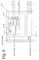
- Fig. 6 is a block diagram showing the constitution of the logic circuit A12 of the modulation circuit.
- the logic circuit A12 has M pieces of logic circuits A14. Each of the logic circuits A14 corresponds to each pixel. A specific constitution and operation of a logic circuit A14 for one pixel will be explained as an example.
- the logic circuit A14 has a decoder A14a and a sequence generation circuit A14b.
- the image data sampled by the data sampling circuit A11 is input to the decoder A14a.
- the decoder A14a From the image data and the timing signal which is output from the output data circuit, the decoder A14a generates control data for timings at which the modulated pulse rises and falls.
- the control data is input to the sequence generation circuit A14b and used as data for a comparator. Further, from the image data and the timing signal, the decoder A14a generates a control signal Level for defining the output level of the modulated pulse.
- the control signal Level is input to the output circuit A13.
- the sequence generation circuit A14b counts the number of clocks based on a clock signal supplied as the timing signal.
- the comparator in the sequence generation circuit A14b compares the value counted by the sequence generation circuit A14b with control data for rising/falling timings. Then, a control signal Tr for defining timing at which the modulated pulse rises and a control signal Tf for defining timing at which the modulated pulse falls are generated based on the value of the comparator.
- the control signals Tr and Tf are input to the output circuit A13.
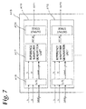
- Fig. 7 is a block diagram showing the constitution of the output circuit A13 of the modulation circuit.
- the output circuit A13 has M pieces of output circuits A15. Each of the output circuits A15 corresponds to each pixel (each column wire). A specific constitution and operation of an output circuit A15 for one pixel will be explained as an example.
- the output circuit A15 is composed of a level shift circuit A16, a reference waveform generation circuit A17, and an output stage A18.
- the control signals Tr and Tf, Level sent from the logic circuit A14 are input to the output circuit A15.
- the level shift circuit A16 converts the voltages of the control signals Tr, Tf and Level from logic level into operation voltage level of the output circuit A15.
- the control signals Tr, Tf and Level output from the level shift circuit A16 are input to the reference waveform generation circuit A17.
- Fig. 8 is a block diagram showing the constitution of the reference waveform generation circuit A17.
- the reference waveform generation circuit A17 is composed of a rising reference waveform generation unit A17a, an output level generation unit A17b, a falling reference waveform generation unit A17c, and a waveform switching unit A17d.
- the rising reference waveform generation unit A17a, the output level generation unit A17b, and the falling reference waveform generation unit A17c correspond to the first waveform generation unit, the second waveform generation unit, and the third waveform generation unit of the present invention, respectively.
- the wave form switching unit A17d corresponds to the waveform switching unit of the present invention.
- the control signal Tr whose level is shifted is input to the rising reference waveform generation unit A17a.
- the rising reference waveform generation unit A17a On receiving the control signal Tr, the rising reference waveform generation unit A17a generates an up-slope waveform having a predetermined inclination and outputs it.
- the up-slope waveform (first waveform) may have any waveform as long as it is a waveform gently rising in a slope shape.
- the up-slope waveform is preferably a monotonically increasing waveform and more preferably a waveform having a constant inclination. This is because such waveform eases gradation control.
- Fig. 9 shows an example of the constitution of a circuit for generating an up-slope waveform.
- the circuit is composed of switches S1, S2, a current source Itr, and a capacitor Ctr.
- the control signal Level whose level is shifted is input to the output level creation unit A17b.
- the output level creation unit A17b performs digital/analog conversion on the control signal Level and outputs a voltage level signal LEVEL_OUT having a constant voltage.
- the voltage level signal LEVEL_OUT has a waveform (second waveform) for defining the maximum pulse height value of the modulated pulse.
- the control signal Tf whose level is shifted is input to the falling reference waveform generation unit A17c.
- the falling reference waveform generation unit A17c receives the voltage of a reference waveform REF_WF output from the waveform switching unit A17d at all times.
- the reason why the falling reference waveform generation unit A17c receives the voltage of the reference waveform REF_WF at all times resides in that it generates a falling waveform from the voltage level output from the waveform switching unit A17d. More specifically, when the control signal Tf is input, the falling reference waveform generation unit A17c generates a down-slope waveform having a predetermined inclination from the voltage value of the reference waveform REF_WF and outputs an output voltage Tf_OUT.
- the down-slope waveform (third waveform) may have any waveform as long as it is a waveform gently falling in a slope shape.
- the down-slope waveform is preferably a monotonically decreasing waveform and more preferably a waveform having a constant inclination. This is because such waveform eases gradation control.
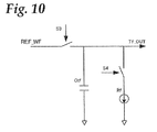
- Fig. 10 shows an example of the constitution of a circuit for generating the down-slope waveform.
- the circuit is composed of switches S3, S4, a current source Itf, and a capacitor Ctf.
- the waveform switching unit A17d generates the reference waveform REF_WF by switching the reference waveform (output voltage) of the rising reference waveform generation unit A17a, the output level generation unit A17b, and the falling reference waveform generation unit A17c based on the control signals Tr, Tf and outputs the reference waveform REF_WF to the output stage A18.
- the waveform switching unit A17d selects the output voltage Tr_OUT of the rising reference waveform generation unit A17a, whereas when the control signal Tr is Low, the waveform switching unit A17d selects the output voltage LEVEL_OUT of the output level generation unit A17b.
- the waveform switching unit A17d operates according to the logic for the control signal Tr, whereas when the control signal Tf is Low, the waveform switching unit A17d selects the output voltage Tf_OUT of the falling reference waveform generation unit A17c.
- the output stage A18 refers to the output waveform REF_WF from the waveform switching unit A17d and generates a modulated pulse having the same waveform or a similar waveform.
- the modulated pulse OUT is output to the column wires of the multi-electron source A1.
- the output stage A18 is preferably configured as a unity gain buffer using an operation amplifier A18a as shown in Fig. 8 . Further, the output stage A18 may employ a constitution of an amplifier stage of the operation amplifier.
- Fig. 11 is a timing chart showing an operation example 1 of the output circuit A15
- Fig. 12 is a logic table of the operation example 1.
- the operation example 1 is a control when a modulated pulse having a maximum voltage level (V4) is output.
- the control signal Level is input to the output level generation unit A17b, and the voltage level signal LEVEL_OUT is output. In the example, level V4 is output.
- the rising reference waveform generation unit A17a When the control signal Tr is at High level, the rising reference waveform generation unit A17a outputs a rising waveform Tr_OUT having a constant inclination. When the control signal Tr is at Low level, Tr_OUT is set to 0 V (ground level).
- the falling reference waveform generation unit A17c takes in a voltage of REF_WF.
- the falling reference waveform generation unit A17c keeps taking in the voltage of REF_WF until the control signal Tf is set to Low level and then outputs the voltage REF_WF as Tf_OUT.
- Tf_OUT falls from REF_WF in a constant inclination and is set to 0 V eventually.
- the waveform switching unit A17d selects and outputs a reference waveform Tr_OUT output from the rising reference waveform generation unit A17a.
- the control signal Tr is kept High during a period in which a voltage of Tr_OUT reaches the V4 level.
- the waveform switching unit A17d selects and outputs LEVEL_OUT, in case that the control signal Tf is at High level. In case that the control signal Tf is at Low level, the waveform switching unit A17d selects and outputs Tf_OUT.
- the reference waveform REF_WF for an output waveform rises from the ground level with a constant inclination, outputs a designated voltage level, and then falls to the ground level with a constant inclination.
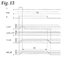
- Fig. 13 is a timing chart showing an operation example 2 of the output circuit A15
- Fig. 14 is a logic table of the operation example 2.
- the operation example 2 shows a control when a modulated pulse having an output level (V3) lower than that of the operation example 1 is output.
- the operation example 2 is different from the operation example 1 in that the voltage of the control signal Level is level V3 and that the High period of the control signal Tr is made short.
- the High period of the control signal Tr is determined depending on a period of time necessary to cause the reference waveform to rise up to the output voltage level V3. As described above, a smooth waveform can be generated by controlling the High period of the control signal Tr according to the output voltage level.
- a period PW in which the output voltage level is output can be controlled by adjusting the High period of the control signals Tr and Tf. With this operation, the pulse width of the reference waveform REF_WF can be controlled.
- output waveforms having other output voltage levels V1 and V2 can be generated likewise.
- Both the operation examples 1, 2 described above execute the pulse width modulations, but the maximum pulse height value of the pulse are different each other.
- the pulse width modulations having the different maximum pulse height value can be preferably used to, for example, color adjustment, adjustment of gradation control characteristics for each color, and the like.
- the image display apparatus of the embodiment realizes RGB emission by collision of the electrons emitted from the multi-electron source against a surface on which RGB phosphors are coated.
- phosphors ordinarily have different light emitting efficiencies in the respective RGB colors. Accordingly, even if the same amounts of electrons (charge amount) are discharged to the phosphors of the respective colors, resultant amounts of emission are not the same.
- RGB can be emitted in the same amount by individually setting drive voltage values to each of RGB in consideration of the light emitting efficiencies and executing the pulse width modulation in the voltage levels.
- Fig. 15A shows the characteristics of the drive voltage Vf vs. emission current Ie of electron-emitting devices formed on the multi-electron source.
- Fig. 15B shows a drive waveform applied to the electron-emitting devices of the respective RGB colors.
- the same drive voltage Vd is applied to the respective RGB colors.
- Fig. 15C shows the luminance characteristics of the respective RGB colors to image data.
- the phosphors have the emission efficiencies of R > G > B. If all the devices for RGB colors are driven by the same drive voltage, it can be found that luminance is different as shown by R > G > B even if the same image data is used.
- the drive voltages of the respective colors are set such that an electron-emitting device corresponding to a phosphor having a higher light emitting efficiency is driven by a lower drive voltage as shown in Fig. 15D .
- a drive voltage Vr for R is set lower than Vd
- a drive voltage Vg for G is set to the same as Vd
- a drive voltage Vb for B is set higher than Vd.
- pulse width modulations having different maximum pulse height values (output voltage levels) are executed for the respective RGB colors as shown in Fig. 15E .
- the luminance characteristics of the respective RGB colors can be caused to coincide with each other as shown in Fig. 15F .
- the gradation characteristics of the respective RGB colors can be adjusted by appropriately selecting the drive voltage values of the respective RGB colors as described above. Note that when a non-linear gradation control such as adjustment of ⁇ characteristics and the like are executed, the non-linear gradation control can be executed by appropriately selecting image data.
- Fig. 16 is a timing chart showing an operation example 3 of the output circuit A15
- Fig. 17 is a logic table of the operation example 3.
- the operation example 3 is different from the operation examples 1 and 2 in that the operation example 3 does not output the voltage level signal LEVEL_OUT having a constant voltage and a rising waveform is instantly switched to a falling waveform. That is, although the modulated pulses of the operation examples 1 and 2 have the trapezoidal waveform, a modulated pulse of the operation example 3 has a triangular waveform.
- the triangular waveform is preferably used to drive, for example, a low gradation.
- Fig. 16 shows an example for generating a triangular waveform from 0 V to a V1 level.
- a triangular reference waveform REF_WF is generated by that both control signals Tr and Tf are switched from High level to Low level at the same timing.
- the size of triangular waveform can be increased by increasing High period of the control signals Tr and Tf.
- the length of High period is set to (a) ⁇ (b) ⁇ (c) ⁇ (d), and the pulse height value of the triangular waveform reaches the V1 level in case of (d).
- Fig. 16 explains the example of the triangular waveform between the 0 V and the V1 level, the triangular waveform can be also output between other voltage levels by appropriately setting the control signals Tr and Tf.
- each of the output circuits A15 has the rising reference waveform generation unit A17a, the output level generation unit A17b, and the falling reference waveform generation unit A17c. Accordingly, each of the output circuits A15 for M pixels can independently control timing at which a modulated pulse rises, a voltage level and an output period thereof, and timing at which the modulated pulse falls. In other words, the modulated pulse can be caused to rise and fall at different timing and the voltage level can be made different for each pixel (each column wire).
- Fig. 18 is a block diagram showing the constitution of a reference waveform generation circuit A17 according to a second embodiment of the present invention.
- the second embodiment is different from the first embodiment in that a plurality of the reference waveform generation circuits A17 shares a common rising reference waveform generation unit A17a and that the second embodiment has a control signal LEVEL_cont for defining timing at which a voltage level signal LEVEL_OUT is output. That is, although the second embodiment has an output level generation unit A17b, a falling reference waveform generation unit A17c, and a waveform switching unit A17d disposed to each of column wires, the number of the rising reference waveform generation units A17a is smaller than that of the column wires.
- a modulation circuit A2 is composed of one or a more integrated circuits (IC chips), and several output circuits A15 are disposed in one integrated circuit.
- the chip size can be reduced by employing such an configuration that all the output circuits A15 in the integrated circuit commonly use the one rising reference waveform generation unit A17a.
- the configuration of the second embodiment can be applied to a control in which a start timing and operational timing of the rising waveform are always same.
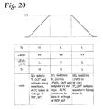
- Fig. 19 is a timing chart showing an operation example 4 of the output circuit A15
- Fig. 20 is a logic table of the operation example 4.
- a control signal Level is input to the output level generation unit A17b, and a voltage level signal LEVEL_OUT is output.
- level V4 is output in the example, the same operation is executed in a level other than the V4 level.
- the control signal LEVEL_cont is a signal for defining timing at which the voltage of the voltage level signal LEVEL_OUT is output.
- the control signal LEVEL_cont can select the signal LEVEL_OUT by setting the control signal Tr of each output circuit to Low.
- a control signal such as the signal LEVEL_OUT is necessary.
- the rising reference waveform generation unit A17a When the control signal Tr is at High level, the rising reference waveform generation unit A17a outputs a rising waveform Tr_OUT having a constant inclination. When the control signal Tr is at Low level, the rising waveform Tr_OUT is set to 0 V (ground level).
- the falling reference waveform generation unit A17c takes in a voltage of REF_WF.
- the falling reference waveform generation unit A17c keeps taking in the voltage of REF_WF until the control signal Tf is set to Low level and then outputs the voltage as Tf_OUT.
- Tf_OUT falls from REF_WF in a constant inclination and eventually becomes 0 V.
- the control signal Level is input to the output level generation unit A17b, and the voltage level signal LEVEL_OUT having a constant level is output.
- the control signal LEVEL_cont is input to the waveform switching unit A17d.
- the waveform switching unit A17d selects LEVEL_OUT, and when the control signal LEVEL_cont is Low, the waveform switching unit A17d operates according to other logic.
- the waveform switching unit A17d selects the reference waveform Tr_OUT output from the rising reference waveform generation unit A17a and outputs the rising reference waveform.
- the control signal LEVEL_cont is set to High level
- the waveform switching unit A17d selects LEVEL_OUT and outputs a level voltage (here, V4).
- the control signal LEVEL_cont is set to Low level and the control signal Tf is set to High level
- the waveform switching unit A17d selects Tf_OUT and outputs a falling waveform.
- control signal Tr is used as a timing signal of several output circuits, it is set to High level while at least one output circuit rises and set to Low level after the rising of all the output circuits is completed.
- each of the output circuits A15 has the output level generation unit A17b and the falling reference waveform generation unit A17c. Accordingly, each of the output circuits A15 for M pixels can independently control a voltage level, an output period thereof, and timing at which the voltage level falls. In other words, the modulated pulse can be caused to fall at different timing and the voltage level can be made different for each pixel (each column wire).
- LEVEL_OUT is set to a constant voltage level in the operation examples 1 to 4 described above, the voltage level of LEVEL_OUT can be also changed by changing the designating value of the control signal Level in one horizontal period (1H).
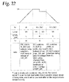
- Fig. 21 is a timing chart showing an operation example 5 of the output circuit A15
- Fig. 22 is a logic table of the operation example 5.
- LEVEL_OUT is set to the V4 level at all times during the period in which the control signal Level is at High level in the operation example 4, LEVEL_OUT is switched from the V4 level to the V3 level at certain timing in the operation example 5. With this operation, the output level can be changed in the one horizontal period (1H).
- the output level can be arbitrarily changed by controlling the control signal Level.
- the output level can be also changed at two or more stages in the one horizontal period (1H).
- the operation example 5 is realized by the circuit configuration of the second embodiment here, a similar modulated pulse waveform can be also generated using the circuit configuration of the first embodiment.
- the output stage A18 of the above embodiments employs a configuration for outputting a reference waveform by an amplifier or a buffer.
- a configuration for outputting a reference waveform by an amplifier or a buffer When an output having the same level as that of a power supply voltage is necessary here, it is preferable to provide switches SH and SL for outputting power supply voltages as shown in Fig. 23 . With this configuration, outputs having the same levels as those of power supply voltages VCC and VSS can be stably obtained.
- a power supply voltage VCC can be directly output in such a manner that the rising portion thereof is raised by the operation amplifier A18a and thereafter the switch SH is turned on.
- a power supply voltage (reference voltage) VSS can be directly output in such a manner that the switch SH is turned off, the voltage is completely dropped by the operation amplifier A18a, and thereafter the switch SL turned on.
- a modulation circuit has a first waveform generation unit for generating a first waveform which rises in a slope shape, a second waveform generation unit for generating a second waveform which defining a pulse height value, a third waveform generation unit for generating a third waveform which falls in a slope shape, and a waveform switching unit.
- the waveform switching unit generates a waveform of a modulated pulse by combining the first waveform and the third waveform or the first waveform, the second waveform, and the third waveform according to a control signal generated by image data. This constitution suppresses disturbance of a modulated pulse waveform at a voltage transition.
Landscapes
- Engineering & Computer Science (AREA)
- Physics & Mathematics (AREA)
- Computer Hardware Design (AREA)
- General Physics & Mathematics (AREA)
- Theoretical Computer Science (AREA)
- Control Of Indicators Other Than Cathode Ray Tubes (AREA)
- Details Of Television Scanning (AREA)
Applications Claiming Priority (1)
| Application Number | Priority Date | Filing Date | Title |
|---|---|---|---|
| JP2008095453A JP2009251046A (ja) | 2008-04-01 | 2008-04-01 | 画像表示装置およびその制御方法 |
Publications (2)
| Publication Number | Publication Date |
|---|---|
| EP2107547A2 true EP2107547A2 (de) | 2009-10-07 |
| EP2107547A3 EP2107547A3 (de) | 2010-05-05 |
Family
ID=40718571
Family Applications (1)
| Application Number | Title | Priority Date | Filing Date |
|---|---|---|---|
| EP09156876A Withdrawn EP2107547A3 (de) | 2008-04-01 | 2009-03-31 | Bildanzeigevorrichtung und Steuerverfahren dafür |
Country Status (4)
| Country | Link |
|---|---|
| US (1) | US8259140B2 (de) |
| EP (1) | EP2107547A3 (de) |
| JP (1) | JP2009251046A (de) |
| CN (1) | CN101551967A (de) |
Families Citing this family (5)
| Publication number | Priority date | Publication date | Assignee | Title |
|---|---|---|---|---|
| TWI336461B (en) * | 2007-03-15 | 2011-01-21 | Au Optronics Corp | Liquid crystal display and pulse adjustment circuit thereof |
| JP2009251046A (ja) * | 2008-04-01 | 2009-10-29 | Canon Inc | 画像表示装置およびその制御方法 |
| CN109754758B (zh) | 2017-11-01 | 2020-11-03 | 元太科技工业股份有限公司 | 显示面板的驱动方法 |
| KR102532203B1 (ko) | 2018-07-31 | 2023-05-12 | 삼성전자 주식회사 | 전압 생성기, 전압 파형 생성기, 반도체 소자 제조 장치, 전압 파형 발생 방법 및 반도체 소자의 제조 방법 |
| CN119889233A (zh) * | 2025-03-28 | 2025-04-25 | 国鲸合创(青岛)科技有限公司 | 高分辨率有机显示驱动波形生成方法 |
Citations (3)
| Publication number | Priority date | Publication date | Assignee | Title |
|---|---|---|---|---|
| JP2003173159A (ja) | 2001-06-15 | 2003-06-20 | Canon Inc | 駆動回路及び表示装置及び駆動方法 |
| US20060066523A1 (en) * | 2004-09-30 | 2006-03-30 | Kabushiki Kaisha Toshiba | Display device and display method |
| EP1650732A2 (de) | 2004-10-14 | 2006-04-26 | Ngk Insulators, Ltd. | Elektronen-emittierende Vorrichtung |
Family Cites Families (12)
| Publication number | Priority date | Publication date | Assignee | Title |
|---|---|---|---|---|
| US5687067A (en) * | 1995-05-30 | 1997-11-11 | Philips Electronics North America Corporation | Low noise controller for pulse width modulated converters |
| GB9704149D0 (en) * | 1996-08-16 | 1997-04-16 | Philips Electronics Nv | Active matrix display devices and methods of driving such |
| JP3630290B2 (ja) * | 1998-09-28 | 2005-03-16 | パイオニアプラズマディスプレイ株式会社 | プラズマディスプレイパネルの駆動方法およびプラズマディスプレイ |
| JP4538915B2 (ja) * | 2000-07-24 | 2010-09-08 | セイコーエプソン株式会社 | 電気光学装置の駆動方法 |
| JP5063841B2 (ja) * | 2001-06-27 | 2012-10-31 | パナソニック株式会社 | プラズマディスプレイパネルの駆動方法 |
| JP2004302025A (ja) | 2003-03-31 | 2004-10-28 | Tohoku Pioneer Corp | 発光表示パネルの駆動方法および駆動装置 |
| EP1605432B1 (de) | 2004-06-01 | 2010-10-06 | LG Display Co., Ltd. | Organische Elektrolumineszenzanzeige und Ansteuerverfahren dafür |
| CN101944346A (zh) * | 2005-11-04 | 2011-01-12 | 夏普株式会社 | 显示装置 |
| KR100788577B1 (ko) * | 2006-12-27 | 2007-12-26 | 삼성에스디아이 주식회사 | 플라즈마 표시 장치 및 그의 구동 방법 |
| WO2008132854A1 (ja) * | 2007-04-25 | 2008-11-06 | Panasonic Corporation | プラズマディスプレイパネルの駆動方法およびプラズマディスプレイ装置 |
| JP2009251046A (ja) * | 2008-04-01 | 2009-10-29 | Canon Inc | 画像表示装置およびその制御方法 |
| JP5458540B2 (ja) * | 2008-09-29 | 2014-04-02 | セイコーエプソン株式会社 | 画素回路の駆動方法、発光装置および電子機器 |
-
2008
- 2008-04-01 JP JP2008095453A patent/JP2009251046A/ja not_active Withdrawn
-
2009
- 2009-03-27 US US12/412,941 patent/US8259140B2/en not_active Expired - Fee Related
- 2009-03-31 EP EP09156876A patent/EP2107547A3/de not_active Withdrawn
- 2009-04-01 CN CNA2009101298981A patent/CN101551967A/zh active Pending
Patent Citations (3)
| Publication number | Priority date | Publication date | Assignee | Title |
|---|---|---|---|---|
| JP2003173159A (ja) | 2001-06-15 | 2003-06-20 | Canon Inc | 駆動回路及び表示装置及び駆動方法 |
| US20060066523A1 (en) * | 2004-09-30 | 2006-03-30 | Kabushiki Kaisha Toshiba | Display device and display method |
| EP1650732A2 (de) | 2004-10-14 | 2006-04-26 | Ngk Insulators, Ltd. | Elektronen-emittierende Vorrichtung |
Also Published As
| Publication number | Publication date |
|---|---|
| US8259140B2 (en) | 2012-09-04 |
| JP2009251046A (ja) | 2009-10-29 |
| EP2107547A3 (de) | 2010-05-05 |
| US20090244038A1 (en) | 2009-10-01 |
| CN101551967A (zh) | 2009-10-07 |
Similar Documents
| Publication | Publication Date | Title |
|---|---|---|
| US7358935B2 (en) | Display device of digital drive type | |
| US7038394B2 (en) | Ramp voltage generating apparatus and active matrix drive-type display apparatus | |
| KR20240056462A (ko) | 감마 전압 생성 회로, 이를 포함하는 소스 드라이버 및 표시 장치 | |
| US20070211011A1 (en) | Flat panel display device and data signal generating method thereof | |
| US7679628B2 (en) | Controller and image display device | |
| KR102657981B1 (ko) | 감마 전압 생성 회로, 이를 포함하는 소스 드라이버 및 표시 장치 | |
| US8259140B2 (en) | Method of controlling an image display apparatus | |
| CN118355426A (zh) | 显示面板的驱动电路 | |
| US7277105B2 (en) | Drive control apparatus and method for matrix panel | |
| US20100309232A1 (en) | Control method for image display apparatus | |
| US7474168B2 (en) | Modulation-signal generator circuit, image display apparatus and television apparatus | |
| CN116940977A (zh) | 驱动控制装置、驱动控制方法及信息处理系统 | |
| US20060071881A1 (en) | Line-at-a-time addressed display and drive method | |
| CN100530289C (zh) | 具有减小信号失真的电子发射显示器(eed)及驱动eed的方法 | |
| KR100801782B1 (ko) | 주사회로, 주사장치, 화상표시장치 및 텔레비전장치 | |
| JP2009258223A (ja) | 画像表示装置 | |
| EP2088573A2 (de) | Ansteuerungsschaltung für Anzeigefeld und Anzeigevorrichtung | |
| JP4453136B2 (ja) | マトリクス型画像表示装置 | |
| JP2005208259A (ja) | 有機elディスプレイ装置の駆動装置および駆動方法 | |
| JP2009211053A (ja) | 表示パネルの駆動回路および表示装置 | |
| CN100587770C (zh) | 扫描电路、扫描装置、图像显示装置和电视装置 | |
| JP2007232902A (ja) | 有機elディスプレイ装置の駆動装置 | |
| JP2006084818A (ja) | 発光表示装置の駆動装置 | |
| JP2004117910A (ja) | 有機elディスプレイ装置の駆動方法 | |
| KR20060012159A (ko) | 전자방출원 안정화 수단을 구비한 전자 방출 장치 |
Legal Events
| Date | Code | Title | Description |
|---|---|---|---|
| PUAI | Public reference made under article 153(3) epc to a published international application that has entered the european phase |
Free format text: ORIGINAL CODE: 0009012 |
|
| AK | Designated contracting states |
Kind code of ref document: A2 Designated state(s): AT BE BG CH CY CZ DE DK EE ES FI FR GB GR HR HU IE IS IT LI LT LU LV MC MK MT NL NO PL PT RO SE SI SK TR |
|
| AX | Request for extension of the european patent |
Extension state: AL BA RS |
|
| PUAL | Search report despatched |
Free format text: ORIGINAL CODE: 0009013 |
|
| AK | Designated contracting states |
Kind code of ref document: A3 Designated state(s): AT BE BG CH CY CZ DE DK EE ES FI FR GB GR HR HU IE IS IT LI LT LU LV MC MK MT NL NO PL PT RO SE SI SK TR |
|
| AX | Request for extension of the european patent |
Extension state: AL BA RS |
|
| RIC1 | Information provided on ipc code assigned before grant |
Ipc: G09G 3/20 20060101ALI20100329BHEP Ipc: H03K 17/16 20060101ALI20100329BHEP Ipc: H03K 5/12 20060101ALI20100329BHEP Ipc: G09G 3/22 20060101AFI20090617BHEP |
|
| 17P | Request for examination filed |
Effective date: 20101105 |
|
| AKX | Designation fees paid |
Designated state(s): DE FR GB |
|
| 17Q | First examination report despatched |
Effective date: 20110110 |
|
| STAA | Information on the status of an ep patent application or granted ep patent |
Free format text: STATUS: THE APPLICATION HAS BEEN WITHDRAWN |
|
| 18W | Application withdrawn |
Effective date: 20120530 |