EP2107577A1 - Composant inductif et procédé de sa fabrication - Google Patents
Composant inductif et procédé de sa fabrication Download PDFInfo
- Publication number
- EP2107577A1 EP2107577A1 EP09004651A EP09004651A EP2107577A1 EP 2107577 A1 EP2107577 A1 EP 2107577A1 EP 09004651 A EP09004651 A EP 09004651A EP 09004651 A EP09004651 A EP 09004651A EP 2107577 A1 EP2107577 A1 EP 2107577A1
- Authority
- EP
- European Patent Office
- Prior art keywords
- circuit board
- coil
- component
- printed circuit
- induction component
- Prior art date
- Legal status (The legal status is an assumption and is not a legal conclusion. Google has not performed a legal analysis and makes no representation as to the accuracy of the status listed.)
- Granted
Links
Images



Classifications
-
- H—ELECTRICITY
- H05—ELECTRIC TECHNIQUES NOT OTHERWISE PROVIDED FOR
- H05K—PRINTED CIRCUITS; CASINGS OR CONSTRUCTIONAL DETAILS OF ELECTRIC APPARATUS; MANUFACTURE OF ASSEMBLAGES OF ELECTRICAL COMPONENTS
- H05K1/00—Printed circuits
- H05K1/18—Printed circuits structurally associated with non-printed electric components
- H05K1/182—Printed circuits structurally associated with non-printed electric components associated with components mounted in printed circuit boards [PCB], e.g. insert-mounted components [IMC]
- H05K1/185—Printed circuits structurally associated with non-printed electric components associated with components mounted in printed circuit boards [PCB], e.g. insert-mounted components [IMC] associated with components encapsulated in the insulating substrate of the PCBs; associated with components incorporated in internal layers of multilayer circuit boards
-
- H—ELECTRICITY
- H01—ELECTRIC ELEMENTS
- H01F—MAGNETS; INDUCTANCES; TRANSFORMERS; SELECTION OF MATERIALS FOR THEIR MAGNETIC PROPERTIES
- H01F17/00—Fixed inductances of the signal type
- H01F17/0006—Printed inductances
-
- H—ELECTRICITY
- H01—ELECTRIC ELEMENTS
- H01F—MAGNETS; INDUCTANCES; TRANSFORMERS; SELECTION OF MATERIALS FOR THEIR MAGNETIC PROPERTIES
- H01F27/00—Details of transformers or inductances, in general
- H01F27/28—Coils; Windings; Conductive connections
- H01F27/2847—Sheets; Strips
-
- H—ELECTRICITY
- H01—ELECTRIC ELEMENTS
- H01F—MAGNETS; INDUCTANCES; TRANSFORMERS; SELECTION OF MATERIALS FOR THEIR MAGNETIC PROPERTIES
- H01F41/00—Apparatus or processes specially adapted for manufacturing or assembling magnets, inductances or transformers; Apparatus or processes specially adapted for manufacturing materials characterised by their magnetic properties
- H01F41/02—Apparatus or processes specially adapted for manufacturing or assembling magnets, inductances or transformers; Apparatus or processes specially adapted for manufacturing materials characterised by their magnetic properties for manufacturing cores, coils, or magnets
- H01F41/04—Apparatus or processes specially adapted for manufacturing or assembling magnets, inductances or transformers; Apparatus or processes specially adapted for manufacturing materials characterised by their magnetic properties for manufacturing cores, coils, or magnets for manufacturing coils
- H01F41/041—Printed circuit coils
-
- H—ELECTRICITY
- H01—ELECTRIC ELEMENTS
- H01F—MAGNETS; INDUCTANCES; TRANSFORMERS; SELECTION OF MATERIALS FOR THEIR MAGNETIC PROPERTIES
- H01F17/00—Fixed inductances of the signal type
- H01F17/04—Fixed inductances of the signal type with magnetic core
-
- H—ELECTRICITY
- H01—ELECTRIC ELEMENTS
- H01F—MAGNETS; INDUCTANCES; TRANSFORMERS; SELECTION OF MATERIALS FOR THEIR MAGNETIC PROPERTIES
- H01F27/00—Details of transformers or inductances, in general
- H01F27/28—Coils; Windings; Conductive connections
- H01F27/2847—Sheets; Strips
- H01F2027/2861—Coil formed by folding a blank
-
- H—ELECTRICITY
- H05—ELECTRIC TECHNIQUES NOT OTHERWISE PROVIDED FOR
- H05K—PRINTED CIRCUITS; CASINGS OR CONSTRUCTIONAL DETAILS OF ELECTRIC APPARATUS; MANUFACTURE OF ASSEMBLAGES OF ELECTRICAL COMPONENTS
- H05K2201/00—Indexing scheme relating to printed circuits covered by H05K1/00
- H05K2201/08—Magnetic details
- H05K2201/083—Magnetic materials
- H05K2201/086—Magnetic materials for inductive purposes, e.g. printed inductor with ferrite core
-
- H—ELECTRICITY
- H05—ELECTRIC TECHNIQUES NOT OTHERWISE PROVIDED FOR
- H05K—PRINTED CIRCUITS; CASINGS OR CONSTRUCTIONAL DETAILS OF ELECTRIC APPARATUS; MANUFACTURE OF ASSEMBLAGES OF ELECTRICAL COMPONENTS
- H05K2201/00—Indexing scheme relating to printed circuits covered by H05K1/00
- H05K2201/10—Details of components or other objects attached to or integrated in a printed circuit board
- H05K2201/10007—Types of components
- H05K2201/1003—Non-printed inductor
-
- H—ELECTRICITY
- H05—ELECTRIC TECHNIQUES NOT OTHERWISE PROVIDED FOR
- H05K—PRINTED CIRCUITS; CASINGS OR CONSTRUCTIONAL DETAILS OF ELECTRIC APPARATUS; MANUFACTURE OF ASSEMBLAGES OF ELECTRICAL COMPONENTS
- H05K3/00—Apparatus or processes for manufacturing printed circuits
- H05K3/46—Manufacturing multilayer circuits
- H05K3/4602—Manufacturing multilayer circuits characterized by a special circuit board as base or central core whereon additional circuit layers are built or additional circuit boards are laminated
-
- H—ELECTRICITY
- H05—ELECTRIC TECHNIQUES NOT OTHERWISE PROVIDED FOR
- H05K—PRINTED CIRCUITS; CASINGS OR CONSTRUCTIONAL DETAILS OF ELECTRIC APPARATUS; MANUFACTURE OF ASSEMBLAGES OF ELECTRICAL COMPONENTS
- H05K3/00—Apparatus or processes for manufacturing printed circuits
- H05K3/46—Manufacturing multilayer circuits
- H05K3/4644—Manufacturing multilayer circuits by building the multilayer layer by layer, i.e. build-up multilayer circuits
- H05K3/4652—Adding a circuit layer by laminating a metal foil or a preformed metal foil pattern
Definitions
- the invention relates to an induction component with at least one, preferably a plurality of coils.
- induction components are needed in electronics. They are used in connection with circuit boards, with their tracks they must be electrically connected.
- An induction component is already known ( US 6662431 ).
- This induction component has a housing which is box-shaped and has an open underside facing the printed circuit board.
- the front ends of the housing are higher than the side walls, so that the front ends can rest on the circuit board during assembly of the component.
- the connection elements of the housing are formed in the side walls, wherein a leg protrudes from the edges of the side walls.
- the ends of the coil turns are wound around the protruding leg. In this way, a connection of the coil turns with the connection elements of the housing.
- the connection elements of the housing serve to connect the coils with the tracks of the circuit board.
- the invention is based on the object to provide an induction component with at least one coil, which can be produced with little effort and few possibilities for error and is particularly well suited for connection to printed conductors of printed circuit boards.
- the invention proposes an induction component with the features mentioned in claim 1.
- the invention also proposes a method for producing such a component. Further developments of the invention are the subject of the respective dependent claims.
- This proposed by the invention induction component thus contains the at least one coil in a cavity of the circuit board or a piece of printed circuit board.
- the component is thus a piece of printed circuit board.
- the at least one coil may be a wound wire coil or a convoluted coil.
- this induction component not only contains one or more coils, but further for certain functions useful, necessary or required electrical, electronic or other components.
- Such an electronic component can for example also be accommodated in the cavity in which the coil is arranged.
- This component can be placed horizontally, ie parallel to the outside of the circuit board, or vertically. This can be done independently of the coil to be used, ie prefabricated. It is also possible that this additional component is arranged on the coil to be used, that is connected to this.
- an additional electronic component is introduced directly into a layer of a multilayer printed circuit board independently of a coil to be inserted.
- the printed circuit board is also a multilayer printed circuit board, in particular if further functions are to be accommodated in the induction component.
- the induction component has a discrete or a printed ferrite core for the coil.
- the induction component may possibly also contain a further electronic component.
- the invention may be provided in a further development to accommodate such a component not only in a cavity of the circuit board, but also on an outer layer of the circuit board.
- the arrangement of a component on an inner layer can either be a discrete component with the component, or even a printing of such a component.
- the combination of several coils by pressing to form a single manageable component of an induction component according to the invention can also be done in such a way that a ferrite core is added to this component, so that once again a single handle can be used Component for insertion into a cavity of the circuit board is formed.
- the ferrite core which may be, for example, a toroidal core, or a U-core or an E-core, may be arranged to protrude from both sides of the coils and also from the assembled circuit board.
- a Faltflex is formed as an electronic component with inductance component and / or capacitance component and / or resistance component.
- the induction component may have an element that can be used as inductance, capacitance and / or resistance alone or in combination with the printing or assembly.
- the method for producing such an induction component is such that a recess is made in the core layer of a piece of printed circuit board. In this recess, the coil or a package of coils is introduced. Subsequently, the recess is closed by laminating a prepreg on both sides and then a metallic cover layer. The electrically conductive connection can then take place in a known manner.
- this metallic cover layer on one side or on both sides can be removed beforehand.
- the removal of the cover layer can, for example, in one operation with the production of the recess take place, which forms a cavity in the circuit board after production.
- a component for attaching a component to an inner layer, for example, even an inner layer of a coil, it can be provided that the further components are mounted on a printed with coil turns foil before their folds, either by Vorbe Divisionung or by imprinting.
- a ferrite core which is to be common to several coils, can be connected, for example, before introducing the coils into the cavity of the printed circuit board with these.
- the starting point for the production of the induction component according to the invention is a conventional printed circuit board with a core layer 1 and two metallic cover layers 2.
- the cover layers 2 are removed so that only the core layer 1 remains.
- a recess 3 is introduced, which passes in the example shown from one side to the other side of the core layer 1.
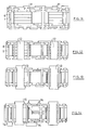
- FIG. 3 two Faltflex coils 4, 5 are shown. It is indicated that these are composed of several layers of folded film with coil turns. These Faltflex coils are known, they can have different sizes, shapes and different values.
- FIG. 5 shows the end result of the just described method, namely an induction component, which is formed as a self-contained piece of a printed circuit board and can now be electrically and mechanically connected in this state, for example, with another circuit board. It is also conceivable and possible that such induction components is part of a larger printed circuit board, in which further functions are included.
- an induction component which is formed as a self-contained piece of a printed circuit board and can now be electrically and mechanically connected in this state, for example, with another circuit board. It is also conceivable and possible that such induction components is part of a larger printed circuit board, in which further functions are included.
- FIG. 6 shows a method step in another manufacturing method, in which after the in FIG. 2 illustrated method step, this time with two cavities 3, first a circuit board layout 10 is applied to the two side surfaces of the core layer. Subsequently, in each case a Faltflex coil 5 are inserted into the two cavities 3. Thereafter, the two side surfaces of the core layer 1 are again laminated with a prepreg layer 6 and a metallic cover layer 7. This creates an intermediate that is in FIG. 8 is shown. So there are two levels of tracks on each side of the core layer. Now, on the outer metallic cover layer 7 again a printed circuit board layout can be formed, so that the in FIG. 9 shown in section arrangement arises. Again, it is an induction component with two Faltflex coils which are electrically connected by transversely through the circuit board passing conductor tracks 8 and the circuit board element on both sides.
- Faltflex coils 4, 5 may also be packages of coils in which a plurality of coils are pressed together so that they appear as a single component and can be used in this way in cavities.
- the induction component the in FIG. 10 is shown, the manufacturing operations are not shown in detail, since they run in principle the same as in the aforementioned embodiments. It In this example, on each side of the original core layer, there are three levels of possible tracks. The connection from the outer level to the middle level is done by micro vias 11.
- FIGS. 9 and 10 While with in the FIGS. 9 and 10
- FIG. 11 an embodiment in which the AnARM mich the coil is not done by passing through them cross-connections, but with the help of printed conductor leads from the flat sides of the coil packages ago, for example by the microvias 11 in the FIG. 11 ,
- FIG. 12 shows a further embodiment in which through recesses 12 are introduced into an already largely manufactured induction component, in which then ferrite cores 13 are used, see FIG. 13 ,
- FIG. 14 shows that on the outer layers of the circuit board additional electronic components 14 can be placed, which are also operatively connected to the induction component.
- further electronic components 15 are contained in intermediate layers within the core layer.
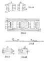
- the ferrite cores 13 are inserted later. In the final result shown, see FIG. 14 , then the ends of the ferrite cores 13 are accessible from the outside of the induction component ago. But it is also possible in the production of compressed Faltflex coils to form a handle as a single element component equal to insert a ferrite core 13, either as a discrete ferrite core or as a printed ferrite core. This is in FIG. 15 schematically shown. Then, such a device 16 can be inserted into the cavity 3 of the core layer 1. Subsequently, a pressing is again carried out with a prepreg layer 6 and a metallic cover layer 7 on both sides. The further treatment then corresponds to what has been described so far.
- FIG. 17 shows a component of pressed together Faltflex coils 4, on whose two peripheral sides 17 each have an electronic component 18 is attached, whose extension thus extends transversely to the surface of the core layer or circuit board.
- FIG. 18 It is also possible to arrange additional electronic components between the layers of a Faltflex coil. This is schematically in FIG. 18 shown.
- Starting point for a Faltflex coil is a film 19 with printed or otherwise arranged coil turns, which are arranged in a specific repeat, so that after folding then the coil turns are superimposed.
- electronic components 18 may be attached, for example, as discrete components, or printed. After folding, see FIG. 19 , These components 18 are then within the Faltflex coil, possibly also at different locations within this coil.
- FIG. 20 now shows an induction component, in which the different options described so far are combined.
- additional electronic components 18 are arranged within the circuit board, which are either connected to a Faltflex coil, or even independently of the Faltflex coil and are mounted independently of a cavity in the intermediate layer, as shown for example in the middle.
Landscapes
- Engineering & Computer Science (AREA)
- Power Engineering (AREA)
- Microelectronics & Electronic Packaging (AREA)
- Manufacturing & Machinery (AREA)
- Coils Or Transformers For Communication (AREA)
Priority Applications (1)
| Application Number | Priority Date | Filing Date | Title |
|---|---|---|---|
| EP09004651.7A EP2107577B1 (fr) | 2008-03-31 | 2009-03-31 | Composant inductif et procédé de sa fabrication |
Applications Claiming Priority (3)
| Application Number | Priority Date | Filing Date | Title |
|---|---|---|---|
| DE200810017303 DE102008017303A1 (de) | 2008-03-31 | 2008-03-31 | Induktionsbauteil |
| EP08162811.7A EP2107576B1 (fr) | 2008-03-31 | 2008-08-22 | Composant à induction |
| EP09004651.7A EP2107577B1 (fr) | 2008-03-31 | 2009-03-31 | Composant inductif et procédé de sa fabrication |
Publications (2)
| Publication Number | Publication Date |
|---|---|
| EP2107577A1 true EP2107577A1 (fr) | 2009-10-07 |
| EP2107577B1 EP2107577B1 (fr) | 2016-10-19 |
Family
ID=40674084
Family Applications (1)
| Application Number | Title | Priority Date | Filing Date |
|---|---|---|---|
| EP09004651.7A Not-in-force EP2107577B1 (fr) | 2008-03-31 | 2009-03-31 | Composant inductif et procédé de sa fabrication |
Country Status (1)
| Country | Link |
|---|---|
| EP (1) | EP2107577B1 (fr) |
Cited By (3)
| Publication number | Priority date | Publication date | Assignee | Title |
|---|---|---|---|---|
| EP3340260A1 (fr) * | 2016-12-22 | 2018-06-27 | AT & S Austria Technologie & Systemtechnik Aktiengesellschaft | Inducteur constitué d'un matériau support de composant comprenant des structures de plaques électroconductrices |
| DE102018114785A1 (de) | 2018-04-13 | 2019-10-17 | Trafag Ag | Verfahren zum Herstellen einer Planarspulenanordnung sowie eines damit versehenen Sensorkopfes |
| EP3605564A1 (fr) * | 2018-07-30 | 2020-02-05 | AT & S Austria Technologie & Systemtechnik Aktiengesellschaft | Support de composant comprenant un inducteur intégré pourvu d'un insert |
Citations (5)
| Publication number | Priority date | Publication date | Assignee | Title |
|---|---|---|---|---|
| WO1998056016A1 (fr) | 1997-06-02 | 1998-12-10 | Vacuumschmelze Gmbh | Composant inductif |
| US6148500A (en) * | 1995-07-24 | 2000-11-21 | Autosplice Systems Inc. | Electronic inductive device and method for manufacturing |
| US20030080845A1 (en) | 2001-10-05 | 2003-05-01 | Fontanella Mark D. | Fabrication approaches for the formation of planar inductors and transformers |
| DE10154833A1 (de) * | 2001-11-08 | 2003-05-22 | Infineon Technologies Ag | Induktor und Verfahren zu seiner Herstellung |
| US6662431B1 (en) | 1997-08-06 | 2003-12-16 | Halo Electronics, Inc. | Electronic surface mount package |
-
2009
- 2009-03-31 EP EP09004651.7A patent/EP2107577B1/fr not_active Not-in-force
Patent Citations (5)
| Publication number | Priority date | Publication date | Assignee | Title |
|---|---|---|---|---|
| US6148500A (en) * | 1995-07-24 | 2000-11-21 | Autosplice Systems Inc. | Electronic inductive device and method for manufacturing |
| WO1998056016A1 (fr) | 1997-06-02 | 1998-12-10 | Vacuumschmelze Gmbh | Composant inductif |
| US6662431B1 (en) | 1997-08-06 | 2003-12-16 | Halo Electronics, Inc. | Electronic surface mount package |
| US20030080845A1 (en) | 2001-10-05 | 2003-05-01 | Fontanella Mark D. | Fabrication approaches for the formation of planar inductors and transformers |
| DE10154833A1 (de) * | 2001-11-08 | 2003-05-22 | Infineon Technologies Ag | Induktor und Verfahren zu seiner Herstellung |
Cited By (12)
| Publication number | Priority date | Publication date | Assignee | Title |
|---|---|---|---|---|
| EP3340260A1 (fr) * | 2016-12-22 | 2018-06-27 | AT & S Austria Technologie & Systemtechnik Aktiengesellschaft | Inducteur constitué d'un matériau support de composant comprenant des structures de plaques électroconductrices |
| CN108231365A (zh) * | 2016-12-22 | 2018-06-29 | 奥特斯奥地利科技与系统技术有限公司 | 包括导电板结构的由器件载体材料制成的电感器 |
| US10861636B2 (en) | 2016-12-22 | 2020-12-08 | At&S Austria Technologie & Systemtechnik Aktiengesellschaft | Inductor made of component carrier material comprising electrically conductive plate structures |
| CN108231365B (zh) * | 2016-12-22 | 2021-05-11 | 奥特斯奥地利科技与系统技术有限公司 | 包括导电板结构的由器件载体材料制成的电感器 |
| EP3944271A1 (fr) * | 2016-12-22 | 2022-01-26 | AT & S Austria Technologie & Systemtechnik Aktiengesellschaft | Inducteur constitué d'un matériau support de composant comprenant des structures de plaques électroconductrices |
| US12002614B2 (en) | 2016-12-22 | 2024-06-04 | At&S Austria Technologie & Systemtechnik Ag | Inductor made of component carrier material comprising electrically conductive plate structures |
| DE102018114785A1 (de) | 2018-04-13 | 2019-10-17 | Trafag Ag | Verfahren zum Herstellen einer Planarspulenanordnung sowie eines damit versehenen Sensorkopfes |
| WO2019197500A1 (fr) | 2018-04-13 | 2019-10-17 | Trafag Ag | Procédé de production d'un ensemble de bobine plane et d'une tête de capteur équipée de celui-ci |
| EP3605564A1 (fr) * | 2018-07-30 | 2020-02-05 | AT & S Austria Technologie & Systemtechnik Aktiengesellschaft | Support de composant comprenant un inducteur intégré pourvu d'un insert |
| CN110797172A (zh) * | 2018-07-30 | 2020-02-14 | 奥特斯奥地利科技与系统技术有限公司 | 包括具有嵌体的嵌入的电感器的部件承载件 |
| US11398334B2 (en) | 2018-07-30 | 2022-07-26 | At&S Austria Technologie & Systemtechnik Aktiengesellschaft | Component carrier comprising embedded inductor with an inlay |
| CN110797172B (zh) * | 2018-07-30 | 2024-05-07 | 奥特斯奥地利科技与系统技术有限公司 | 包括具有嵌体的嵌入的电感器的部件承载件 |
Also Published As
| Publication number | Publication date |
|---|---|
| EP2107577B1 (fr) | 2016-10-19 |
Similar Documents
| Publication | Publication Date | Title |
|---|---|---|
| DE69510630T2 (de) | Leiterrahmen mit einem induktor oder einer ähnlichen magnetischen komponente | |
| DE19508011C2 (de) | Elektromagnetische Ventileinheit | |
| EP0473875A1 (fr) | Procédé pour la fabrication d'un dispostif avec bobine magnétique HF à construction de type puce | |
| WO2014139674A1 (fr) | Composant électronique et procédé de fabrication d'un composant électronique | |
| DE102012003364A1 (de) | Planarer Übertrager | |
| DE102016203613A1 (de) | Elektronisches Bauelement und Verfahren zu dessen Herstellung | |
| WO2016193017A1 (fr) | Transformateur plan pour le transfert d'énergie | |
| DE10245688A1 (de) | Mehrschichtkeramikelektronikteil, Elektronikteilaggregat und Verfahren zum Herstellen eines Mehrschichtkeramikelektronikteils | |
| DE4337053A1 (de) | Spule | |
| EP2107577B1 (fr) | Composant inductif et procédé de sa fabrication | |
| WO2013057266A1 (fr) | Transformateur haute tension et corps de bobine enroulé pour module d'allumage pourvu de tiges de raccordement comme partie constitutive de l'enroulement primaire | |
| DE102009010874A1 (de) | Mehrlagige Schaltungsanordnung und Verfahren zu deren Herstellung | |
| EP2107576B1 (fr) | Composant à induction | |
| DE3722124A1 (de) | Flachbaugruppe mit einer spule oder einem uebertrager | |
| DE102010014281A1 (de) | Induktive elektronische Baugruppe und Verwendung einer solchen | |
| EP1971193A1 (fr) | Composant de plaque conductrice destiné à la fabrication d'inductances planaires à formage de noyau fermé | |
| WO2008128912A1 (fr) | Composant électronique | |
| WO2016155969A2 (fr) | Composant inductif et procédé de réalisation d'un composant inductif | |
| DE202019102273U1 (de) | Induktives Bauelement | |
| DE102018005043A1 (de) | Planartransformator | |
| DE202009017984U1 (de) | Einpressverbinder | |
| DE102014114205A1 (de) | Planarer Miniaturtransformator | |
| DE1901812B2 (fr) | ||
| EP3475960A1 (fr) | Dispositif de transformateur et son procédé de fabrication | |
| DE112021001622T5 (de) | In mehrstufigem prozess gebauter, eingebetteter solenoidinduktor mit doppelter wicklung |
Legal Events
| Date | Code | Title | Description |
|---|---|---|---|
| PUAI | Public reference made under article 153(3) epc to a published international application that has entered the european phase |
Free format text: ORIGINAL CODE: 0009012 |
|
| AK | Designated contracting states |
Kind code of ref document: A1 Designated state(s): AT BE BG CH CY CZ DE DK EE ES FI FR GB GR HR HU IE IS IT LI LT LU LV MC MK MT NL NO PL PT RO SE SI SK TR |
|
| AX | Request for extension of the european patent |
Extension state: AL BA RS |
|
| 17P | Request for examination filed |
Effective date: 20100222 |
|
| 17Q | First examination report despatched |
Effective date: 20100324 |
|
| AKX | Designation fees paid |
Designated state(s): AT BE BG CH CY CZ DE DK EE ES FI FR GB GR HR HU IE IS IT LI LT LU LV MC MK MT NL NO PL PT RO SE SI SK TR |
|
| REG | Reference to a national code |
Ref country code: DE Ref legal event code: R079 Ref document number: 502009013237 Country of ref document: DE Free format text: PREVIOUS MAIN CLASS: H01F0027060000 Ipc: H01F0017000000 |
|
| RIC1 | Information provided on ipc code assigned before grant |
Ipc: H05K 1/18 20060101ALI20160414BHEP Ipc: H01F 17/00 20060101AFI20160414BHEP Ipc: H01F 27/28 20060101ALI20160414BHEP Ipc: H01F 17/04 20060101ALI20160414BHEP Ipc: H01F 41/04 20060101ALI20160414BHEP Ipc: H05K 3/46 20060101ALI20160414BHEP |
|
| GRAP | Despatch of communication of intention to grant a patent |
Free format text: ORIGINAL CODE: EPIDOSNIGR1 |
|
| INTG | Intention to grant announced |
Effective date: 20160524 |
|
| GRAS | Grant fee paid |
Free format text: ORIGINAL CODE: EPIDOSNIGR3 |
|
| GRAA | (expected) grant |
Free format text: ORIGINAL CODE: 0009210 |
|
| AK | Designated contracting states |
Kind code of ref document: B1 Designated state(s): AT BE BG CH CY CZ DE DK EE ES FI FR GB GR HR HU IE IS IT LI LT LU LV MC MK MT NL NO PL PT RO SE SI SK TR |
|
| REG | Reference to a national code |
Ref country code: GB Ref legal event code: FG4D Free format text: NOT ENGLISH |
|
| REG | Reference to a national code |
Ref country code: CH Ref legal event code: NV Representative=s name: DR. LUSUARDI AG, CH Ref country code: CH Ref legal event code: EP |
|
| REG | Reference to a national code |
Ref country code: AT Ref legal event code: REF Ref document number: 838945 Country of ref document: AT Kind code of ref document: T Effective date: 20161115 |
|
| REG | Reference to a national code |
Ref country code: IE Ref legal event code: FG4D Free format text: LANGUAGE OF EP DOCUMENT: GERMAN |
|
| REG | Reference to a national code |
Ref country code: DE Ref legal event code: R096 Ref document number: 502009013237 Country of ref document: DE |
|
| REG | Reference to a national code |
Ref country code: NL Ref legal event code: MP Effective date: 20161019 |
|
| REG | Reference to a national code |
Ref country code: LT Ref legal event code: MG4D |
|
| PG25 | Lapsed in a contracting state [announced via postgrant information from national office to epo] |
Ref country code: LV Free format text: LAPSE BECAUSE OF FAILURE TO SUBMIT A TRANSLATION OF THE DESCRIPTION OR TO PAY THE FEE WITHIN THE PRESCRIBED TIME-LIMIT Effective date: 20161019 |
|
| REG | Reference to a national code |
Ref country code: FR Ref legal event code: PLFP Year of fee payment: 9 |
|
| PG25 | Lapsed in a contracting state [announced via postgrant information from national office to epo] |
Ref country code: SE Free format text: LAPSE BECAUSE OF FAILURE TO SUBMIT A TRANSLATION OF THE DESCRIPTION OR TO PAY THE FEE WITHIN THE PRESCRIBED TIME-LIMIT Effective date: 20161019 Ref country code: LT Free format text: LAPSE BECAUSE OF FAILURE TO SUBMIT A TRANSLATION OF THE DESCRIPTION OR TO PAY THE FEE WITHIN THE PRESCRIBED TIME-LIMIT Effective date: 20161019 Ref country code: NO Free format text: LAPSE BECAUSE OF FAILURE TO SUBMIT A TRANSLATION OF THE DESCRIPTION OR TO PAY THE FEE WITHIN THE PRESCRIBED TIME-LIMIT Effective date: 20170119 Ref country code: GR Free format text: LAPSE BECAUSE OF FAILURE TO SUBMIT A TRANSLATION OF THE DESCRIPTION OR TO PAY THE FEE WITHIN THE PRESCRIBED TIME-LIMIT Effective date: 20170120 |
|
| PG25 | Lapsed in a contracting state [announced via postgrant information from national office to epo] |
Ref country code: HR Free format text: LAPSE BECAUSE OF FAILURE TO SUBMIT A TRANSLATION OF THE DESCRIPTION OR TO PAY THE FEE WITHIN THE PRESCRIBED TIME-LIMIT Effective date: 20161019 Ref country code: IS Free format text: LAPSE BECAUSE OF FAILURE TO SUBMIT A TRANSLATION OF THE DESCRIPTION OR TO PAY THE FEE WITHIN THE PRESCRIBED TIME-LIMIT Effective date: 20170219 Ref country code: FI Free format text: LAPSE BECAUSE OF FAILURE TO SUBMIT A TRANSLATION OF THE DESCRIPTION OR TO PAY THE FEE WITHIN THE PRESCRIBED TIME-LIMIT Effective date: 20161019 Ref country code: ES Free format text: LAPSE BECAUSE OF FAILURE TO SUBMIT A TRANSLATION OF THE DESCRIPTION OR TO PAY THE FEE WITHIN THE PRESCRIBED TIME-LIMIT Effective date: 20161019 Ref country code: PL Free format text: LAPSE BECAUSE OF FAILURE TO SUBMIT A TRANSLATION OF THE DESCRIPTION OR TO PAY THE FEE WITHIN THE PRESCRIBED TIME-LIMIT Effective date: 20161019 Ref country code: PT Free format text: LAPSE BECAUSE OF FAILURE TO SUBMIT A TRANSLATION OF THE DESCRIPTION OR TO PAY THE FEE WITHIN THE PRESCRIBED TIME-LIMIT Effective date: 20170220 Ref country code: NL Free format text: LAPSE BECAUSE OF FAILURE TO SUBMIT A TRANSLATION OF THE DESCRIPTION OR TO PAY THE FEE WITHIN THE PRESCRIBED TIME-LIMIT Effective date: 20161019 |
|
| REG | Reference to a national code |
Ref country code: DE Ref legal event code: R097 Ref document number: 502009013237 Country of ref document: DE |
|
| PG25 | Lapsed in a contracting state [announced via postgrant information from national office to epo] |
Ref country code: RO Free format text: LAPSE BECAUSE OF FAILURE TO SUBMIT A TRANSLATION OF THE DESCRIPTION OR TO PAY THE FEE WITHIN THE PRESCRIBED TIME-LIMIT Effective date: 20161019 Ref country code: SK Free format text: LAPSE BECAUSE OF FAILURE TO SUBMIT A TRANSLATION OF THE DESCRIPTION OR TO PAY THE FEE WITHIN THE PRESCRIBED TIME-LIMIT Effective date: 20161019 Ref country code: CZ Free format text: LAPSE BECAUSE OF FAILURE TO SUBMIT A TRANSLATION OF THE DESCRIPTION OR TO PAY THE FEE WITHIN THE PRESCRIBED TIME-LIMIT Effective date: 20161019 Ref country code: EE Free format text: LAPSE BECAUSE OF FAILURE TO SUBMIT A TRANSLATION OF THE DESCRIPTION OR TO PAY THE FEE WITHIN THE PRESCRIBED TIME-LIMIT Effective date: 20161019 Ref country code: DK Free format text: LAPSE BECAUSE OF FAILURE TO SUBMIT A TRANSLATION OF THE DESCRIPTION OR TO PAY THE FEE WITHIN THE PRESCRIBED TIME-LIMIT Effective date: 20161019 |
|
| PLBE | No opposition filed within time limit |
Free format text: ORIGINAL CODE: 0009261 |
|
| STAA | Information on the status of an ep patent application or granted ep patent |
Free format text: STATUS: NO OPPOSITION FILED WITHIN TIME LIMIT |
|
| PG25 | Lapsed in a contracting state [announced via postgrant information from national office to epo] |
Ref country code: IT Free format text: LAPSE BECAUSE OF FAILURE TO SUBMIT A TRANSLATION OF THE DESCRIPTION OR TO PAY THE FEE WITHIN THE PRESCRIBED TIME-LIMIT Effective date: 20161019 Ref country code: BG Free format text: LAPSE BECAUSE OF FAILURE TO SUBMIT A TRANSLATION OF THE DESCRIPTION OR TO PAY THE FEE WITHIN THE PRESCRIBED TIME-LIMIT Effective date: 20170119 |
|
| 26N | No opposition filed |
Effective date: 20170720 |
|
| PG25 | Lapsed in a contracting state [announced via postgrant information from national office to epo] |
Ref country code: SI Free format text: LAPSE BECAUSE OF FAILURE TO SUBMIT A TRANSLATION OF THE DESCRIPTION OR TO PAY THE FEE WITHIN THE PRESCRIBED TIME-LIMIT Effective date: 20161019 Ref country code: MC Free format text: LAPSE BECAUSE OF FAILURE TO SUBMIT A TRANSLATION OF THE DESCRIPTION OR TO PAY THE FEE WITHIN THE PRESCRIBED TIME-LIMIT Effective date: 20161019 |
|
| REG | Reference to a national code |
Ref country code: IE Ref legal event code: MM4A |
|
| PG25 | Lapsed in a contracting state [announced via postgrant information from national office to epo] |
Ref country code: LU Free format text: LAPSE BECAUSE OF NON-PAYMENT OF DUE FEES Effective date: 20170331 |
|
| PG25 | Lapsed in a contracting state [announced via postgrant information from national office to epo] |
Ref country code: IE Free format text: LAPSE BECAUSE OF NON-PAYMENT OF DUE FEES Effective date: 20170331 |
|
| REG | Reference to a national code |
Ref country code: BE Ref legal event code: MM Effective date: 20170331 |
|
| PG25 | Lapsed in a contracting state [announced via postgrant information from national office to epo] |
Ref country code: BE Free format text: LAPSE BECAUSE OF NON-PAYMENT OF DUE FEES Effective date: 20170331 |
|
| REG | Reference to a national code |
Ref country code: FR Ref legal event code: PLFP Year of fee payment: 10 |
|
| PG25 | Lapsed in a contracting state [announced via postgrant information from national office to epo] |
Ref country code: MT Free format text: LAPSE BECAUSE OF FAILURE TO SUBMIT A TRANSLATION OF THE DESCRIPTION OR TO PAY THE FEE WITHIN THE PRESCRIBED TIME-LIMIT Effective date: 20161019 |
|
| PG25 | Lapsed in a contracting state [announced via postgrant information from national office to epo] |
Ref country code: HU Free format text: LAPSE BECAUSE OF FAILURE TO SUBMIT A TRANSLATION OF THE DESCRIPTION OR TO PAY THE FEE WITHIN THE PRESCRIBED TIME-LIMIT; INVALID AB INITIO Effective date: 20090331 |
|
| PG25 | Lapsed in a contracting state [announced via postgrant information from national office to epo] |
Ref country code: CY Free format text: LAPSE BECAUSE OF NON-PAYMENT OF DUE FEES Effective date: 20161019 |
|
| PG25 | Lapsed in a contracting state [announced via postgrant information from national office to epo] |
Ref country code: MK Free format text: LAPSE BECAUSE OF FAILURE TO SUBMIT A TRANSLATION OF THE DESCRIPTION OR TO PAY THE FEE WITHIN THE PRESCRIBED TIME-LIMIT Effective date: 20161019 |
|
| PG25 | Lapsed in a contracting state [announced via postgrant information from national office to epo] |
Ref country code: TR Free format text: LAPSE BECAUSE OF FAILURE TO SUBMIT A TRANSLATION OF THE DESCRIPTION OR TO PAY THE FEE WITHIN THE PRESCRIBED TIME-LIMIT Effective date: 20161019 |
|
| PGFP | Annual fee paid to national office [announced via postgrant information from national office to epo] |
Ref country code: GB Payment date: 20200323 Year of fee payment: 12 Ref country code: DE Payment date: 20200320 Year of fee payment: 12 Ref country code: AT Payment date: 20200320 Year of fee payment: 12 |
|
| PGFP | Annual fee paid to national office [announced via postgrant information from national office to epo] |
Ref country code: CH Payment date: 20200319 Year of fee payment: 12 |
|
| PGFP | Annual fee paid to national office [announced via postgrant information from national office to epo] |
Ref country code: FR Payment date: 20200320 Year of fee payment: 12 |
|
| REG | Reference to a national code |
Ref country code: DE Ref legal event code: R119 Ref document number: 502009013237 Country of ref document: DE |
|
| REG | Reference to a national code |
Ref country code: CH Ref legal event code: PL |
|
| REG | Reference to a national code |
Ref country code: AT Ref legal event code: MM01 Ref document number: 838945 Country of ref document: AT Kind code of ref document: T Effective date: 20210331 |
|
| GBPC | Gb: european patent ceased through non-payment of renewal fee |
Effective date: 20210331 |
|
| PG25 | Lapsed in a contracting state [announced via postgrant information from national office to epo] |
Ref country code: LI Free format text: LAPSE BECAUSE OF NON-PAYMENT OF DUE FEES Effective date: 20210331 Ref country code: AT Free format text: LAPSE BECAUSE OF NON-PAYMENT OF DUE FEES Effective date: 20210331 Ref country code: CH Free format text: LAPSE BECAUSE OF NON-PAYMENT OF DUE FEES Effective date: 20210331 Ref country code: GB Free format text: LAPSE BECAUSE OF NON-PAYMENT OF DUE FEES Effective date: 20210331 Ref country code: FR Free format text: LAPSE BECAUSE OF NON-PAYMENT OF DUE FEES Effective date: 20210331 Ref country code: DE Free format text: LAPSE BECAUSE OF NON-PAYMENT OF DUE FEES Effective date: 20211001 |