EP2107680B1 - Dispositif de verrouillage de données à base de SOI tolérant aux effets d'un seul événement - Google Patents
Dispositif de verrouillage de données à base de SOI tolérant aux effets d'un seul événement Download PDFInfo
- Publication number
- EP2107680B1 EP2107680B1 EP09163919A EP09163919A EP2107680B1 EP 2107680 B1 EP2107680 B1 EP 2107680B1 EP 09163919 A EP09163919 A EP 09163919A EP 09163919 A EP09163919 A EP 09163919A EP 2107680 B1 EP2107680 B1 EP 2107680B1
- Authority
- EP
- European Patent Office
- Prior art keywords
- channel mos
- mos transistor
- inverter
- input
- transistor
- Prior art date
- Legal status (The legal status is an assumption and is not a legal conclusion. Google has not performed a legal analysis and makes no representation as to the accuracy of the status listed.)
- Ceased
Links
- 239000000758 substrate Substances 0.000 claims description 24
- 230000000295 complement effect Effects 0.000 claims description 5
- VYPSYNLAJGMNEJ-UHFFFAOYSA-N Silicium dioxide Chemical compound O=[Si]=O VYPSYNLAJGMNEJ-UHFFFAOYSA-N 0.000 claims description 4
- 229910052681 coesite Inorganic materials 0.000 claims description 2
- 229910052906 cristobalite Inorganic materials 0.000 claims description 2
- 239000000377 silicon dioxide Substances 0.000 claims description 2
- 229910052682 stishovite Inorganic materials 0.000 claims description 2
- 229910052905 tridymite Inorganic materials 0.000 claims description 2
- 238000010586 diagram Methods 0.000 description 28
- 239000002245 particle Substances 0.000 description 19
- 230000007257 malfunction Effects 0.000 description 16
- 230000005540 biological transmission Effects 0.000 description 9
- 230000000694 effects Effects 0.000 description 8
- 230000005684 electric field Effects 0.000 description 6
- 230000001052 transient effect Effects 0.000 description 3
- 230000002411 adverse Effects 0.000 description 2
- 239000012212 insulator Substances 0.000 description 2
- 231100000989 no adverse effect Toxicity 0.000 description 2
- 230000005855 radiation Effects 0.000 description 2
- JJWKPURADFRFRB-UHFFFAOYSA-N carbonyl sulfide Chemical compound O=C=S JJWKPURADFRFRB-UHFFFAOYSA-N 0.000 description 1
- 230000002939 deleterious effect Effects 0.000 description 1
- 238000009792 diffusion process Methods 0.000 description 1
- 230000005284 excitation Effects 0.000 description 1
- 150000002500 ions Chemical class 0.000 description 1
- 238000000034 method Methods 0.000 description 1
- 230000000414 obstructive effect Effects 0.000 description 1
- 230000000630 rising effect Effects 0.000 description 1
- 239000004065 semiconductor Substances 0.000 description 1
- 230000003068 static effect Effects 0.000 description 1
Images


Classifications
-
- H—ELECTRICITY
- H03—ELECTRONIC CIRCUITRY
- H03K—PULSE TECHNIQUE
- H03K19/00—Logic circuits, i.e. having at least two inputs acting on one output; Inverting circuits
- H03K19/003—Modifications for increasing the reliability for protection
- H03K19/0033—Radiation hardening
- H03K19/00338—In field effect transistor circuits
Definitions
- the present invention relates to an SOI (Silicon-On-Insulator)-based data latch circuit, and more specifically to SEE (Single Event Effect)-tolerant SOI-based data latch circuit.
- SOI Silicon-On-Insulator
- SEE Single Event Effect
- a semiconductor device such as a memory device or a data latch circuit, has a storage node consisting of a combination of two inverters. If high-energy particle beams, such as energetic radiations or ions, strike a conventional inverter in operation, the energetic particles are likely to leave behind electron-hole pairs in elements of the inverter, or generate electric charges, as a result of their actions on the elements, such as ionization and excitation. The generated electric charges may cause the so-called “single-event transient phenomenon" that they flow in various regions of the inverter according to electric fields in the elements, and the occurrence of such phenomenon leads to malfunctions of the elements, for example, transiently flipping or inverting an output of the inverter.
- SEE single event effect
- SEU single event upset
- FIG. 1 is a circuit diagram showing a conventional inverter 111. As used in this specification, reference codes are defined as follows:
- the inverter 111 comprises a p-channel MOS transistor 1P1 and a n-channel MOS transistor 1N1, which are connected in series with respect to a source or drain line in this order in a direction from a node connected to the side of a first voltage source (V DD ) to a node connected to the side of a second voltage source (V SS ).
- V DD first voltage source
- V SS second voltage source
- SEE either one of the transistors which is in an OFF state, for example, the p-channel MOS transistor 1P1 which is receiving a clock signal G having a high level, is momentarily changed from the OFF state to an ON state, so that an inverted clock signal GBi which is being output at a low level is momentarily shifted to a high level.
- FIG. 2 is a circuit diagram showing a data latch circuit 1 using a conventional inverter.
- the inverter 1I1 illustrated in FIG. 1 is used in combination therewith.
- the data latch circuit 1 when a clock signal G has a low level, an output data signal Q is generated at the same logic level as that of an input data signal D (transparent mode or through mode).
- an input data signal D is received from a clocked inverter 1I2 in an input stage, and latched. The latched data will be held during a period where the clock signal G has a high level (latch mode).
- the latched data is held by a storage node consisting of a clocked inverter 1I3 and an inverter 1I4 which are cross-connected between respective outputs and inputs thereof.
- An output data signal Q and an inverted output data signal XQ are output, respectively, from an inverter 1I5 and an inverter 1I6 which serve as a buffer circuit.
- either one of the clocked inverter 1I3 and the inverter 1I4 which serve as a storage node is changed from an OFF state to an ON state due to SEE.
- the conventional inverter and the conventional memory device including such an inverter are extremely susceptible to SEE.
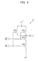
- FIG. 9 is a circuit diagram showing a conventional 2-input NAND element
- FIG. 10 is a circuit diagram showing a conventional 3-input NAND element
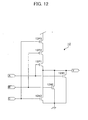
- FIG. 11 is a circuit diagram showing a conventional 2-input NOR element
- FIG. 12 is a circuit diagram showing a conventional 3-input NOR element.
- SET single event transient
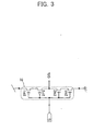
- FIG. 3 is a circuit diagram showing an inverter 2I with a redundant or double structure. Specifically, in the inverter 2I, a first p-channel MOS transistor 2P1 and a first n-channel MOS transistor 2N1 are connected in series with respect to a source or drain line in this order in a direction from a node connected to the side of a first voltage source to a node connected to the side of a second voltage source.
- a second p-channel MOS transistor 2P2 and a second n-channel MOS transistor 2N2 are connected, respectively, to the first p-channel MOS transistor 2P1 and the first n-channel MOS transistor 2N1 through respective gates thereof, and connected in series with respect to the source or drain line, to form a double structure.
- the above inverter 2I can suppress SEE to some extent.
- a clock signal G has a high level
- each of the transistors 2P1, 2P2 is in an OFF state
- each of the transistors 2N1, 2N2 is in an ON state.
- an inverted clock signal GBi, or output has a low level. Given that either one of the transistors 2P1, 2P2 in the OFF state is changed to an ON state due to SEE caused by incident high-energy particles. In this case, the remaining one of the other transistors 2P1, 2P2 connected in series with respect to the source or drain is maintained in the OFF state.
- FIG. 4 is a diagram showing the configuration of an inverter 3I including a double-structured transistor .
- a (p-channel MOS) transistor 3P1 corresponding to the transistor 1P1 in the inverter 1I1 is combined with a (p-channel MOS) transistor 3P2 having a channel of the same conductive type as that thereof (p-channel MOS) and a gate connected to a gate thereof, in such a manner that they are connected in series with respect to a source or drain line, so as to form a double structure.
- the two transistors 3P1, 3P2 have a common gate, and their source or drain line to be controlled by the gate are connected in series with each other. Thus, the two transistors have the same operation as that of a single transistor.
- an (n-channel MOS) transistor 3N2 is additionally connected in series to an (n-channel MOS) transistor 3N1 with respect to the source or drain line.
- connection between the nodes A, B will hereinafter be referred to as "AB short line".
- a connection point (downward-sloping slant line in FIG. 4 ) from a first voltage supply having a voltage supply voltage V DD is connected to the transistor 3P1
- a connection point (downward-sloping slant line in FIG. 4 ) from a second voltage supply having a voltage supply voltage Vss (symbol of Chassis Ground) is connected to the transistor 3N1.
- Vss is set at 0 (zero) V.
- the operation of the inverter 3I Firstly, the operation will be described under the condition that a clock signal G is in a high level.
- the transistors 3P1 and transistor 3P2 are in their OFF state, and the transistors 3N1 and transistor 3N2 are in their ON state.
- an inverted clock signal GBi has a low level.
- the node A is in a low level, and a potential difference between the source and drain of the transistor 3P2 becomes approximately zero. It has been proven that the inverter 3I can effectively prevent SEE. It is believed that this effect is obtained from the following mechanism.
- SEE occurs when a transistor in its OFF state is turned on due to SEE. That is, SEE is likely to occur in the transistors 3P1, 3P2 in the OFF state.
- the transistor 3P2 includes approximately no region with a strong electric field therein, because of approximately zero potential difference between the source and drain thereof, as described above.
- SEE transient current flow
- the operation will be described under the condition that the clock signal G is in a low level.
- the transistors 3P1 and transistor 3P2 are in the ON state, and the transistors 3N1 and transistor 3N2 are in the OFF state.
- a potential difference between the source and drain of the transistor 3N2 becomes approximately zero due to the shout line AB. This allows the transistor 3N2 to have almost no region with a high electric field therein, so as to be less subject to SEE.
- this inverter 3I is configured to allow each of the transistors themselves as components to be less subject to SEE. Further, even if SEE occurs therein, almost no adverse effect will reach an output of the inverter 3I. This makes it possible to provide enhanced SEE tolerance to the inverter 3I.
- FIG. 7 is a sectional view of an SOI-substrate n-channel MOS transistor 30.
- a body p region 34
- SiO 2 insulating film 35 a SiO 2 insulating film 35.
- FIG. 8 is a sectional view of a bulk-substrate n-channel MOS transistor 40.
- This substrate does not have any insulating film as in the SOI substrate.
- a p-type substrate 46 its voltage is kept at Vss.
- a high-level voltage is applied to source 41-drain 43 of the n-channel MOS transistor in its OFF state, a PN junction region is reversely biased, and a high electric field region 47 will be formed. This would involve the risk of occurrence of SEE between the source/drain and substrate.
- the present invention may be implemented using a bulk substrate as well as an SOI substrate, it is desirable to use an SOI substrate.
- a memory element can be obtained by cross-connecting respective outputs and inputs of two inverters directly or indirectly through a switching gate.
- a memory element with such a storage node includes a SRAM (Static RAM), a flip-flop circuit and a latch circuit.
- the memory element has a storage node comprising at least two inverters each having the same configuration as that of the inverter 3I . This makes it possible to achieve a memory element having enhanced SEE tolerance.
- each of the inverters forming the storage mode has the same operation as that of the inverter 3I.
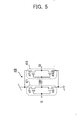
- FIG. 6 is a circuit diagram of the data latch circuit 4.
- a buffer circuit 4B illustrated in FIG. 5 is used in combination with the data latch circuit 4 to shape a waveform of a clock signal G and an inverted clock signal GBi which are input into the data latch circuit 4.
- the buffer circuit 4B includes an inverter 4I1 and an inverter 4I2 which are connected to each other in a cascade arrangement. Viewed as a whole, the buffer circuit 4B generally comprises a clocked inverter 413 serving as an input stage, a transmission gate 4S1, the inverter 4I4 and the inverter 4I2.
- the clocked inverter 4I1 comprises a p-channel MOS transistor 4P3, a p-channel MOS transistor 4P4, a p-channel MOS transistor 4P5, an n-channel MOS transistor 4N5, an n-channel MOS transistor 4N4 and an n-channel MOS transistor 4N3, which are connected in series with respect to a source or drain line in this order in a direction from a node connected to the side of a first voltage supply to a second voltage supply.
- a clock signal Gi and an inverted clock signal which are complementary clock signals are input, respectively, into a first gate group of respective gates of the p-channel MOS transistor 4P3 and the p-channel MOS transistor 4P5, and a second gate group of respective gates of the n-channel MOS transistor 4N3 and the n-channel MOS transistor 4N5.
- a conventional clocked inverter comprises total four transistors consisting of two p-channel MOS transistors and two n-channel MOS transistors
- this clocked inverter 4I1 comprises total six transistors consisting of three p-channel MOS transistors and three n-channel MOS transistors.
- a first transistor having a gate connected to an input data signal D is sandwiched between two second and third transistors connected, respectively, on upper and lower sides of the first transistor.
- the clock signal Gi or the inverted clock signal GBi is connected to each of the second and third transistors.
- the clocked inverter 413 is operable, when the inverted clock signal GBi is in a high level, to invert the input data signal D and output the inverted signal to a transmission date 4S1 (inversion and then conduction). Further, when the inverted clock signal GBi is in a low level, an output terminal of the clocked inverter 413 is placed in a high impedance state (non-conduction).
- the transmission gate 4S1 comprises a p-channel MOS transistor 4P6 and an n-channel MOS transistor 4N6 which are connected in parallel with each other.
- the inverted clock signal GBi is input into a gate of the transistor 4P6, and the clock signal Gi is input into a gate of the transistor 4N6.
- the transmission gate 4S1 is designed to be turned off (non-conduction, high impedance state) when the inverted clock signal Bi is in the high level, and turned on (conduction) when the inverted clock signal Bi is in the low level. As to the clock signal G, this operation is opposite in phase to that of the clocked inverter 4I1.
- inverter 4I3 and the transmission gate 4S1 have a common logic value of the clock signal G, when one of them is in a conduction state, the other is in a non-conduction state.
- Either one of inverters 4I4, 4I5 may be designed as a clocked inverter to integrate the transmission gate 4S1 therewith.
- the inverter 4I4 has an input connected to an output of the inverter 4I5, and an output connected to an output of the clocked inverter 4I3 and an input of the inverter 4I5, through the transmission gate 4S1.
- the output of the inverter 4I4 is also output to a connection point of an inverted output data signal XQ as an output of the data latch circuit 4.
- the inverter 4I4 has the same configuration as that of the SEE tolerant inverter 3I.
- the inverter 4I5 receives an output from the clocked inverter 4I3, and outputs a resulting signal to a connection point of an output data signal Q and an input of the inverter 4I4.
- the output of the inverter 4I5 is also output to the connection point of the output data signal Q as an output of the data latch circuit 4.
- the inverter 5I5 has the same configuration as that of the SEE tolerant inverter 3I.
- the clocked inverter 413 Inverts an input data signal D and outputs the inverted input signal to the subsequent stage.
- the transmission gate 4S1 is in its OFF state, and thereby the output of the clocked inverter 4I3 is not transmitted to the input of the inverter 4I4.
- the output of the clocked inverter 4I3 is transmitted to the input of the inverter 4I5.
- this transmitted data is inverted to have the same logic value as that of the corresponding input data, and output as the output data Q. This output is also input into the inverter 4I4.
- this output is inverted to have a logic value opposite to that of the input data signal D, and output as the inverted output data signal XQ.
- the output data Q is output as a signal having the same logic level as that of the input data signal (transparent mode, through mode).
- the output of the clocked inverter 4I3 is placed in the high impedance state and no input data signal will be output to the subsequent stages.
- the transmission gate 4S1 is changed from the OFF state to the ON state to allow the output of the inverter 4I1 having the same logic value as that of the input data signal D to be passed therethrough, and transmitted to the inverter 4I4.
- the inverter 4I1 inverts the transmitted data to have a logic level opposite to that of the input data signal D, and transmits the inverted data to an input of the inverter 4I5.
- the inverter 415 respective logic levels of the input and the output are opposite to each other, and this state is stably held in the storage node composed of the inverter 4I1 and 4I5. Then, the storage node outputs the output data signal Q having the same logic level as the input data signal at a time of rising edge of the output data signal Q (latch mode). This state will be continued until the clock signal has a low level.
- each of these inverters consists of the SEE tolerant inverter.
- the storage node can effectively prevent the occurrence of SEE. This makes it possible to effectively prevent the inversion of stored data which would otherwise occur in this storage node by SEE.
- the risk of SEE has to be considered, particularly in a state when the data latch circuit 4 is in the latch state, and the output of clocked inverter 4I3 is in the high impedance state.
- each of the four transistors each having a gate connected with the clock signal G and the inverted clock signal GBi is in the OFF state. If one of the transistors is turned on due to SEE, it is likely that the clocked inverter 4I3 momentarily outputs the input data signal D (after inverting) to the subsequent stage. If this input data signal D has a logic level opposite to a logic state stored on the storage node, the stored data will be inverted (occurrence of SEE).
- the clocked inverter 4I3 In the latch mode, the clocked inverter 4I3 according to the present invention can effectively prevent the input data signal D from adversely affecting the subsequent stages, based on the following mechanism.
- the clocked inverter 4I3 comprises the six transistors consisting of the three p-channel MOS transistors and three n-channel MOS transistors. In each of the p-channel and n-channel MOS transistor groups, the first transistor having the gate connected to the input data signal D is sandwiched between the two second and third transistors connected, respectively, on upper and lower sides of the first transistor. In the latch state, the transistor 4P3 and the transistor 4P5 are in the OFF state. Thus, the input data signal D is blocked, and prevented from being output to the subsequent stages.
- the transistor 4P3 and the transistor 4P5 can be arranged instead of the above arrangement of sandwiching the transistor 4P4 therebetween.
- the transistor 4P3 and the transistor 4P5 may be connected in series in adjacent relation to each other, and then connected to the transistor 4P4 on the side of the first voltage source, or may be connected in series in adjacent relation to each other, and then connected to the side of the second voltage source. Even if either one of the transistors is turned on due to SEE, this arrangement can also prevent an adverse effect of the input data signal D from being output to the subsequent stages, as long as the remaining transistor is kept in the OFF state.
- a distance between respective gates of the transistor 4P3 and the transistor 4P5 can be increased.
- the increased inter-gate distance can significantly lower the probability that just one attack of high-energy particles simultaneously causes SEE in the two transistors.
- the group of the transistor 4N3, the transistor 4N4 and the transistor 4N5 has the same effect.
- two transistors adapted to be controlled by the clock are arranged, respectively, on both sides of a transistor adapted to receive input data signal D.
- FIG. 13 is a circuit diagram of the 2-input NAND element 13.
- the 2-input NAND element 13 comprises: a pair of a first p-channel MOS transistor 13P1 and a second p-channel MOS transistor 13P2 which have channels connected in parallel with each other; and a pair of a first n-channel MOS transistor 13N1 and a second n-channel MOS transistor 13N1 which have channels connected in series with each other.
- the p-channel MOS transistor pair (13P1, 13P2) and the n-channel MOS transistor pair (13N1, 13N2) are formed on a substrate having an SOI structure, and connected in series in a direction from a node connected to the side of a first voltage source to a node connected to the side of a second voltage source.
- Respective gates of the first p-channel MOS transistor 13P1 and the first n-channel MOS transistor 13N1 are connected to a first input A
- respective gates of the second p-channel MOS transistor 13P2 and the second n-channel MOS transistor 13N2 are connected to a second input B.
- a node between the p-channel MOS transistor pair (13P1, 13P2) and the n-channel MOS transistor pair (13N1, 13N2) is connected to an output Y.
- Each of the first p-channel MOS transistor 13P1, the second p-channel MOS transistor 13P2, the first n-channel MOS transistor 13N1 and the second n-channel MOS transistor 13N2, is combined with an additional MOS transistor (13P3, 13P4, 13N1, 13N4) having a channel of the same conductive type as that thereof and a gate interconnected to a gate thereof, in such a manner that their channels are connected in series.
- the 2-input NAND element 13 is formed as an SEE tolerant SOI-based 2-input NAND element with a double structure.
- two of the additional n-channel MOS transistor 13N3, 13N4 combined, respectively, with the first n-channel MOS transistor 13N1 and the second n-channel MOS transistor 13N2 through their series-connected channels for forming the double structure, are connected thereto except for a position between the first and second n-channel MOS transistors 13N1, 13N2.
- the additional transistor can be arranged at a position distant from the other transistor. This makes it possible to prevent both the double-structured transistors from being simultaneously turned on due to attack of high-energy particles, so as to achieve further enhanced SEE tolerance.
- the output Y is shifted from the high level to a low level, or a logic value is inverted, resulting in occurrence of SEE.
- the pair of p-channel MOS transistors 13P1, 13P3, the pair of n-channel MOS transistors 13N1, 13N3, the pair of p-channel MOS transistors 13P2, 13P4 and the pair of n-channel MOS transistor 13N2, 13N4 in the 2-input NAND element 13 are changed, respectively, to an OFF state, ON state, ON state and OFF state, and the output Y has a high level.
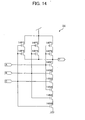
- FIG. 14 is a circuit diagram of the 3-input NAND element 14.
- the 3-input NAND element comprises: a group of a first p-channel MOS transistor 14P1, a second p-channel MOS transistor 14P2 and a third p-channel MOS transistor 14P3 which have channels connected in parallel with each other; and a group of a first n-channel MOS transistor 14N1 a second n-channel MOS transistor 14N2 and a third n-channel MOS transistor 14N3 which have channels connected in series with each other.
- the p-channel MOS transistor group (14P1, 14P2, 14P3) and the n-channel MOS transistor group (14N1, 14N2, 14N3) are formed on a substrate having an SOI structure, and connected in series in a direction from a node connected to the side of a first voltage source to a node connected to the side of a second voltage source.
- Respective gates of the first p-channel MOS transistor 14P1 and the first n-channel MOS transistor 14N1 are connected to a first input A
- respective gates of the second p-channel MOS transistor 14P2 and the second n-channel MOS transistor 14N2 are connected to a second input B.
- respective gates of the third p-channel MOS transistor 14P3 and the third n-channel MOS transistor 14N3 are connected to a third input C, and a node between the p-channel MOS transistor group (14P1, 14P2, 14P3) and the n-channel MOS transistor group (14N1, 14N2, 14N3) is connected to an output Y.
- Each of the first p-channel MOS transistor 14P1, the second p-channel MOS transistor 14P2, the third p-channel MOS transistor 14P3, the first n-channel MOS transistor 14N1, the second n-channel MOS transistor 14N2 and the third n-channel MOS transistor 14N3, is combined with an additional MOS transistor (14P4, 14P5, 14P6, 14N4, 14N5, 14N6) having a channel of the same conductive type as that thereof and a gate interconnected to a gate thereof, in such a manner that their channels are connected in series.
- the 3-input NAND element 14 is formed as, so as to form an SEE tolerant SOI-based 3-input NAND element with a double structure.
- the three additional n-channel MOS transistor (14N4, 14N5, 14N6) combined, respectively, with the first n-channel MOS transistor 14N1, the second n-channel MOS transistor 14N2 and the third n-channel MOS transistor 14N3 through their series-connected channels for forming the double structure, are connected thereto except for a position between any two of the first, second and third n-channel MOS transistors 14N1, 14N2, 14N3.
- the additional transistor can be arranged at a position distant from the other transistor. This makes it possible to prevent both the double-structured transistors from being simultaneously turned on due to attack of high-energy particles, so as to achieve further enhanced SEE tolerance.
- FIG. 10 An operation of the 3-input NAND element 14 will be described in comparison with a conventional 3-input NAND element 10 illustrated in FIG. 10 .
- the input A, the input B and the input C are, respectively, in a high level, in a high level and in a low level.
- a p-channel MOS transistor 10P1, an n-channel MOS transistor 10N1, a p-channel MOS transistor 10P2, an n-channel MOS transistor 10N2, a p-channel MOS transistor 10P3 and an n-channel MOS transistor 10N3 in the conventional 3-input NAND element 10 are changed, respectively, to an OFF state, ON state, OFF state, ON state, ON state and OFF state, and the output Y has a high level.
- the output Y is shifted from the high level to a low level, or a logic value is inverted, resulting in occurrence of SEE.
- the pair of p-channel MOS transistors 14P1, 14P4, the pair of n-channel MOS transistors 14N1, 14N4, the pair of p-channel MOS transistors 14P2, 14P5, the pair of n-channel MOS transistor 14N2, 14N5, the pair of p-channel MOS transistors 14P3, 14P6 and the pair of n-channel MOS transistor 14N3, 14N6, in the 3-input NAND element 14 are changed, respectively, to an OFF state, ON state, OFF state, ON state, ON state and OFF state, and the output Y has a high level.
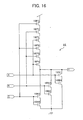
- FIG. 15 is a circuit diagram of the 2-input NOR element 15.
- the 2-input NOR element 15 comprises: a pair of a first p-channel MOS transistor 15P1 and a second p-channel MOS transistor 15P2 which have channels connected in series with each other; and a pair of a first n-channel MOS transistor 15N1 and a second n-channel MOS transistor 15N2 which have channels connected in parallel with each other.
- the p-channel MOS transistor pair (15P1, 15P2) and the n-channel MOS transistor pair (15N1, 15N2) are formed on a substrate having an SOI structure, and connected in series in a direction from a node connected to the side of a first voltage source to a node connected to the side of a second voltage source.
- Respective gates of the first p-channel MOS transistor 15P1 and the first n-channel MOS transistor 15N1 are connected to a first input A
- respective gates of the second p-channel MOS transistor 15P2 and the second n-channel MOS transistor 15N2 are connected to a second input B.
- a node between the p-channel MOS transistor pair (15P1, 15P2) and the n-channel MOS transistor pair (15N1, 15N2) is connected to an output Y.
- Each of the first p-channel MOS transistor 15P1, the second p-channel MOS transistor 15P2, the first n-channel MOS transistor 15N1 and the second n-channel MOS transistor 15N2, is combined with an additional MOS transistor (15P3, 15P4, 15N1, 15N4) having a channel of the same conductive type as that thereof and a gate interconnected to a gate thereof, in such a manner that their channels are connected in series.
- the 2-input NOR element 15 is formed as an SEE tolerant SOI-based 2-input NOR element with a double structure.
- the additional transistor in the 2-input NOR element 15, two of the additional p-channel MOS transistor (15P3, 15P4) combined, respectively, with the first p-channel MOS transistor 15P1 and the second p-channel MOS transistor 15P2 through their series-connected channels for forming the double structure, are connected thereto except for a position between the first and second p-channel MOS transistors 15P1, 15P2.
- the additional transistor in each pair of series-connected or p-channel transistors forming a double structure, the additional transistor can be arranged at a position distant from the other transistor. This makes it possible to prevent both the double-structured transistors from being simultaneously turned on due to attack of high-energy particles, so as to achieve further enhanced SEE tolerance.
- the output Y is shifted from the low level to a high level, or a logic value is inverted, resulting in occurrence of SEE.
- the pair of p-channel MOS transistors 15P1, 15P3, the pair of n-channel MOS transistors 15N1, 15N3, the pair of p-channel MOS transistors 15P2, 15P4 and the pair of n-channel MOS transistor 15N2, 15N4 in the 2-input NOR element 15 are changed, respectively, to an OFF state, ON state, ON state and OFF state, and the output Y has a low level.
- FIG. 16 is a circuit diagram of the 3-input NOR element 16.
- the 3-input NOR element comprises: a group of a first p-channel MOS transistor 16P1, a second p-channel MOS transistor 16P2 and a third p-channel MOS transistor 16P3 which have channels connected in series with each other; and a group of a first n-channel MOS transistor 16N1 a second n-channel MOS transistor 16N2 and a third n-channel MOS transistor 16N3 which have channels connected in parallel with each other.
- the p-channel MOS transistor group (16P1, 16P2, 16P3) and the n-channel MOS transistor group (16N1, 16N2, 16N3) are formed on a substrate having an SOI structure, and connected in series in a direction from a node connected to the side of a first voltage source to a node connected to the side of a second voltage source. Respective gates of the first p-channel MOS transistor 16P1 and the first n-channel MOS transistor 16N1 are connected to a first input A, and respective gates of the second p-channel MOS transistor 16P2 and the second n-channel MOS transistor 16N2 are connected to a second input B.
- respective gates of the third p-channel MOS transistor 16P3 and the third n-channel MOS transistor 16N3 are connected to a third input C, and a node between the p-channel MOS transistor group (16P1, 16P2, 16P3) and the n-channel MOS transistor group (16N1, 16N2, 16N3) is connected to an output Y.
- Each of the first p-channel MOS transistor 16P1, the second p-channel MOS transistor 16P2, the third p-channel MOS transistor 16P3, the first n-channel MOS transistor 16N1, the second n-channel MOS transistor 16N2 and the third n-channel MOS transistor 16N3, is combined with an additional MOS transistor (16P4, 16P5, 16P6, 16N4, 16N5, 16N6) having a channel of the same conductive type as that thereof and a gate interconnected to a gate thereof, in such a manner that their channels are connected in series.
- the 3-input NOR element 16 is formed as, so as to form an SEE tolerant SOI-based 3-input NOR element with a double structure.
- the three additional p-channel MOS transistor (16P4, 16P5, 16P6) combined, respectively, with the first p-channel MOS transistor 16P1, the second p-channel MOS transistor 16P2 and the third p-channel MOS transistor 16P3 through their series-connected channels for forming the double structure, are connected thereto except for a position between any two of the first, second and third n-channel MOS transistors 16P1, 16P2, 16P3.
- the additional transistor can be arranged at a position distant from the other transistor. This makes it possible to prevent both the double-structured transistors from being simultaneously turned on due to attack of high-energy particles, so as to achieve further enhanced SEE tolerance.
- FIG. 12 An operation of the 3-input NOR element 16 will be described in comparison with a conventional 3-input NOR element 12 illustrated in FIG. 12 .
- the input A, the input B and the input C are, respectively, in a high level, in a low level and in a low level.
- a p-channel MOS transistor 12P1, an n-channel MOS transistor 12N1, a p-channel MOS transistor 12P2, an n-channel MOS transistor 12N2, a p-channel MOS transistor 12P3 and an n-channel MOS transistor 12N3 in the conventional 3-input NOR element 12 are changed, respectively, to an OFF state, ON state, ON state, OFF state, ON state and OFF state, and the output Y has a low level.
- the output Y is shifted from the low level to a high level, or a logic value is inverted, resulting in occurrence of SEE.
- the pair of p-channel MOS transistors 16P1, 16P4, the pair of n-channel MOS transistors 16N1, 16N4, the pair of p-channel MOS transistors 16P2, 16P5, the pair of n-channel MOS transistor 16N2, 16N5, the pair of p-channel MOS transistors 16P3, 16P6 and the pair of n-channel MOS transistor 16N3, 16N6, in the 3-input NOR element 16 are changed, respectively, to an OFF state, ON state, ON state, OFF state, ON state and OFF state, and the output Y has a low level.
Landscapes
- Physics & Mathematics (AREA)
- Engineering & Computer Science (AREA)
- Computer Hardware Design (AREA)
- Computing Systems (AREA)
- General Engineering & Computer Science (AREA)
- Mathematical Physics (AREA)
- Logic Circuits (AREA)
- Thin Film Transistor (AREA)
- Semiconductor Memories (AREA)
- Semiconductor Integrated Circuits (AREA)
- Metal-Oxide And Bipolar Metal-Oxide Semiconductor Integrated Circuits (AREA)
Claims (1)
- Circuit de verrouillage de données à base de SOI tolérant aux effets de particules isolées (4), qui est formé sur un substrat ayant une structure SOI et comprenant un premier inverseur (4I5), un deuxième inverseur (4I4) et un inverseur cadencé (4I3), dans lequel :ledit premier inverseur (4I5) a une sortie connectée à une entrée dudit deuxième inverseur (4I4) ;ledit deuxième inverseur (4I4) a une sortie connectée à une entrée dudit premier inverseur (4I5) ; etledit inverseur cadencé (4I3) peut être utilisé pour inverser un signal d'entrée reçu (D) et envoyer ledit signal d'entrée inversé à l'entrée dudit premier inverseur (4I5), sous le contrôle d'une commande marche-arrêt, fondée sur des premiers signaux d'horloge complémentaires (Gi, GBi) ayant des valeurs logiques complémentaires entre elles,caractérisé en ce que :chaque transistor est formé avec son corps respectif (34) isolé électriquement d'un substrat (36) par un film isolant en SiO2 (35), etledit circuit de verrouillage de données à base de SOI tolérant aux effets de particules isolées (4) comprend une double structure dans laquelle au moins l'un desdits premier et deuxième inverseurs (4I4, 4I5) est un inverseur à base de SOI tolérant aux effets de particules isolées comprenant un premier transistor MOS à canal p (4P7, 4P9) et un premier transistor MOS à canal n (4N7, 4N9), qui sont formés sur un substrat ayant une structure SOI, et connectés en série par rapport à une ligne de source ou de drain, dans cet ordre, dans une direction allant d'un noeud connecté du côté d'une première source de tension vers un noeud connecté du côté d'une deuxième source de tension, chacun dudit premier transistor MOS à canal p (4P7, 4P9) et dudit premier transistor MOS à canal n (4N7, 4N9) étant combiné à un deuxième transistor MOS (4P8, 4P10, 4N8, 4N10) ayant un canal du même type de conduction que le sien et une grille interconnectée à sa grille, de telle sorte qu'ils soient connectés en série par rapport à la ligne de source ou de drain, et que des noeuds respectifs entre lesdits premier et deuxième transistors MOS à canal p (4P7, 4P8, 4P9, 4P10) et entre lesdits premier et deuxième transistors MOS à canal n (4N7, 4N8, 4N9, 4N10) soient directement connectés entre eux,etle deuxième inverseur (4I4) soit un inverseur cadencé soumis à une commande marche-arrêt en fonction de deuxièmes signaux d'horloge complémentaires (Gi, GBi) en opposition de phase par rapport auxdits premiers signaux d'horloge complémentaires (Gi, GBi).
Applications Claiming Priority (2)
| Application Number | Priority Date | Filing Date | Title |
|---|---|---|---|
| JP2004027818 | 2004-02-04 | ||
| EP05709741A EP1720257B1 (fr) | 2004-02-04 | 2005-02-04 | Inverseur, élément de mémoire à semiconducteur et dispositif de verrouillage de données à base de SOI tolérant aux effets d'un seul événement |
Related Parent Applications (2)
| Application Number | Title | Priority Date | Filing Date |
|---|---|---|---|
| EP05709741A Division EP1720257B1 (fr) | 2004-02-04 | 2005-02-04 | Inverseur, élément de mémoire à semiconducteur et dispositif de verrouillage de données à base de SOI tolérant aux effets d'un seul événement |
| EP05709741.2 Division | 2005-02-04 |
Publications (3)
| Publication Number | Publication Date |
|---|---|
| EP2107680A2 EP2107680A2 (fr) | 2009-10-07 |
| EP2107680A3 EP2107680A3 (fr) | 2010-01-13 |
| EP2107680B1 true EP2107680B1 (fr) | 2012-01-25 |
Family
ID=34835905
Family Applications (3)
| Application Number | Title | Priority Date | Filing Date |
|---|---|---|---|
| EP09163916A Ceased EP2107679A3 (fr) | 2004-02-04 | 2005-02-04 | Dispositif logique à base de SOI tolérant aux effets d'un seul événement |
| EP05709741A Ceased EP1720257B1 (fr) | 2004-02-04 | 2005-02-04 | Inverseur, élément de mémoire à semiconducteur et dispositif de verrouillage de données à base de SOI tolérant aux effets d'un seul événement |
| EP09163919A Ceased EP2107680B1 (fr) | 2004-02-04 | 2005-02-04 | Dispositif de verrouillage de données à base de SOI tolérant aux effets d'un seul événement |
Family Applications Before (2)
| Application Number | Title | Priority Date | Filing Date |
|---|---|---|---|
| EP09163916A Ceased EP2107679A3 (fr) | 2004-02-04 | 2005-02-04 | Dispositif logique à base de SOI tolérant aux effets d'un seul événement |
| EP05709741A Ceased EP1720257B1 (fr) | 2004-02-04 | 2005-02-04 | Inverseur, élément de mémoire à semiconducteur et dispositif de verrouillage de données à base de SOI tolérant aux effets d'un seul événement |
Country Status (4)
| Country | Link |
|---|---|
| US (1) | US7504850B2 (fr) |
| EP (3) | EP2107679A3 (fr) |
| JP (2) | JP4639342B2 (fr) |
| WO (1) | WO2005076479A1 (fr) |
Cited By (1)
| Publication number | Priority date | Publication date | Assignee | Title |
|---|---|---|---|---|
| TWI888172B (zh) * | 2024-06-14 | 2025-06-21 | 世界先進積體電路股份有限公司 | 邏輯電路 |
Families Citing this family (38)
| Publication number | Priority date | Publication date | Assignee | Title |
|---|---|---|---|---|
| JPH0790255B2 (ja) | 1992-12-04 | 1995-10-04 | 株式会社三五 | 材料供給装置 |
| US20070162880A1 (en) * | 2006-01-12 | 2007-07-12 | Honeywell International Inc. | Single event transient immune antenna diode circuit |
| US7888959B2 (en) * | 2007-09-19 | 2011-02-15 | International Business Machines Corporation | Apparatus and method for hardening latches in SOI CMOS devices |
| US7411411B1 (en) | 2007-10-19 | 2008-08-12 | Honeywell International Inc. | Methods and systems for hardening a clocked latch against single event effects |
| TWI358902B (en) * | 2007-12-31 | 2012-02-21 | Ind Tech Res Inst | Signal delay circuit |
| EP2685633A3 (fr) | 2008-01-17 | 2014-05-07 | Robust Chip, Inc. | Procédé d'agencement de dispositifs électroniques matériels résistant à une erreur logicielle et cellule logique durcie par rayonnement |
| US20130038348A1 (en) * | 2008-01-17 | 2013-02-14 | Klas Olof Lilja | Layout method for soft-error hard electronics, and radiation hardened logic cell |
| US20140157223A1 (en) * | 2008-01-17 | 2014-06-05 | Klas Olof Lilja | Circuit and layout design methods and logic cells for soft error hard integrated circuits |
| US20100019351A1 (en) * | 2008-07-28 | 2010-01-28 | Albert Ratnakumar | Varactors with enhanced tuning ranges |
| US7920410B1 (en) * | 2009-02-23 | 2011-04-05 | Altera Corporation | Memory elements with increased write margin and soft error upset immunity |
| CN102064680B (zh) * | 2009-11-18 | 2013-07-24 | 上海华虹Nec电子有限公司 | 应用于多电源片上系统的混合型锁存器 |
| US8638594B1 (en) | 2009-12-02 | 2014-01-28 | Altera Corporation | Integrated circuits with asymmetric transistors |
| US9496268B2 (en) | 2009-12-02 | 2016-11-15 | Altera Corporation | Integrated circuits with asymmetric and stacked transistors |
| US8482963B1 (en) | 2009-12-02 | 2013-07-09 | Altera Corporation | Integrated circuits with asymmetric and stacked transistors |
| US8138797B1 (en) | 2010-05-28 | 2012-03-20 | Altera Corporation | Integrated circuits with asymmetric pass transistors |
| CN102361442B (zh) * | 2011-10-21 | 2012-12-19 | 中国人民解放军国防科学技术大学 | 抗单粒子翻转的可复位d触发器 |
| CN102394600B (zh) * | 2011-10-21 | 2013-12-11 | 中国人民解放军国防科学技术大学 | 一种抗单粒子翻转的可置位和复位d触发器 |
| CN102361441B (zh) * | 2011-10-21 | 2013-01-02 | 中国人民解放军国防科学技术大学 | 抗单粒子翻转可置位的扫描结构d触发器 |
| CN102361443B (zh) * | 2011-10-21 | 2013-03-27 | 中国人民解放军国防科学技术大学 | 抗单粒子翻转可复位的扫描结构d触发器 |
| CN102394596B (zh) * | 2011-10-21 | 2013-12-11 | 中国人民解放军国防科学技术大学 | 抗单粒子翻转的可置位d触发器 |
| CN102394602B (zh) * | 2011-10-21 | 2013-12-11 | 中国人民解放军国防科学技术大学 | 一种抗单粒子翻转可置位和复位的扫描结构d触发器 |
| CN102394599B (zh) * | 2011-10-21 | 2013-12-11 | 中国人民解放军国防科学技术大学 | 抗单粒子翻转可置位和复位的扫描结构d触发器 |
| CN102394635A (zh) * | 2011-10-28 | 2012-03-28 | 电子科技大学 | 冗余soi电路单元 |
| WO2013082611A2 (fr) | 2011-12-02 | 2013-06-06 | Robust Chip Inc. | Agencement de topologie de circuit électronique résistant aux erreurs intermittentes et cellules logiques |
| WO2014066402A1 (fr) * | 2012-10-22 | 2014-05-01 | Klas Olof Lilja | Procédés de conception de circuit et de topologie et cellules logiques pour circuits intégrés matériels à erreur intermittente |
| US8975928B1 (en) | 2013-04-26 | 2015-03-10 | Altera Corporation | Input-output buffer circuitry with increased drive strength |
| RU2541854C1 (ru) * | 2013-07-16 | 2015-02-20 | Открытое акционерное общество "СТАР" | Функционально-полный толерантный элемент |
| JP5688190B1 (ja) * | 2013-09-03 | 2015-03-25 | ユニサンティス エレクトロニクス シンガポール プライベート リミテッドUnisantis Electronics Singapore Pte Ltd. | 半導体装置 |
| US9519743B1 (en) * | 2014-01-31 | 2016-12-13 | Altera Corporation | Optimal stacked transistor placement to increase single event transient robustness |
| US9997210B2 (en) | 2015-03-27 | 2018-06-12 | Honeywell International Inc. | Data register for radiation hard applications |
| US10305376B1 (en) * | 2015-11-05 | 2019-05-28 | Raytheon Company | Switchable charge pump for multi-mode operation |
| EP3769423B1 (fr) * | 2018-03-19 | 2025-09-10 | Nanyang Technological University | Arrangements de circuit et leurs procédés de formation |
| CN112526301B (zh) * | 2020-11-30 | 2022-01-21 | 广东电网有限责任公司佛山供电局 | 一种高电导率雾下线路冲击耐受特性测试平台及评估方法 |
| KR102295709B1 (ko) * | 2021-02-19 | 2021-08-30 | 한양대학교 산학협력단 | 고속 멀티플렉서 |
| KR20220143272A (ko) * | 2021-04-16 | 2022-10-25 | 삼성전자주식회사 | 직렬 스택 구조의 트랜지스터들을 포함하는 플립 플롭 |
| JP7644970B2 (ja) | 2021-05-19 | 2025-03-13 | 国立研究開発法人宇宙航空研究開発機構 | Cmos回路 |
| JP2023042299A (ja) * | 2021-09-14 | 2023-03-27 | キオクシア株式会社 | 半導体装置 |
| CN120567160B (zh) * | 2025-07-31 | 2025-10-03 | 中国人民解放军国防科技大学 | 利用相反时钟补偿加固的环形振荡器、芯片及电子设备 |
Family Cites Families (16)
| Publication number | Priority date | Publication date | Assignee | Title |
|---|---|---|---|---|
| JPS61206998A (ja) * | 1985-03-11 | 1986-09-13 | Hitachi Ltd | 半導体記憶回路 |
| JPH03108766A (ja) * | 1989-09-22 | 1991-05-08 | Nippondenso Co Ltd | 高耐圧トランジスタ |
| US5175605A (en) * | 1990-02-05 | 1992-12-29 | Rockwell International Corporation | Single event upset hardening circuits, devices and methods |
| JPH0685658A (ja) * | 1992-09-04 | 1994-03-25 | Hitachi Ltd | 多入力論理ゲ−ト回路およびこれを用いた半導体集積回路 |
| JPH0936378A (ja) * | 1995-07-25 | 1997-02-07 | Semiconductor Energy Lab Co Ltd | 半導体装置 |
| JPH118546A (ja) * | 1997-04-24 | 1999-01-12 | Hitachi Ltd | Cmos回路 |
| JP3211773B2 (ja) * | 1998-06-26 | 2001-09-25 | 日本電気株式会社 | 半導体装置およびその製造方法 |
| JP3511908B2 (ja) * | 1998-09-22 | 2004-03-29 | 株式会社日立製作所 | Nmosネットワーク論理回路 |
| US6278287B1 (en) * | 1999-10-27 | 2001-08-21 | The Boeing Company | Isolated well transistor structure for mitigation of single event upsets |
| US6614257B2 (en) * | 2000-05-12 | 2003-09-02 | Bae Systems Information And Electronics Systems Integration, Inc. | Logic architecture for single event upset immunity |
| US20020063583A1 (en) * | 2000-09-29 | 2002-05-30 | Eaton Harry A. | Single event upset immune logic family |
| JP2002200130A (ja) | 2001-01-09 | 2002-07-16 | Kochi Univ Of Technology | 足踏み運動装置 |
| JP2003173681A (ja) * | 2001-12-07 | 2003-06-20 | Mitsubishi Electric Corp | 半導体メモリ回路およびラッチ回路 |
| US6794908B2 (en) * | 2002-05-31 | 2004-09-21 | Honeywell International Inc. | Radiation-hard circuit |
| JP3684210B2 (ja) * | 2002-06-05 | 2005-08-17 | 株式会社東芝 | Cmos出力バッファー回路 |
| JP3718687B2 (ja) | 2002-07-09 | 2005-11-24 | 独立行政法人 宇宙航空研究開発機構 | インバータ、半導体論理回路、スタティックランダムアクセスメモリ、及びデータラッチ回路 |
-
2005
- 2005-02-04 WO PCT/JP2005/001675 patent/WO2005076479A1/fr not_active Ceased
- 2005-02-04 EP EP09163916A patent/EP2107679A3/fr not_active Ceased
- 2005-02-04 JP JP2005517743A patent/JP4639342B2/ja not_active Expired - Fee Related
- 2005-02-04 EP EP05709741A patent/EP1720257B1/fr not_active Ceased
- 2005-02-04 EP EP09163919A patent/EP2107680B1/fr not_active Ceased
-
2006
- 2006-08-03 US US11/499,498 patent/US7504850B2/en not_active Expired - Fee Related
-
2010
- 2010-07-16 JP JP2010161959A patent/JP5414067B2/ja not_active Expired - Lifetime
Cited By (1)
| Publication number | Priority date | Publication date | Assignee | Title |
|---|---|---|---|---|
| TWI888172B (zh) * | 2024-06-14 | 2025-06-21 | 世界先進積體電路股份有限公司 | 邏輯電路 |
Also Published As
| Publication number | Publication date |
|---|---|
| EP2107679A3 (fr) | 2010-01-20 |
| JP5414067B2 (ja) | 2014-02-12 |
| EP2107680A2 (fr) | 2009-10-07 |
| EP1720257A4 (fr) | 2007-08-22 |
| JP4639342B2 (ja) | 2011-02-23 |
| JPWO2005076479A1 (ja) | 2007-10-18 |
| EP1720257A1 (fr) | 2006-11-08 |
| US20070069305A1 (en) | 2007-03-29 |
| JP2011024216A (ja) | 2011-02-03 |
| WO2005076479A1 (fr) | 2005-08-18 |
| EP2107680A3 (fr) | 2010-01-13 |
| US7504850B2 (en) | 2009-03-17 |
| EP1720257B1 (fr) | 2011-08-17 |
| EP2107679A2 (fr) | 2009-10-07 |
Similar Documents
| Publication | Publication Date | Title |
|---|---|---|
| EP2107680B1 (fr) | Dispositif de verrouillage de données à base de SOI tolérant aux effets d'un seul événement | |
| US6327176B1 (en) | Single event upset (SEU) hardened latch circuit | |
| US11177807B2 (en) | Circuit, method for sizing an aspect ratio of transistors of a circuit, and circuit arrangement | |
| JP4332652B2 (ja) | シングルイベント耐性のラッチ回路及びフリップフロップ回路 | |
| JP7283697B2 (ja) | シングルイベントアップセット耐性のラッチ回路及びフリップフロップ回路 | |
| US8324951B1 (en) | Dual data rate flip-flop circuit | |
| US7741877B2 (en) | Circuit for distributing an initial signal with a tree structure, protected against logic random events | |
| CN107342762B (zh) | 一种抗单粒子瞬态时钟树结构 | |
| CN116545418B (zh) | 抗单粒子瞬态和抗单粒子翻转的抗辐射加固触发器电路 | |
| JP2009105967A (ja) | シングルイベント耐性のラッチ回路 | |
| JP5757485B2 (ja) | シングルイベント耐性のラッチ回路 | |
| US6642802B2 (en) | Ring oscillator providing single event transient immunity | |
| US10181851B2 (en) | Dual interlocked logic circuits | |
| US7193451B2 (en) | Method and system for reducing glitch effects within combinational logic | |
| US6078196A (en) | Data enabled logic circuits | |
| Devarapalli et al. | SEU-hardened dual data rate flip-flop using C-elements | |
| US11356094B2 (en) | Circuit arrangements and methods for forming the same | |
| US12294363B2 (en) | Circuit for mitigating single-event-transients | |
| CN119766204B (zh) | 一种抵抗数字电路中单粒子翻转的锁存器及触发器 | |
| US11601119B2 (en) | Radiation hardened flip-flop circuit for mitigating single event transients | |
| CN121150682B (zh) | 一种可控时钟沿时间的低功耗加固模块 | |
| CN119766203B (zh) | 一种抵抗单粒子翻转的锁存器及触发器 | |
| US20260081585A1 (en) | Robust single event upset (seu) tolerant high-performance flip-flop | |
| CN120017014A (zh) | 一种应用于绝缘体上硅工艺的内置滤波抗单粒子翻转触发器结构 |
Legal Events
| Date | Code | Title | Description |
|---|---|---|---|
| PUAI | Public reference made under article 153(3) epc to a published international application that has entered the european phase |
Free format text: ORIGINAL CODE: 0009012 |
|
| AC | Divisional application: reference to earlier application |
Ref document number: 1720257 Country of ref document: EP Kind code of ref document: P |
|
| AK | Designated contracting states |
Kind code of ref document: A2 Designated state(s): FR |
|
| PUAL | Search report despatched |
Free format text: ORIGINAL CODE: 0009013 |
|
| AK | Designated contracting states |
Kind code of ref document: A3 Designated state(s): FR |
|
| 17P | Request for examination filed |
Effective date: 20100601 |
|
| 17Q | First examination report despatched |
Effective date: 20100706 |
|
| GRAP | Despatch of communication of intention to grant a patent |
Free format text: ORIGINAL CODE: EPIDOSNIGR1 |
|
| GRAS | Grant fee paid |
Free format text: ORIGINAL CODE: EPIDOSNIGR3 |
|
| GRAA | (expected) grant |
Free format text: ORIGINAL CODE: 0009210 |
|
| AC | Divisional application: reference to earlier application |
Ref document number: 1720257 Country of ref document: EP Kind code of ref document: P |
|
| AK | Designated contracting states |
Kind code of ref document: B1 Designated state(s): FR |
|
| PLBE | No opposition filed within time limit |
Free format text: ORIGINAL CODE: 0009261 |
|
| STAA | Information on the status of an ep patent application or granted ep patent |
Free format text: STATUS: NO OPPOSITION FILED WITHIN TIME LIMIT |
|
| 26N | No opposition filed |
Effective date: 20121026 |
|
| REG | Reference to a national code |
Ref country code: FR Ref legal event code: TP Owner name: JAPAN AEROSPACE EXPLORATION AGENCY, JP Effective date: 20130207 |
|
| REG | Reference to a national code |
Ref country code: FR Ref legal event code: ST Effective date: 20131031 |
|
| REG | Reference to a national code |
Ref country code: FR Ref legal event code: RN Effective date: 20131112 Ref country code: FR Ref legal event code: D3 Effective date: 20131120 |
|
| PGRI | Patent reinstated in contracting state [announced from national office to epo] |
Ref country code: FR Effective date: 20131120 |
|
| REG | Reference to a national code |
Ref country code: FR Ref legal event code: PLFP Year of fee payment: 12 |
|
| REG | Reference to a national code |
Ref country code: FR Ref legal event code: PLFP Year of fee payment: 13 |
|
| REG | Reference to a national code |
Ref country code: FR Ref legal event code: PLFP Year of fee payment: 14 |
|
| PGFP | Annual fee paid to national office [announced via postgrant information from national office to epo] |
Ref country code: FR Payment date: 20210225 Year of fee payment: 17 |
|
| PG25 | Lapsed in a contracting state [announced via postgrant information from national office to epo] |
Ref country code: FR Free format text: LAPSE BECAUSE OF NON-PAYMENT OF DUE FEES Effective date: 20220228 |