EP2107683A1 - Convertisseur analogique/numérique de recherche binaire asynchrone selon un comparateur - Google Patents
Convertisseur analogique/numérique de recherche binaire asynchrone selon un comparateur Download PDFInfo
- Publication number
- EP2107683A1 EP2107683A1 EP08075253A EP08075253A EP2107683A1 EP 2107683 A1 EP2107683 A1 EP 2107683A1 EP 08075253 A EP08075253 A EP 08075253A EP 08075253 A EP08075253 A EP 08075253A EP 2107683 A1 EP2107683 A1 EP 2107683A1
- Authority
- EP
- European Patent Office
- Prior art keywords
- comparator
- analog
- comparators
- signal
- conversion circuit
- Prior art date
- Legal status (The legal status is an assumption and is not a legal conclusion. Google has not performed a legal analysis and makes no representation as to the accuracy of the status listed.)
- Withdrawn
Links
- 238000006243 chemical reaction Methods 0.000 claims description 22
- 238000000034 method Methods 0.000 claims description 15
- 230000008569 process Effects 0.000 description 8
- 238000013139 quantization Methods 0.000 description 6
- 230000001960 triggered effect Effects 0.000 description 4
- 238000005070 sampling Methods 0.000 description 3
- 238000010586 diagram Methods 0.000 description 2
- 238000012986 modification Methods 0.000 description 2
- 230000004048 modification Effects 0.000 description 2
- 238000001228 spectrum Methods 0.000 description 2
- 238000009825 accumulation Methods 0.000 description 1
- 230000009286 beneficial effect Effects 0.000 description 1
- 238000005457 optimization Methods 0.000 description 1
- 230000001172 regenerating effect Effects 0.000 description 1
- 230000000630 rising effect Effects 0.000 description 1
- 238000010845 search algorithm Methods 0.000 description 1
- 230000003068 static effect Effects 0.000 description 1
Images


Classifications
-
- H—ELECTRICITY
- H03—ELECTRONIC CIRCUITRY
- H03M—CODING; DECODING; CODE CONVERSION IN GENERAL
- H03M1/00—Analogue/digital conversion; Digital/analogue conversion
- H03M1/12—Analogue/digital converters
- H03M1/124—Sampling or signal conditioning arrangements specially adapted for A/D converters
- H03M1/1245—Details of sampling arrangements or methods
- H03M1/125—Asynchronous, i.e. free-running operation within each conversion cycle
-
- H—ELECTRICITY
- H03—ELECTRONIC CIRCUITRY
- H03M—CODING; DECODING; CODE CONVERSION IN GENERAL
- H03M1/00—Analogue/digital conversion; Digital/analogue conversion
- H03M1/002—Provisions or arrangements for saving power, e.g. by allowing a sleep mode, using lower supply voltage for downstream stages, using multiple clock domains or by selectively turning on stages when needed
-
- H—ELECTRICITY
- H03—ELECTRONIC CIRCUITRY
- H03M—CODING; DECODING; CODE CONVERSION IN GENERAL
- H03M1/00—Analogue/digital conversion; Digital/analogue conversion
- H03M1/12—Analogue/digital converters
- H03M1/1235—Non-linear conversion not otherwise provided for in subgroups of H03M1/12
-
- H—ELECTRICITY
- H03—ELECTRONIC CIRCUITRY
- H03M—CODING; DECODING; CODE CONVERSION IN GENERAL
- H03M1/00—Analogue/digital conversion; Digital/analogue conversion
- H03M1/12—Analogue/digital converters
- H03M1/34—Analogue value compared with reference values
- H03M1/36—Analogue value compared with reference values simultaneously only, i.e. parallel type
- H03M1/361—Analogue value compared with reference values simultaneously only, i.e. parallel type having a separate comparator and reference value for each quantisation level, i.e. full flash converter type
-
- H—ELECTRICITY
- H03—ELECTRONIC CIRCUITRY
- H03M—CODING; DECODING; CODE CONVERSION IN GENERAL
- H03M1/00—Analogue/digital conversion; Digital/analogue conversion
- H03M1/12—Analogue/digital converters
- H03M1/34—Analogue value compared with reference values
- H03M1/38—Analogue value compared with reference values sequentially only, e.g. successive approximation type
- H03M1/42—Sequential comparisons in series-connected stages with no change in value of analogue signal
Definitions
- the present invention relates to an analog-to-digital converter architecture, wherein a comparator based asynchronous binary search is used.
- FoM Current state-of-the-art Figure of Merit
- Flash architectures as in WO2008/006751 are often chosen because they offer the largest speed. However, area and power depend exponentially on the resolution since the comparators are often the largest contributor to the overall power consumption. The bits are determined via a parallel search. On the other hand, a low-power SAR-based architecture is presented in patent application W02007088175 .
- a 1-bit folding front-end can for example be used in combination with a flash ADC as presented in patent document US6369726 , reducing the number of comparators.
- An analog to digital conversion circuit comprising a plurality of comparators each having a predetermined threshold and arranged for being fed with a version of a same input signal and whereby at least one comparator is arranged for being fed with a clock signal.
- the at least one comparator is further arranged for controlling or triggering at least one other comparator of the plurality of comparators.
- this plurality of comparators is structured in at least two hierarchical layers and a comparator at the highest hierarchical layer is arranged for being fed with the clock signal.
- a Comparator based Asynchronous Binary Search (CABS) architecture is presented to minimize power consumption.
- the only active circuits needed are dynamic comparators with embedded thresholds.
- the architecture offers a power consumption that is proportional to the sampling frequency.
- the architecture comprises a self-clocked (asynchronous) binary tree of comparators. The input signal is applied in parallel to all comparators as is the case with flash converters, but the clock is applied to the first or root comparator only.
- the architecture of the present invention combines a fast flash architecture with a classical SAR-approach. Typically, in a flash converter, the bits are determined via a parallel search, requiring a lot of power consuming comparators. By using (preferably) a binary search instead of a parallel one, the number of active comparators is reduced and therefore the power consumption.
- the architecture further comprises a delay block and a feedback DAC between two subsequent hierarchical layers.
- a self-clocked chain of comparators (with threshold at zero), with inserted delay blocks, controls a feedback DAC.
- a feedback DAC By using a feedback DAC, a successive approximation process or binary search algorithm may be implemented.
- the comparators at lower hierarchical layers are fed with an input signal being a combination of the input signal and the signal output by the feedback DAC.
- an analog to digital conversion circuit for converting an analog signal into a digital representation with n bits.
- m bits are determined via an architecture comprising a self-clocked chain of comparators with delay blocks controlling a feedback DAC implementing the successive approximation process.
- n-m bits are determined via the CABS architecture.
- a method for converting an analog signal into a digital representation of this analog signal.
- the method comprises the steps of: applying this signal to each comparator of an analog-to-digital conversion circuit, comparing this input signal with the predetermined threshold of an at least one comparator and controlling (triggering) a second comparator based on the comparison in the previous step.
- the analog to digital converter comprises a plurality of comparators each having a predetermined threshold; and whereby at least one comparator of this plurality is fed with a clock signal.
- the plurality of comparators is structured in at least two hierarchical layers and the at least one comparator to which the clock signal is fed, is at higher hierarchical layer then the second comparator.
- the step of comparing yields a binary output signal.
- An unsigned binary code is obtained by taking an OR of all '>' output pins of the activated comparators on each layer of the binary tree.
- this architecture contains 2 n -1 comparators, similar to a flash ADC, but of which, only n comparators are activated during quantization, with n OR encoder functions to determine the outputs. This drastically lowers the power consumption.
- step of comparing yields an output signal that is fed to a feedback DAC, implementing a successive approximation process.
- Binary code is determined.
- the CABS can be read out by taking an OR of all '>' (greater than) output pins of the activated comparators on each layer. This has a beneficial effect on the power consumption.
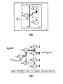
- Fig. 1 represents a block diagram of the present invention.
- Fig. 2 illustrates the proposed CABS binary tree architecture.
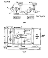
- Fig. 3 illustrates the proposed comparator chain (SAR) architecture.
- Fig. 4 illustrates the architecture of the 2-step 7 bit ADC, 1 bit coarse A/D and D/A followed by a 6 bit CABS ADC.
- Fig. 5 illustrates schematically the clocking.
- Fig. 6 shows the comparator-based asynchronous binary-search operating principle of the 6 bit converter.
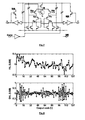
- Fig. 7 shows schematically the circuit of the comparator and the encoder.
- Fig. 8 plots the INUDNL of ADC after calibration.
- Fig. 9 plots the SNDR versus the clock frequency for a low frequency and Nyquist input frequency at different clock rates and the SNDR versus the signal frequency.
- Fig. 10 plots the low frequency and the Nyquist power spectra.
- An analog to digital conversion circuit (1) is presented as shown in Fig.1 , comprising a plurality of comparators (2, 3, 4), preferably structured in layers (10,11) and each having a predetermined threshold. Each comparator is arranged for being fed with a same input signal (5). At least one comparator (2) is arranged for being fed with a clock signal (6), thereby controlling or triggering (7) at least one other comparator (3) of said plurality of comparators (2, 3, 4).
- the clock signal (6) is preferably applied to the comparator (2) of the highest hierarchical layer (10).
- the architecture of the present invention is based on combining a fast flash architecture with a classical SAR-approach.
- the bits are determined via a parallel search, requiring a lot of power consuming comparators.
- a binary search instead of a parallel one, the number of active comparators and therefore the power consumption is reduced.
- the proposed architecture leverages the advantages of both techniques. In other words, an analog-to-digital converter is presented that uses a Comparator based Asynchronous Binary Search (CABS) architecture to minimize power consumption. The only active circuits needed are dynamic comparators with embedded threshold.
- CABS Asynchronous Binary Search
- the architecture offers a power consumption that is proportional to the sampling frequency.
- Fig. 2 The operation of the proposed CABS architecture is exemplified in Fig. 2 .
- the black bold line gives the binary search sequence.
- the sign of the input is determined (> or ⁇ 0).
- the input is compared to half the range and in a third step to 1 ⁇ 4 of the range. Only 3 (or n) comparators need to be activated, instead of 7 (or 2 n -1).
- the clock signal is only applied to the root comparator.
- a comparator of a second level is triggered or controlled by the comparator of the first comparison step.
- the architecture comprises a self-clocked chain of comparators (with threshold at zero) with inserted delay blocks controlling a feedback DAC implementing the successive approximation process or binary search.
- the delay block can be implemented using inverters with limited drive strength. The presence of the delay block provides the feedback DAC some time to adapt to the input signal (15). The settling of the DAC occurs faster than the logic delay time ⁇ .
- Fig. 3 shows the proposed comparator chain for two bits. Again, the clock signal is only applied to the comparator of the highest hierarchical level and a comparator of a second level is triggered by the first comparison step.
- a SAR controller is implemented. The output of the first comparison is fed back to a DAC.
- the input is compared to zero.
- the DAC subtracts 1/2 of the full-scale range in charge from one of the input nodes (0.3 > 0).
- the DAC adds % (-0.2 ⁇ 0) to the input. Note that in this embodiment the SAR approach has been used for reading out the binary code.
- the SAR register is hence formed by the comparator outputs at each layer (to be more precise, by the positive output).
- n bits are determined via an architecture comprising a self-clocked chain of comparators with delay blocks controlling a feedback DAC implementing the successive approximation process.
- n-m bits are determined via the CABS architecture.
- the present invention is illustrated in Fig.4 and provides a 2-step 7 bit ADC comprising a track and hold (T/H) circuit (21), followed by a 1 bit comparison and D/A conversion (22), and a 6 bit comparator-based asynchronous binary-search (CABS) conversion (23), whereby the different blocks are steered by a clock generator (24).
- the 7b ADC operates as follows: the passive T/H circuit (21) samples the input signal (25) on a capacitance (26), the 1 bit comparator (27) determines the sign of the input (MSB, B[6]) and steers a capacitive DAC (28).
- the DAC subtracts 1 ⁇ 4 of the full-scale range in charge from one of the input nodes, changing simultaneously differential signal and common-mode level to be in range of the 6 bit CABS converter (23).
- the clock buffer (24) generates the 1 bit coarse A/D clock signal (29) and starts (30) the 6 bit fine conversion after the 1 bit D/A conversion has finished (31). This clocking is graphically represented in Fig.5 .
- the 6 bit CABS converter comprises a self-clocked (asynchronous) binary tree of comparators with embedded threshold.
- a conceptual block diagram is shown in Fig. 6(a) (for the two MSBs only).
- the input signal is applied in parallel to all comparators as is the case with flash converters, but the clock (30) is applied to the root comparator only.
- This comparator determines if the sampled signal is above or below 0 and outputs this on either its ' ⁇ ' (lower than) for '>' (greater than) pin.
- One of the comparators (3,4) in the next layer of the binary tree is then triggered asynchronously, i.e. either the 1 ⁇ 2 or the -1 ⁇ 2 scale comparator (waveforms shown in Fig. 6(b) ).
- An unsigned binary code is obtained by taking an OR of all '>' output pins of the activated comparators on each layer.
- this architecture contains 2 n -1 comparators, similar to a flash ADC, but of which, only n comparators are activated during quantization, with n OR encoder functions to determine the outputs. This drastically lowers the power consumption.
- a clock signal starts and resets the level-triggered quantization process. Note that in contrast to standard asynchronous SAR implementations, in this architecture a comparator is not reset immediately. Only when the whole quantization process is finished, the n activated comparators are reset from the root comparator following the same path as during quantization. This reset phase overlaps with the tracking phase of the T/H circuit.
- the comparator is implemented using a dynamic latch (see Fig. 7 ), as described for example in " A Current-Controlled Latch Sense Amplifier and a Static Power-Saving Input Buffer for Low-Power Architecture” (T. Kobayashi et al., IEEE J. Solid-State Circuits, vol. 28, no. 4, pp. 523-527, Apr. 1993 ) or in “ Yield and Speed Optimization of a Latch-Type Voltage Sense Amplifier” (B. Wicht et al., IEEE J. Solid-State Circuits, vol. 39, no. 7, pp. 1148-1158, Jul. 2004 ).
- the comparator is reset and both outputs are low.
- the inverter stages at both outputs have a high input threshold to avoid causing a trigger event on both outputs. They also buffer the signal to drive the next comparator in the binary tree and the encoder transistors.
- the OR encoder function is implemented by driving the bitline B[/] (of the ith layer) by a pull-up transistor if the comparator decides 'greater than', and a pull-down transistor if the comparator decides 'lower than'.
- the non-activated comparators on each layer have a high-impedance output. When the comparator is reset, the outputs remain on the bit lines, so the output of the ADC is available after the quantization has finished and the comparators are reset.
- the converter is implemented in a 1 V 90nm digital CMOS using low-and regular-V T devices only.
- the ADC is calibrated as follows : for each comparator the desired threshold is applied at the input and the digital calibration code is found with a binary search where the ADC output toggles 50% between the two codes.
- the capacitive DAC is calibrated similarly, by applying two thresholds and using a comparator to determine when the step is exactly 1 ⁇ 2 of full scale. Both feedback capacitances C in-DA (coarse steps) as well as C in (fine steps) are calibrated in this way ( Fig. 3 ). Once calibrated, the ADC is characterized for different clock frequencies.
- a maximum INL (integral non-linearity) and DNL (differential non-linearity) of 0.48 and 0.93LSB are obtained ( Fig. 8 ) where the LSB size is 6mV.
- the ADC achieves 40dB SNDR over the whole Nyquist band, the Effective Resolution Bandwidth (ERBW) is 270MHz ( Fig. 9 ).
- the power consumption scales linearly with the sampling rate and is equal to 0.89 ⁇ W per MHz of clock rate. This gives a FOM of 10fJ/conversion-step.
- the FOM of the ADC above 100MS/s and for 6 bits and more has been improved from 220fJ to 10fJ/Conversion step.
- the power spectra of a full-scale low-frequency and Nyquist input signal at 150MS/s are shown in Fig. 10 , the Spurious Free Dynamic Range (SFDR) is 55.4dB for a low-frequency.
- SFDR Spurious Free Dynamic Range
- top, bottom, over, under, and the like are introduced for descriptive purposes and not necessarily to denote relative positions. It is to be understood that the terms so used are interchangeable under appropriate circumstances and embodiments of the invention are capable of operating according to the present invention in other sequences, or in orientations different from the one(s) described or illustrated above.
Landscapes
- Engineering & Computer Science (AREA)
- Theoretical Computer Science (AREA)
- Analogue/Digital Conversion (AREA)
Priority Applications (4)
| Application Number | Priority Date | Filing Date | Title |
|---|---|---|---|
| EP08075253A EP2107683A1 (fr) | 2008-03-31 | 2008-03-31 | Convertisseur analogique/numérique de recherche binaire asynchrone selon un comparateur |
| EP09705557A EP2238689B1 (fr) | 2008-01-31 | 2009-01-22 | Convertisseur a/n de recherche binaire asynchrone basée sur comparateur |
| PCT/EP2009/050723 WO2009095349A1 (fr) | 2008-01-31 | 2009-01-22 | Convertisseur a/n de recherche binaire asynchrone basée sur comparateur |
| US12/863,149 US8199043B2 (en) | 2008-01-31 | 2009-01-22 | Comparator based asynchronous binary search A/D converter |
Applications Claiming Priority (1)
| Application Number | Priority Date | Filing Date | Title |
|---|---|---|---|
| EP08075253A EP2107683A1 (fr) | 2008-03-31 | 2008-03-31 | Convertisseur analogique/numérique de recherche binaire asynchrone selon un comparateur |
Publications (1)
| Publication Number | Publication Date |
|---|---|
| EP2107683A1 true EP2107683A1 (fr) | 2009-10-07 |
Family
ID=39590255
Family Applications (2)
| Application Number | Title | Priority Date | Filing Date |
|---|---|---|---|
| EP08075253A Withdrawn EP2107683A1 (fr) | 2008-01-31 | 2008-03-31 | Convertisseur analogique/numérique de recherche binaire asynchrone selon un comparateur |
| EP09705557A Active EP2238689B1 (fr) | 2008-01-31 | 2009-01-22 | Convertisseur a/n de recherche binaire asynchrone basée sur comparateur |
Family Applications After (1)
| Application Number | Title | Priority Date | Filing Date |
|---|---|---|---|
| EP09705557A Active EP2238689B1 (fr) | 2008-01-31 | 2009-01-22 | Convertisseur a/n de recherche binaire asynchrone basée sur comparateur |
Country Status (3)
| Country | Link |
|---|---|
| US (1) | US8199043B2 (fr) |
| EP (2) | EP2107683A1 (fr) |
| WO (1) | WO2009095349A1 (fr) |
Cited By (1)
| Publication number | Priority date | Publication date | Assignee | Title |
|---|---|---|---|---|
| WO2013095085A1 (fr) | 2011-12-20 | 2013-06-27 | Mimos Berhad | Convertisseur analogique-numérique |
Families Citing this family (14)
| Publication number | Priority date | Publication date | Assignee | Title |
|---|---|---|---|---|
| US8849227B2 (en) * | 2009-09-28 | 2014-09-30 | The Trustees Of Columbia University In The City Of New York | Systems and methods for controlling the second order intercept point of receivers |
| JP5269120B2 (ja) | 2011-02-15 | 2013-08-21 | 株式会社東芝 | アナログデジタル変換器 |
| US8446308B2 (en) * | 2011-04-21 | 2013-05-21 | Kabushiki Kaisha Toshiba | Apparatus for detection of a leading edge of a photo sensor output signal |
| US8922415B2 (en) | 2012-08-10 | 2014-12-30 | Maxlinear, Inc. | Method and system for asynchronous successive approximation register (SAR) analog-to-digital converters (ADCs) |
| US8754797B2 (en) * | 2012-08-30 | 2014-06-17 | Texas Instruments Incorporated | Asynchronous analog-to-digital converter having rate control |
| JP5942798B2 (ja) * | 2012-11-12 | 2016-06-29 | 富士通株式会社 | 比較回路およびa/d変換回路 |
| US9184761B2 (en) * | 2013-03-01 | 2015-11-10 | Texas Instruments Incorporated | Asynchronous to synchronous sampling using Akima algorithm |
| JP6098342B2 (ja) * | 2013-05-09 | 2017-03-22 | 株式会社ソシオネクスト | コンパレータ |
| DE102016108081A1 (de) | 2016-05-02 | 2017-11-02 | Denso Corporation | Mikroprozessor mit Zusatz-Befehlen für Binärsuche und zugehöriges Suchverfahren |
| US10862495B1 (en) | 2018-04-17 | 2020-12-08 | Ali Tasdighi Far | Glitch free current mode analog to digital converters for artificial intelligence |
| US10797718B1 (en) | 2018-04-17 | 2020-10-06 | Ali Tasdighi Far | Tiny low power current mode analog to digital converters for artificial intelligence |
| US10833692B1 (en) | 2018-04-17 | 2020-11-10 | Ali Tasdighi Far | Small low glitch current mode analog to digital converters for artificial intelligence |
| KR102536240B1 (ko) | 2019-02-26 | 2023-05-24 | 삼성전자주식회사 | 수신 회로 및 이를 포함하는 근거리 무선 통신 카드 |
| WO2020201850A1 (fr) * | 2019-04-04 | 2020-10-08 | King Abdullah University Of Science And Technology | Configuration d'arbre d'approximations successives pour convertisseur analogique-numérique |
Citations (5)
| Publication number | Priority date | Publication date | Assignee | Title |
|---|---|---|---|---|
| EP1079528A1 (fr) * | 1999-08-25 | 2001-02-28 | Alcatel | Convertisseur analogique/numérique à décisions asynchrones en mode de courant |
| US6369726B1 (en) | 2000-09-13 | 2002-04-09 | Texas Instruments Incorporated | Fast acting polarity detector |
| EP1367720A1 (fr) * | 2002-05-27 | 2003-12-03 | Fujitsu Limited | Circuit de courant de polarisation de convertisseur A/N |
| WO2007088175A1 (fr) | 2006-01-31 | 2007-08-09 | Interuniversitair Microelektronica Centrum (Imec) | Convertisseur analogique/numérique comprenant un dispositif comparateur de tension |
| WO2008006751A1 (fr) | 2006-07-14 | 2008-01-17 | Interuniversitair Microelektronica Centrum (Imec) | Convertisseur a/n d'approximations successives de domaine de charge |
Family Cites Families (3)
| Publication number | Priority date | Publication date | Assignee | Title |
|---|---|---|---|---|
| ATE363767T1 (de) * | 2002-07-31 | 2007-06-15 | Quantum Semiconductor Llc | Verfahren zur seriellen, asynchronen analog- digital wandlung mit dynamisch eingestellter bandbreite |
| KR100541053B1 (ko) * | 2003-02-11 | 2006-01-10 | 삼성전자주식회사 | 프로세스들간의 출력 동기가 보정된 다중 프로세스 a/d컨버터 |
| KR100871828B1 (ko) * | 2007-01-29 | 2008-12-03 | 삼성전자주식회사 | 히스테리시스 특성을 이용한 싱글 슬로프 adc와 그 변환 방법, 및 상기 싱글 슬로프 adc를 구비하는 cmos 이미지 센서 |
-
2008
- 2008-03-31 EP EP08075253A patent/EP2107683A1/fr not_active Withdrawn
-
2009
- 2009-01-22 US US12/863,149 patent/US8199043B2/en active Active
- 2009-01-22 EP EP09705557A patent/EP2238689B1/fr active Active
- 2009-01-22 WO PCT/EP2009/050723 patent/WO2009095349A1/fr not_active Ceased
Patent Citations (5)
| Publication number | Priority date | Publication date | Assignee | Title |
|---|---|---|---|---|
| EP1079528A1 (fr) * | 1999-08-25 | 2001-02-28 | Alcatel | Convertisseur analogique/numérique à décisions asynchrones en mode de courant |
| US6369726B1 (en) | 2000-09-13 | 2002-04-09 | Texas Instruments Incorporated | Fast acting polarity detector |
| EP1367720A1 (fr) * | 2002-05-27 | 2003-12-03 | Fujitsu Limited | Circuit de courant de polarisation de convertisseur A/N |
| WO2007088175A1 (fr) | 2006-01-31 | 2007-08-09 | Interuniversitair Microelektronica Centrum (Imec) | Convertisseur analogique/numérique comprenant un dispositif comparateur de tension |
| WO2008006751A1 (fr) | 2006-07-14 | 2008-01-17 | Interuniversitair Microelektronica Centrum (Imec) | Convertisseur a/n d'approximations successives de domaine de charge |
Non-Patent Citations (3)
| Title |
|---|
| B. WICHT ET AL.: "Yield and Speed Optimization of a Latch-Type Voltage Sense Amplifier", IEEE J. SOLID-STATE CIRCUITS, vol. 39, no. 7, July 2004 (2004-07-01), pages 1148 - 1158, XP011114664, DOI: doi:10.1109/JSSC.2004.829399 |
| JUNGWOOK YANG ET AL: "A current boosting full-flash A/D converter", PROCEEDINGS OF THE INTERNATIONAL SYMPOSIUM ON CIRCUITS AND SYSTEMS. SAN DIEGO, MAY 10 - 13, 1992; [PROCEEDINGS OF THE INTERNATIONAL SYMPOSIUM ON CIRCUITS AND SYSTEMS. (ISCAS)], NEW YORK, IEEE, US, vol. 2, 3 May 1992 (1992-05-03), pages 609 - 612, XP010061262, ISBN: 978-0-7803-0593-9 * |
| T. KOBAYASHI ET AL.: "A Current-Controlled Latch Sense Amplifier and a Static Power-Saving Input Buffer for Low-Power Architecture", IEEE J. SOLID-STATE CIRCUITS, vol. 28, no. 4, April 1993 (1993-04-01), pages 523 - 527, XP000362985, DOI: doi:10.1109/4.210039 |
Cited By (1)
| Publication number | Priority date | Publication date | Assignee | Title |
|---|---|---|---|---|
| WO2013095085A1 (fr) | 2011-12-20 | 2013-06-27 | Mimos Berhad | Convertisseur analogique-numérique |
Also Published As
| Publication number | Publication date |
|---|---|
| EP2238689B1 (fr) | 2012-06-20 |
| EP2238689A1 (fr) | 2010-10-13 |
| US8199043B2 (en) | 2012-06-12 |
| US20100328120A1 (en) | 2010-12-30 |
| WO2009095349A1 (fr) | 2009-08-06 |
Similar Documents
| Publication | Publication Date | Title |
|---|---|---|
| EP2107683A1 (fr) | Convertisseur analogique/numérique de recherche binaire asynchrone selon un comparateur | |
| US8508399B2 (en) | Successive approximation analog to digital converter and method of analog to digital conversion | |
| US8659462B2 (en) | Successive approximation register analog-to-digital converter and analog-to-digital conversion method using the same | |
| Chang et al. | A 12b 50MS/s 2.1 mW SAR ADC with redundancy and digital background calibration | |
| US11784653B2 (en) | Hybrid analog-to-digital converter | |
| KR102803679B1 (ko) | 연속 근사 레지스터 아날로그 디지털 변환기 | |
| Cho et al. | A 9-bit 80 MS/s successive approximation register analog-to-digital converter with a capacitor reduction technique | |
| JP2013510483A (ja) | 容量性分圧器 | |
| US12362759B2 (en) | Time-domain assist for successive approximation ADC | |
| US8547271B2 (en) | Method and apparatus for low power analog-to-digital conversion | |
| Jun et al. | IC Design of 2Ms/s 10-bit SAR ADC with Low Power | |
| CN110808737A (zh) | 用于异步sar-adc的延迟链电路的数字校正方法 | |
| US12107596B2 (en) | Successive approximation register based time-to-digital converter using a time difference amplifier | |
| Fani et al. | A 1-V 5-bit 0.5 GS/s time-based flash ADC in 0.18 µm CMOS technology | |
| CN116743176A (zh) | 一种用于sar型adc的辅助解码dac结构 | |
| Deng et al. | A 8-bit 10MS/s asynchronous SAR ADC with resistor-capacitor array DAC | |
| Ni et al. | A 7.8 fJ/conversion-step 9-bit 400-MS/s single-channel SAR ADC with fast control logic | |
| Tsai et al. | A 10-bit 50-MS/s SAR ADC for dual-voltage domain portable systems | |
| Naveed et al. | Successive-approximation-register ADC Implementation in 180 nm CMOS Technology for Bio-medical Applications | |
| Katic et al. | A sub-mW pulse-based 5-bit flash ADC with a time-domain fully-digital reference ladder | |
| CN113055015A (zh) | 一种低驱动电流需求的模数转换器 | |
| Yan et al. | A 4.5-MS/s 12-bit Vcm self-generated SAR ADC in 130-nm CMOS | |
| Gowrishankar et al. | High Precision SAR ADC Using CNTFET for Internet of Things | |
| CN101286746B (zh) | 功率数字转换器 | |
| Hou et al. | An 8-bit 400-MS/s calibration-free SAR ADC with a pre-amplifier-only comparator |
Legal Events
| Date | Code | Title | Description |
|---|---|---|---|
| PUAI | Public reference made under article 153(3) epc to a published international application that has entered the european phase |
Free format text: ORIGINAL CODE: 0009012 |
|
| AK | Designated contracting states |
Kind code of ref document: A1 Designated state(s): AT BE BG CH CY CZ DE DK EE ES FI FR GB GR HR HU IE IS IT LI LT LU LV MC MT NL NO PL PT RO SE SI SK TR |
|
| AX | Request for extension of the european patent |
Extension state: AL BA MK RS |
|
| AKX | Designation fees paid | ||
| REG | Reference to a national code |
Ref country code: DE Ref legal event code: 8566 |
|
| STAA | Information on the status of an ep patent application or granted ep patent |
Free format text: STATUS: THE APPLICATION IS DEEMED TO BE WITHDRAWN |
|
| 18D | Application deemed to be withdrawn |
Effective date: 20100408 |