EP2108947B1 - Vorrichtung und Verfahren zur Inspektion - Google Patents
Vorrichtung und Verfahren zur Inspektion Download PDFInfo
- Publication number
- EP2108947B1 EP2108947B1 EP08254165.7A EP08254165A EP2108947B1 EP 2108947 B1 EP2108947 B1 EP 2108947B1 EP 08254165 A EP08254165 A EP 08254165A EP 2108947 B1 EP2108947 B1 EP 2108947B1
- Authority
- EP
- European Patent Office
- Prior art keywords
- film
- sample
- specimen
- set forth
- cells
- Prior art date
- Legal status (The legal status is an assumption and is not a legal conclusion. Google has not performed a legal analysis and makes no representation as to the accuracy of the status listed.)
- Not-in-force
Links
- 238000007689 inspection Methods 0.000 title claims description 39
- 238000000034 method Methods 0.000 title claims description 29
- 230000003287 optical effect Effects 0.000 claims description 64
- 238000010894 electron beam technology Methods 0.000 claims description 40
- 239000002245 particle Substances 0.000 claims description 25
- 229910052751 metal Inorganic materials 0.000 claims description 18
- 239000002184 metal Substances 0.000 claims description 18
- 229910052581 Si3N4 Inorganic materials 0.000 claims description 15
- HQVNEWCFYHHQES-UHFFFAOYSA-N silicon nitride Chemical compound N12[Si]34N5[Si]62N3[Si]51N64 HQVNEWCFYHHQES-UHFFFAOYSA-N 0.000 claims description 15
- -1 polyethylene Polymers 0.000 claims description 12
- 238000001514 detection method Methods 0.000 claims description 8
- 230000004044 response Effects 0.000 claims description 7
- 230000001678 irradiating effect Effects 0.000 claims description 6
- 229910052582 BN Inorganic materials 0.000 claims description 5
- PZNSFCLAULLKQX-UHFFFAOYSA-N Boron nitride Chemical compound N#B PZNSFCLAULLKQX-UHFFFAOYSA-N 0.000 claims description 5
- OKTJSMMVPCPJKN-UHFFFAOYSA-N Carbon Chemical compound [C] OKTJSMMVPCPJKN-UHFFFAOYSA-N 0.000 claims description 5
- 239000004698 Polyethylene Substances 0.000 claims description 5
- 239000004642 Polyimide Substances 0.000 claims description 5
- 239000004743 Polypropylene Substances 0.000 claims description 5
- VYPSYNLAJGMNEJ-UHFFFAOYSA-N Silicium dioxide Chemical compound O=[Si]=O VYPSYNLAJGMNEJ-UHFFFAOYSA-N 0.000 claims description 5
- 229910052799 carbon Inorganic materials 0.000 claims description 5
- 229920000573 polyethylene Polymers 0.000 claims description 5
- 229920001721 polyimide Polymers 0.000 claims description 5
- 229920000642 polymer Polymers 0.000 claims description 5
- 229920001155 polypropylene Polymers 0.000 claims description 5
- 229910052814 silicon oxide Inorganic materials 0.000 claims description 5
- 238000010521 absorption reaction Methods 0.000 claims description 4
- 210000004027 cell Anatomy 0.000 description 71
- 239000007788 liquid Substances 0.000 description 37
- 238000001878 scanning electron micrograph Methods 0.000 description 12
- 238000006243 chemical reaction Methods 0.000 description 11
- PCHJSUWPFVWCPO-UHFFFAOYSA-N gold Chemical compound [Au] PCHJSUWPFVWCPO-UHFFFAOYSA-N 0.000 description 10
- 229910052737 gold Inorganic materials 0.000 description 10
- 239000010931 gold Substances 0.000 description 10
- 239000001963 growth medium Substances 0.000 description 10
- 238000003384 imaging method Methods 0.000 description 8
- 239000000126 substance Substances 0.000 description 8
- 238000011109 contamination Methods 0.000 description 7
- XUIMIQQOPSSXEZ-UHFFFAOYSA-N Silicon Chemical compound [Si] XUIMIQQOPSSXEZ-UHFFFAOYSA-N 0.000 description 5
- 230000015572 biosynthetic process Effects 0.000 description 5
- 238000010586 diagram Methods 0.000 description 5
- 239000011521 glass Substances 0.000 description 5
- 238000005086 pumping Methods 0.000 description 5
- 229910052710 silicon Inorganic materials 0.000 description 5
- 239000010703 silicon Substances 0.000 description 5
- 102000016289 Cell Adhesion Molecules Human genes 0.000 description 4
- 108010067225 Cell Adhesion Molecules Proteins 0.000 description 4
- 239000003814 drug Substances 0.000 description 4
- 239000000463 material Substances 0.000 description 4
- 239000000758 substrate Substances 0.000 description 4
- BQCADISMDOOEFD-UHFFFAOYSA-N Silver Chemical compound [Ag] BQCADISMDOOEFD-UHFFFAOYSA-N 0.000 description 3
- 229910052782 aluminium Inorganic materials 0.000 description 3
- 239000000427 antigen Substances 0.000 description 3
- 102000036639 antigens Human genes 0.000 description 3
- 108091007433 antigens Proteins 0.000 description 3
- 238000009434 installation Methods 0.000 description 3
- 230000003993 interaction Effects 0.000 description 3
- 229910052709 silver Inorganic materials 0.000 description 3
- 239000004332 silver Substances 0.000 description 3
- KCXVZYZYPLLWCC-UHFFFAOYSA-N EDTA Chemical compound OC(=O)CN(CC(O)=O)CCN(CC(O)=O)CC(O)=O KCXVZYZYPLLWCC-UHFFFAOYSA-N 0.000 description 2
- 102000018697 Membrane Proteins Human genes 0.000 description 2
- 108010052285 Membrane Proteins Proteins 0.000 description 2
- 102000004142 Trypsin Human genes 0.000 description 2
- 108090000631 Trypsin Proteins 0.000 description 2
- XAGFODPZIPBFFR-UHFFFAOYSA-N aluminium Chemical compound [Al] XAGFODPZIPBFFR-UHFFFAOYSA-N 0.000 description 2
- 238000004380 ashing Methods 0.000 description 2
- 210000000170 cell membrane Anatomy 0.000 description 2
- 238000005229 chemical vapour deposition Methods 0.000 description 2
- 238000000151 deposition Methods 0.000 description 2
- 238000006073 displacement reaction Methods 0.000 description 2
- 239000012530 fluid Substances 0.000 description 2
- 239000007789 gas Substances 0.000 description 2
- 238000005286 illumination Methods 0.000 description 2
- 230000007246 mechanism Effects 0.000 description 2
- 230000000877 morphologic effect Effects 0.000 description 2
- 239000004065 semiconductor Substances 0.000 description 2
- 239000012588 trypsin Substances 0.000 description 2
- 102000000905 Cadherin Human genes 0.000 description 1
- 108050007957 Cadherin Proteins 0.000 description 1
- 102000002029 Claudin Human genes 0.000 description 1
- 108050009302 Claudin Proteins 0.000 description 1
- 102000008186 Collagen Human genes 0.000 description 1
- 108010035532 Collagen Proteins 0.000 description 1
- 102000011799 Desmoglein Human genes 0.000 description 1
- 108050002238 Desmoglein Proteins 0.000 description 1
- 239000004593 Epoxy Substances 0.000 description 1
- 102000016359 Fibronectins Human genes 0.000 description 1
- 108010067306 Fibronectins Proteins 0.000 description 1
- 206010020772 Hypertension Diseases 0.000 description 1
- 102000004310 Ion Channels Human genes 0.000 description 1
- 208000021642 Muscular disease Diseases 0.000 description 1
- 201000009623 Myopathy Diseases 0.000 description 1
- 102000010196 Neuroligin Human genes 0.000 description 1
- 108050001755 Neuroligin Proteins 0.000 description 1
- 102000003800 Selectins Human genes 0.000 description 1
- 108090000184 Selectins Proteins 0.000 description 1
- 102100026383 Vasopressin-neurophysin 2-copeptin Human genes 0.000 description 1
- 238000009825 accumulation Methods 0.000 description 1
- 239000000853 adhesive Substances 0.000 description 1
- 230000001070 adhesive effect Effects 0.000 description 1
- 230000000274 adsorptive effect Effects 0.000 description 1
- 230000002411 adverse Effects 0.000 description 1
- 230000006793 arrhythmia Effects 0.000 description 1
- 206010003119 arrhythmia Diseases 0.000 description 1
- 230000005540 biological transmission Effects 0.000 description 1
- 230000000903 blocking effect Effects 0.000 description 1
- UHYPYGJEEGLRJD-UHFFFAOYSA-N cadmium(2+);selenium(2-) Chemical compound [Se-2].[Cd+2] UHYPYGJEEGLRJD-UHFFFAOYSA-N 0.000 description 1
- 238000004113 cell culture Methods 0.000 description 1
- 239000003153 chemical reaction reagent Substances 0.000 description 1
- 238000004140 cleaning Methods 0.000 description 1
- 229920001436 collagen Polymers 0.000 description 1
- 239000013078 crystal Substances 0.000 description 1
- 210000004748 cultured cell Anatomy 0.000 description 1
- 230000003247 decreasing effect Effects 0.000 description 1
- 201000010064 diabetes insipidus Diseases 0.000 description 1
- 206010012601 diabetes mellitus Diseases 0.000 description 1
- 201000010099 disease Diseases 0.000 description 1
- 208000037265 diseases, disorders, signs and symptoms Diseases 0.000 description 1
- 238000001312 dry etching Methods 0.000 description 1
- 230000005611 electricity Effects 0.000 description 1
- 230000008020 evaporation Effects 0.000 description 1
- 238000001704 evaporation Methods 0.000 description 1
- 239000007850 fluorescent dye Substances 0.000 description 1
- 230000004927 fusion Effects 0.000 description 1
- 229910001385 heavy metal Inorganic materials 0.000 description 1
- 239000001307 helium Substances 0.000 description 1
- 229910052734 helium Inorganic materials 0.000 description 1
- SWQJXJOGLNCZEY-UHFFFAOYSA-N helium atom Chemical compound [He] SWQJXJOGLNCZEY-UHFFFAOYSA-N 0.000 description 1
- 102000006495 integrins Human genes 0.000 description 1
- 108010044426 integrins Proteins 0.000 description 1
- 238000010884 ion-beam technique Methods 0.000 description 1
- 238000004519 manufacturing process Methods 0.000 description 1
- 229910021645 metal ion Inorganic materials 0.000 description 1
- 239000000203 mixture Substances 0.000 description 1
- 239000002105 nanoparticle Substances 0.000 description 1
- 229910052759 nickel Inorganic materials 0.000 description 1
- NJPPVKZQTLUDBO-UHFFFAOYSA-N novaluron Chemical compound C1=C(Cl)C(OC(F)(F)C(OC(F)(F)F)F)=CC=C1NC(=O)NC(=O)C1=C(F)C=CC=C1F NJPPVKZQTLUDBO-UHFFFAOYSA-N 0.000 description 1
- 238000000879 optical micrograph Methods 0.000 description 1
- 230000003204 osmotic effect Effects 0.000 description 1
- 238000005192 partition Methods 0.000 description 1
- 239000004033 plastic Substances 0.000 description 1
- 229920003023 plastic Polymers 0.000 description 1
- 229920000729 poly(L-lysine) polymer Polymers 0.000 description 1
- 229920001296 polysiloxane Polymers 0.000 description 1
- 239000000047 product Substances 0.000 description 1
- AAEVYOVXGOFMJO-UHFFFAOYSA-N prometryn Chemical compound CSC1=NC(NC(C)C)=NC(NC(C)C)=N1 AAEVYOVXGOFMJO-UHFFFAOYSA-N 0.000 description 1
- 230000001681 protective effect Effects 0.000 description 1
- 239000002096 quantum dot Substances 0.000 description 1
- 230000036632 reaction speed Effects 0.000 description 1
- 102000005962 receptors Human genes 0.000 description 1
- 108020003175 receptors Proteins 0.000 description 1
- 238000004626 scanning electron microscopy Methods 0.000 description 1
- 238000007789 sealing Methods 0.000 description 1
- 230000035939 shock Effects 0.000 description 1
- 238000004904 shortening Methods 0.000 description 1
- 238000000638 solvent extraction Methods 0.000 description 1
- 238000005507 spraying Methods 0.000 description 1
- 238000004544 sputter deposition Methods 0.000 description 1
- 230000000638 stimulation Effects 0.000 description 1
- 239000006228 supernatant Substances 0.000 description 1
- 230000007704 transition Effects 0.000 description 1
- 238000007740 vapor deposition Methods 0.000 description 1
Images


Classifications
-
- G—PHYSICS
- G01—MEASURING; TESTING
- G01N—INVESTIGATING OR ANALYSING MATERIALS BY DETERMINING THEIR CHEMICAL OR PHYSICAL PROPERTIES
- G01N23/00—Investigating or analysing materials by the use of wave or particle radiation, e.g. X-rays or neutrons, not covered by groups G01N3/00 – G01N17/00, G01N21/00 or G01N22/00
- G01N23/22—Investigating or analysing materials by the use of wave or particle radiation, e.g. X-rays or neutrons, not covered by groups G01N3/00 – G01N17/00, G01N21/00 or G01N22/00 by measuring secondary emission from the material
- G01N23/2204—Specimen supports therefor; Sample conveying means therefore
-
- H—ELECTRICITY
- H01—ELECTRIC ELEMENTS
- H01J—ELECTRIC DISCHARGE TUBES OR DISCHARGE LAMPS
- H01J37/00—Discharge tubes with provision for introducing objects or material to be exposed to the discharge, e.g. for the purpose of examination or processing thereof
- H01J37/02—Details
- H01J37/20—Means for supporting or positioning the object or the material; Means for adjusting diaphragms or lenses associated with the support
-
- H—ELECTRICITY
- H01—ELECTRIC ELEMENTS
- H01J—ELECTRIC DISCHARGE TUBES OR DISCHARGE LAMPS
- H01J37/00—Discharge tubes with provision for introducing objects or material to be exposed to the discharge, e.g. for the purpose of examination or processing thereof
- H01J37/02—Details
- H01J37/22—Optical, image processing or photographic arrangements associated with the tube
- H01J37/226—Optical arrangements for illuminating the object; optical arrangements for collecting light from the object
- H01J37/228—Optical arrangements for illuminating the object; optical arrangements for collecting light from the object whereby illumination or light collection take place in the same area of the discharge
-
- H—ELECTRICITY
- H01—ELECTRIC ELEMENTS
- H01J—ELECTRIC DISCHARGE TUBES OR DISCHARGE LAMPS
- H01J37/00—Discharge tubes with provision for introducing objects or material to be exposed to the discharge, e.g. for the purpose of examination or processing thereof
- H01J37/26—Electron or ion microscopes; Electron or ion diffraction tubes
- H01J37/28—Electron or ion microscopes; Electron or ion diffraction tubes with scanning beams
-
- H—ELECTRICITY
- H01—ELECTRIC ELEMENTS
- H01J—ELECTRIC DISCHARGE TUBES OR DISCHARGE LAMPS
- H01J2237/00—Discharge tubes exposing object to beam, e.g. for analysis treatment, etching, imaging
- H01J2237/20—Positioning, supporting, modifying or maintaining the physical state of objects being observed or treated
- H01J2237/208—Elements or methods for movement independent of sample stage for influencing or moving or contacting or transferring the sample or parts thereof, e.g. prober needles or transfer needles in FIB/SEM systems
-
- H—ELECTRICITY
- H01—ELECTRIC ELEMENTS
- H01J—ELECTRIC DISCHARGE TUBES OR DISCHARGE LAMPS
- H01J2237/00—Discharge tubes exposing object to beam, e.g. for analysis treatment, etching, imaging
- H01J2237/26—Electron or ion microscopes
- H01J2237/2602—Details
- H01J2237/2605—Details operating at elevated pressures, e.g. atmosphere
- H01J2237/2608—Details operating at elevated pressures, e.g. atmosphere with environmental specimen chamber
-
- H—ELECTRICITY
- H01—ELECTRIC ELEMENTS
- H01J—ELECTRIC DISCHARGE TUBES OR DISCHARGE LAMPS
- H01J2237/00—Discharge tubes exposing object to beam, e.g. for analysis treatment, etching, imaging
- H01J2237/26—Electron or ion microscopes
- H01J2237/28—Scanning microscopes
- H01J2237/2803—Scanning microscopes characterised by the imaging method
- H01J2237/2808—Cathodoluminescence
Definitions
- the present invention relates to an apparatus and method capable of inspecting a specimen held on a film by irradiating the specimen with a primary charged particle beam. More particularly, where the specimen consists of biological cells, the invention relates to observation and inspection of reactions of the cells when a stimulus is given to them.
- a sample containing a specimen to be inspected with an inspection apparatus incorporating SEM capabilities is normally placed in a sample chamber whose inside pressure has been reduced by vacuum pumping.
- the sample placed in the sample chamber which in turn is placed in a reduced-pressure ambient in this way, is irradiated with an electron beam (charged particle beam).
- Secondary signals such as secondary electrons or backscattered electrons produced from the sample in response to the irradiation are detected.
- the sample is exposed to a reduced-pressure ambient. Therefore, moisture evaporates from the sample, so that the cells die. It has been impossible to observe reactions to a stimulus.
- One conceivable method of inspecting a sample using SEM without exposing the sample to a reduced-pressure ambient in this way consists of preparing a sample holder whose opening (aperture) has been sealed off by a film, placing the sample in the holder, and installing the holder in an SEM sample chamber that is placed in the reduced-pressure ambient.
- the inside of the sample holder in which the sample is placed is not evacuated.
- the film that covers the opening formed in the sample holder can withstand the pressure difference between the reduced-pressure ambient inside the SEM sample chamber and the ambient (e.g., atmospheric-pressure ambient) of the inside of the sample holder that is not pumped down. Furthermore, the filmpermits an electron beam to pass therethrough (see patent document 1).
- an electron beam is directed at the sample placed within the sample holder from outside the holder via the film on the holder placed in the SEM sample chamber that is in a reduced-pressure ambient.
- Backscattered electrons are produced from the irradiated sample.
- the backscattered electrons pass through the film on the sample holder and are detected by a backscattered electron detector mounted in the SEM sample chamber. Consequently, an SEM image is derived.
- the sample is sealed in the closed space and so it has been impossible to give a stimulus to cells from outside the sample holder, for example, using a manipulator.
- patent document 2 Examples in which two films of the structure described above are placed opposite to each other with a sample interposed between the films and in which an image is acquired by a transmission electron microscope are described in patent documents 2 and 3. Especially, patent document 2 also states a case in which an SEM image of the sample interposed between such films is acquired.
- Patent document 4 discloses a sample inspection apparatus equipped with an open-close valve for partitioning the space between a film and primary beam irradiation means within a vacuum chamber in order to permit the sample held on the film to be exchanged quickly and to prevent contamination inside the vacuum chamber.
- Patent document 1 JP-T-2004-515049
- Patent document 2 JP-A-47-24961
- Patent document 3 JP-A-6-318445
- Patent document 4 JP-A-2007-292702
- Non-patent document 1 " Atmospheric scanning electron microscopy", Green, Evan Drake Harriman, Ph.D., Stanford University, 1993
- the sample holder is a narrow closed space. Therefore, it has been impossible to give a stimulus to cells present within a sealed sample holder using a manipulator (i.e., manipulation).
- the sequence of operations consists of hermetically sealing the sample holder, putting the holder into an SEM sample chamber, pumping down the sample chamber, and irradiating the holder with an electron beam. For this reason, it has been impossible to observe cells by SEM immediately after a stimulus is given to them.
- EP1936363A2 is considered as comprised in the state of the art according to Art. 54(3) EPC.
- This document discloses a sample inspection system wherein a charged particle beam irradiates a sample via a sample holding film.
- An optical microscope forms optical image acquisition means and permits one to observe the sample.
- Optical opaqueness can be imparted to the sample-holding film by vapor-depositing a light-element metal such as aluminum onto the film to a thickness of 40 nm, for example. Incidence of extraneous light on the backscattered electron detector 4 is prevented.
- the optical microscope and SEM can be observed at the same time.
- US6552341B1 discloses an installation and method for microscopic observation of a semiconductor electronic circuit.
- the installation includes, in a vacuum, a reflection particle interaction microscope and parts for supporting the circuit facing the reflection particle interaction microscope.
- the installation further includes a reflection optical microscope including optical observation part and elements for illuminating the circuit to be observed, with the illumination elements and the optical observation part on the same side of the circuit and the reflection optical microscope and the reflection particle interaction microscope disposed face-to-face on a common observation axis on respective opposite sides of the circuit.
- US2007/0145267A1 discloses a portable SEM system using a CRT-type electron gun.
- Fig. 12 thereof is a schematic diagram of a combination apparatus comprising an electron microscope and an optical microscope.
- EP1655597A1 discloses a method of determining the position of fluorescent markings in a sample using an exciting light beam and simultaneously scanning a particle beam.
- WO03/104846A discloses a sample container for an SEM including a sample enclosure that is permeable to an electron beam, but impermeable to a fluid. In Fig. 85, the electron beam impinges on the sample on the underside thereof.
- JP2007 294365A discloses a sample holder for an electron microscope inwhich the sample is held in normal atmospheric pressure.
- US4349242A discloses a specimen observation apparatus using both an optical microscope image and an SEM image simultaneously.
- the present invention has been made. It would be desirable to provide an inspection apparatus and method capable of obtaining high-resolution images of a specimen by giving a stimulus to the specimen held on a film, observing behavior of the specimen with an optical microscope, and simultaneously irradiating the specimen with a primary charged particle beam via the film.
- the present invention provides an inspection apparatus according claim 1
- the first surface of the film is made open to permit access to the specimen from the outside, a stimulus can be given to the specimen using a manipulator or the like. The resulting reaction of the specimen can be observed or inspected. This offers convenience.
- the first surface of the film is the upper surface of the film and the second surface of the film is the lower surface of the film, a sample containing the specimen can be stably placed on the first surface of the film, thus offering convenience.
- the present invention further provides an inspection method according to claim 10.
- the film and the conductive film act to block the light.
- the first surface of the film is made open to permit access to the specimen from the outside, a stimulus can be given to the specimen using a manipulator or the like.
- the resulting reaction of the specimen can be observed or inspected, offering convenience.
- the first surface of the film is the upper surface of the film and the second surface of the film is the lower surface of the film, a sample containing the specimen can be stably placed on the first surface of the film, thus offering convenience.
- the primary beam is directed at the specimen to be inspected by the primary irradiation means via the film.
- the resulting secondary signal from the specimen is detected by the signal detection means.
- Light is directed at the specimen from a side opposite to the side where the primary irradiation means is located. An optical image of the specimen is obtained.
- the film acts to block the light.
- a high-resolution image of the specimen based on the secondary signal can be derived.
- a stimulus can be given to the specimen cells using a manipulator or the like while checking the optical image. States of the cells obtained during and immediately after the application of the stimulus can be observed by SEM.
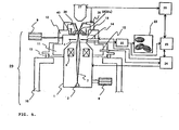
- Fig. 1 is a schematic diagram of a sample inspection apparatus according to the present invention.
- the apparatus consists chiefly of an optical microscope 27, a manipulator 26, and an electron beam apparatus section 29 located under a sample holder 40.
- the electron beam apparatus section 29 includes an electron optical column 1 forming primary beam irradiation means.
- An electron gun 2 forming an electron source is disposed in the electron optical column 1 and emits an accelerated electron beam 7 that is a primary beam.
- the electron beam 7 is one kind of charged particle beam.
- the beam 7 is focused by a condenser lens (objective lens) 3.
- the focused electron beam 7 is directed at a liquid sample 20 via a sample-holding film 32 (described later) formed on the sample holder 40.
- the sample 20 is held on the sample holder 40.
- the liquid sample 20 includes biological cells to be inspected and a culture medium surrounding the cells.
- the front-end side of the electron optical column 1 is connected with a vacuum chamber 11.
- the electron gun 2 is mounted in the base side of the column 1.
- the base side of the column 1 is located under the vacuum chamber 11. Because of this configuration, the electron beam 7 released from the electron gun 2 travels upward through the column 1, passes through the space inside the vacuum chamber 11 and through the sample-holding film 32, and reaches the liquid sample 20.
- the electron beam 7 is deflected by deflection means (not shown).
- the beam 7 scans the liquid sample 20.
- the cells contained in the liquid sample 20 are also scanned with the beam 7.
- the electron optical column 1 forms the primary beam irradiation means in this way.
- the column is of the inverted type.
- a backscattered electron detector 4 is mounted on the front-end side of the column 1 inside the vacuum chamber 11.
- the backscattered electron detector 4 detects backscattered electrons produced when the cells included in the liquid sample 20 are irradiated with the electron beam 7.
- a semiconductor detector using a PN junction or a scintillator detector using a YAG crystal is used as the backscattered electron detector 4.
- these detectors amplify even light signals and so if the illuminating light emitted from the optical microscope 27 and impinging on the liquid sample 20 hits the backscattered electron detector 4, a background against the backscattered electron signal is created. Consequently, it is necessary to take care to prevent the illuminating light from hitting the backscattered electron detector 4. Accordingly, in the present invention, light blocking capabilities are imparted to the sample protective film 32.
- the output signal from the backscattered electron detector 4 is sent to an image formation device 22 disposed outside the vacuum chamber 11.
- the image formation device 22 creates image data based on the detector output signal.
- the image data becomes image data corresponding to the SEM image.
- the image data is fed to a display device 23, which in turn displays an image based on the incoming image data.
- the displayed image becomes an SEM image.
- the image data formed by the image formation device 22 is sent to a computer 25.
- the computer 25 image-processes the image data and makes decisions based on the result of the image processing.
- the inside of the electron optical column 1 is pumped down to a desired pressure by vacuum pumping means 8.
- the inside of the vacuum chamber 11 is evacuated to a desired pressure by vacuum pumping means 9.
- the vacuum chamber 11 is placed over a pedestal 10 via a vibration-proofing device 13.
- a sample holder placement portion 12 is formed on top of the vacuum chamber 11 and provided with a hole to permit the electron beam 7 to be directed at the sample-holding film 32.
- the sample holder 40 is placed on the placement portion 12 via an O-ring (not shown). Consequently, the sample holder 40 is withdrawably supported in the vacuum chamber 11.
- a vacuum gauge 15 for detecting the pressure inside the vacuum chamber 11 is installed in the vacuum chamber 11.
- a shutter 14 that is in an open state in Fig. 1 is installed between the front end of the electron optical column 1 and the sample-holding film 32.
- the shutter 14 is automatically moved and closed as shown in Fig. 2 .
- the shutter 14 is moved as shown in Fig. 2 .
- the liquid sample 20 that has flowed into the vacuum chamber 11 can be blocked by the shutter 14. Hence, contamination of the electron microscope column 1 and backscattered electron detector 4 is prevented.
- the shutter 14 is fitted with a catch pan for receiving the liquid sample, it is possible to cope with inflow of a large amount of liquid sample.
- the shutter 14 partitions the vacuum chamber 11 into two vertically separated spaces not completely but partially. Therefore, the shutter 14 is simple in structure and can operate at high speed.
- the shutter can be activated (i.e., a transition from the state of Fig. 1 to the state of Fig. 2 can be made) in 0.1 second after the vacuum gauge 15 detects a pressure rise.
- the shutter can be made thin. Consequently, the distance between the front end of the electron microscope column 1 and the sample-holding film 32 (i.e., the working distance of the SEM) can be reduced. Thus, high resolution can be accomplished.
- the electron beam apparatus section 29 equipped with the electron optical column 1, vacuum chamber 11, shutter 14, and vacuum gauge 15 is controlled by an electron beam controller 24.
- the manipulator 26 for giving a stimulus (such as a voltage, chemical substance, or medicine) to the cells and for moving them if necessary and an optical microscope 27 are placed on the sample holder placement portion 12.
- the microscope 27 permits one to observe the cells and to check the position of the manipulator 26.
- the optical axis of the optical microscope 27 is coincident with the optical axis of the electron beam 7.
- the center of field of view of the optical microscope 27 is coincident with the center of field of view of the SEM image.
- a region observed by the optical microscope can be made substantially coincident with the SEM image.
- the field of view of the SEM image and the field of view of the optical microscope 27 can be adjusted by manipulating the manipulator 26 or moving the sample holder placement portion 12 on which the sample holder 40 is placed by means of a moving mechanism (not shown).
- the sample inspection apparatus has the electron beam apparatus section 29, manipulator 26, optical microscope 27, electron beam controller 24, overall controller 28, image formation device 22, and display device 23. These portions are connected with the computer 25. Information can be exchanged between these portions.
- the sample holder 40 is constructed as shown in Fig. 3 .
- the sample holder 40 is composed of a dish-like body portion 37 made of plastic or glass and a film holder (frame-like member) 18 on which the sample-holding film 32 is formed.
- the film 32 transmits the electron beam 7.
- the body portion 37 has light-blocking capabilities to prevent the illuminating light from the optical microscope 7 from hitting the backscattered electron detector 4.
- a recessed portion is formed inside the body portion 37. The bottom surface of the recessed portion forms a sample-holding surface 37a that is open.
- the sample-holding surface 37a of the body portion 37 is (centrally in the example of Fig. 3 ) provided with a through-hole 37b.
- a step portion 37c is formed around the hole 37b on the side of the sample-holding surface 37a.
- the film holder 18 is disposed on the step portion 37c and has the sample-holding film 32.
- the sample-holding film 32 has a first surface 32a that forms the sample-holding surface 37a.
- the sample-holding surface 37a is substantially flush with the sample-holding surface 37a of the body portion 37. Consequently, at least a part of the sample-holding surface 37a of the sample holder 40 is formed by the sample-holding film 32.
- Tapering portions 37d are formed on the side of the hole 37b on the opposite side of the sample-holding surface 37a.
- the tapering portions 37d are spread apart toward the surface on the opposite side of the sample-holding surface 37a.
- the spread angle is set to 90° to 120°.
- a region of the lower surface of the sample holder 40 might be exposed to a vacuum ambient and become irradiated with the electron beam 7.
- a conductive film 301 is formed on this region to prevent charging of the sample holder 40 when it is irradiated with the beam 7.
- the conductive film 301 is in contact with the film holder 18. Electric charge accumulated by being irradiated with the electron beam 7 can be dissipated away to the liquid sample 20 via the filmholder 18 made of silicon.
- the presence of the conductive film 301 reduces the charging of the lower surface of the sample holder 40 and can prevent displacement of the orbit of the beam 7 (that would normally be produced when the liquid sample 20 is irradiated with the beam 7) and distortion and illumination spots in the SEM image that would be normally produced by displacement of the orbit of backscattered electrons.
- the conductive film 301 can be formed, for example, by vapor-depositing aluminum or gold or applying silver paste.
- the conductive film 301 acts also to prevent the illuminating light of the optical microscope from hitting the backscattered electron detector.
- the structure of the film holder 18 is shown in Fig. 4 .
- the sample-holding film 32 is formed on a silicon substrate 34.
- a first surface 32a of the sample-holding film 32 (lower surface as viewed in Fig. 4 ; upper surface as viewed in Fig. 3 ) is exposed.
- the liquid sample 20 containing a liquid such as a culture medium and a specimen to be inspected such as cells is placed on the first surface (sample-holding surface) 32a of the sample-holding film 32. Since the first surface 32a is under atmospheric pressure, evaporation of moisture from the liquid sample 20 can be suppressed to a minimum.
- the silicon substrate 34 is centrally provided with an opening 34a (upper surface in Fig. 4 ; lower surface in Figs. 1 and 3 ) covered with the sample-holding film 32.
- a central portion of the second surface 32b of the sample-holding film 32 is exposed to the inside ambient of the vacuum chamber 11 through the opening 34a.
- the first surface 32a of the sample-holding film 32 is exposed to the atmospheric-pressure ambient, while the second surface 32b is exposed to the vacuum ambient.
- the film 32 is supported and reinforced with a lattice 35.
- a method of creating the film holder 18 is next described by referring to Fig. 5 .
- a film of Al 509 is formed on a silicon substrate 501 using sputtering or vacuum vapor deposition.
- silicon nitride films 502 and 503 are formed using CVD (chemical vapor deposition).
- a typical thickness of the Al film 509 is 30 nm.
- a typical thickness of the silicon nitride film 502 is 30 nm.
- Layers of resist 504 and 505 are applied on the silicon nitride films 502 and 503, respectively ( Fig. 5(b) ).
- the layer of resist 505 is patterned photolithographically to leave behind resist layer portions 505a ( Fig. 5(c) ).
- the silicon nitride film 503 is processed by dry etching, and silicon nitride film portions 503a are left behind ( Fig. 5(d) ).
- the silicon substrate 501 is wet-etched with KOH to form an opening 510 ( Fig. 5(e) ).
- the resist layer portions 504 and 505a are removed by ashing ( Fig. 5(f) ).
- Resist 506 is applied on the layer of silicon nitride film 502 ( Fig. 5(g) ).
- a layer of metal 507 of Al or Ni is formed to a thickness of 1 ⁇ m on the opposite side of the silicon nitride film 502 ( Fig. 5(h) ).
- Resist 508 is applied on the metal layer 507, and a pattern is photolithographically formed using a mask ( Fig. 5(i) ).
- the resist layer 508 is etched ( Fig. 5(j) ).
- the resist layer 508 is removed by ashing or organic cleaning (Fig. 5(k)). As a result, the opening 34a and lattice 35 are formed.
- the film holder 18 fabricated in this way is inverted up and down from the state of Fig. 4 .
- the first surface 32a (silicon nitride film 502) of the sample-holding film 32 composed of the Al film 509 and silicon nitride film 502 is taken as an upper surface.
- the second surface 32b (Al film 509) can also be taken as an upper surface.
- the film in contact with the cells is a metal
- metal ions may adversely affect the cells.
- the sample-holding film 32 contains the metallic film of Al, light can be blocked. Consequently, the illuminating light used in the optical microscope does not hit the backscattered electron detector 4. As a result, the backscattered electron image of the sample containing cells is free from a background signal due to the illuminating light.
- the film holder 18 is firmly attached to the step portion 37c over the hole 37b formed in the body portion 37 forming the sample holder 40.
- the sample holder 40 is fabricated ( Fig. 3 ).
- bonding using an epoxy-based or silicone-based adhesive or fusion making use of heat, ultrasonic waves, or a laser beam can be used. Consequently, the film holder 18 is firmly held in a position corresponding to the hole 37b in the sample-holding surface 37a of the body portion 37.
- the body portion 37 and film holder 18 are combined to fabricate the sample holder 40.
- the sample-holding film 32 may be directly firmly bonded to the body portion 37.
- the body portion 37 and the sample-holding film 32 maybe fabricated integrally.
- cell adhesion molecules acting as molecules for bonding the sample may be applied to the sample-holding surface 37a including the first surface 32a of the sample-holding film 32.
- the total thickness of the silicon nitride film 502 and Al film 509 is set within a range of from 20 to 1, 000 nm.
- the thickness of the Al film 509 is set to 10 to 100 nm to block light.
- the sample-holding film 32 of the film holder 18 is made of silicon nitride.
- the film 32 may be made of silicon oxide, boron nitride, polymer, polyethylene, polyimide, polypropylene, or carbon. Even where films of these materials are used, their film thicknesses are set within a range of from 10 to 1,000 nm.
- the film 509 may be made of Be or Mg instead of Al. In order to prevent scattering of the electron beam, it is desired that the material have a low atomic number.
- the sample-holding film 32 made of the aforementioned material transmits the electron beam 7 but does not transmit gas or liquid. Moreover, it is highly desirable that the film be capable of withstanding a pressure difference of at least 1 atmosphere across the opposite surfaces. As the thickness of the sample-holding film 32 is reduced, scattering of the electron beam 7 is reduced and, therefore, the resolution is improved but the film is more easily damaged. As the thickness is increased, scattering of the electron beam 7 increases, resulting in decreased resolution. However, the film is less likely to be damaged.
- the preferable thickness of the film is 20 to 200 nm.
- FIG. 3 An inspection method according to one embodiment of the present invention is next described.
- cells 38 to be inspected are cultured within a culture medium 39 using the sample holder 40.
- the culture medium is Product No. D5796 of Sigma-Aldrich Co., for example.
- the culture medium is discarded from the laboratory dish where the cells have been previously cultured.
- a mixture liquid of trypsin and EDTA (ethylenediaminetetraacetic acid) is put into the dish to peel off the cells adsorbed to the dish.
- the peeled cells are then recovered into a centrifuge tube, and a culture medium is added.
- the trypsin is inactivated and then the cells are spun down.
- the supernatant fluid is discarded from the centrifuge tube and the remaining liquid is stirred in the culture medium.
- a part (e.g. , 1/10) of the stirred liquid including the cells 38 is entered into the sample holder 40.
- More culture medium 39 (reagent solution) is added.
- the holder is allowed to stand still in a cell culture chamber. After a lapse of several hours, the cells 38 begin to be adsorbed onto the sample-holding surface 37a of the sample holder 40 including the first surface 32a of the sample-holding film 32 and proliferate.
- the aforementioned method maybe modified according to cells and is merely shown as one example. Consequently, the cells 38 to be observed or inspected are cultured within the sample holder 40. It follows that the liquid sample 20 containing the cultured cells 38 and culture medium 39 is constituted.
- cell adhesion molecules are applied to the sample-holding surface 37a of the sample holder 40 (especially, the first surface 32a (sample-holding surface) of the sample-holding film 32 observed with an electron beam), cultivation is facilitated.
- the cell adhesion molecules cause cells arranged for cultivation and cells proliferated by cultivation to be adsorbed onto the sample-holding surface.
- the cell adhesion molecules include collagen, fibronectin, vitronetin, cadherin, integrin, claudins, desmogleins, neuroligin, neurexin, selectin, laminins, and poly-L-lysine.
- the sample holder 40 is placed on the holder placement portion 12. At this time, the shutter 14 is closed and in the state of Fig. 2 . Then, the insides of the vacuum chamber 11 and electron optical column 1 are pumped down to desired degrees of vacuum using pumping means 8 and 9.
- the pressure inside the vacuum chamber 11 is set to about 1 Pa.
- the pressure inside the electron optical column 1 (especially, around the electron gun 2) is set to about 10 -4 to 10 -5 Pa, for example.
- the positions of the cells 38 and of the manipulator 26 are checked with the optical microscope 27.
- a glass microtube holding microelectrodes therein is installed at the front end of the manipulator.
- a voltage can be applied to the cells through the microelectrodes.
- a liquid can be made to flow in and out through the glass microtube.
- the manipulator 26 is moved while making an observation with the optical microscope 27 to bring the cells 38 close to the glass microtube. Then, a negative pressure is applied to the glass microtube to bring it into intimate contact with the cell membranes. As a result, potential response can be measured.
- the manipulator 26 When the manipulator 26 is moved as described above, if the sample-holding film 32 is erroneously damaged and the liquid sample 20 enters the vacuum chamber 11, the sample 20 can be blocked by the shutter 14 because the shutter 14 is closed. Consequently, the contamination of the electron optical column 1 is prevented. Where the shutter 14 is not present, the liquid sample 20 enters the electron optical column 1. This makes it necessary to clean the apparatus. At times, the apparatus is made unusable.
- the electron beam 7 is directed at these portions of the liquid sample 20 including the cells 38 from the electron optical column 1 to perform imaging.
- the beam 7 passes through the sample-holding film 32 of the sample holder 40 and hits the cells 38.
- Backscattered electrons produced from the cells 38 in response to the irradiation are detected by the backscattered electron detector 4.
- the aforementioned tapering portions 37d are formed around the hole 37b of the body portion 37 forming the sample holder 40, collision of the backscattered electrons against the inner side surface of the hole 37b can be suppressed to a minimum. That is, the backscattered electrons can be suppressed from being blocked. The backscattered electrons can be detected efficiently by the backscattered electron detector 4.
- a detection signal produced from the backscattered electron detector 4 is fed to the image formation device 22, which in turn forms image data based on the detection signal. Based on the image data, an image (SEM image) is displayed on the display device 23. A high-resolution image that cannot be obtained with the optical microscope 27 can be derived.
- the sample-holding film 32 contains the Al film 509, the light illuminating the sample from the optical microscope does not reach the backscattered electron detector present inside the vacuum chamber. Therefore, the sample can be imaged with the optical microscope and SEM simultaneously. In consequence, the behavior occurring immediately after a stimulus is given to the cells is observed with the optical microscope. Where a high-resolution image is required, SEM imaging can be done instantly. For this reason, it is possible to cope with a case where the reaction speed of the cells to the stimulus is high.
- the shutter 14 is closed to prevent contamination of the electron optical column 1 if the sample-holding film 32 should be destroyed.
- an observation may be made with the optical microscope 27.
- risk of contamination occurring when the sample-holding film 32 is broken can be reduced.
- the probability of contamination of the inside of the apparatus can be reduced by shortening the interval for which the shutter 14 is opened during inspection.
- the shutter 14 may be once closed.
- the shutter 14 may be again opened at a time when a reaction is deemed to have taken place. Then, imaging may be performed using the electron beam 7.
- the reaction can be checked with the optical microscope 27.
- the shutter 14 and backscattered electron detector 4 are designed separately.
- the backscattered electron detector 4 is mounted at the front end of the shutter 14. When the shutter 14 is open, the backscattered electron detector 4 is located immediately above the electron optical column 1. The efficiency at which backscattered electrons are detected is maximized.
- the manipulator 26 can have a mechanism capable of spraying a chemical substance or medicine into the liquid sample 20. Behavior of the cells 38 in response to the chemical substance or medicine can be observed or inspected while observing the cells by SEM. Furthermore, a function of permitting a liquid to flow out can be imparted to the manipulator 26. This permits the sprayed substance to be recovered. Also, the pH of the culture medium and the osmotic pressure can be maintained constant.
- backscattered electrons are used to form an image.
- Backscattered electrons produce a signal intensity proportional to the atomic number. Therefore, where the specimen is almost totally made of substances of low atomic numbers such as a biological specimen, the image contrast is very low, and it is difficult to improve the resolution.
- a heavy metal such as gold may be adsorbed onto portions of the cells 38 to be noticed in their behavior.
- gold is adsorbed onto the portions (antigen) via an antibody by causing the antigen tagged with gold particles having the nature of being adsorbed on the portions (antigen) to be sprayed against the cells by making use of an antigen-antibody reaction.
- a fluorescent dye or quantum dots e. g. , nanoparticles of Si or particles of CdSe coated with ZnS and having sizes of 10 to 20 nm
- a fluorescent dye or quantum dots that emit light when irradiated with an electron beam may be previously adsorbed onto certain portions of the cells 38, and the emitted light may be observed with an optical microscope.
- normally used gold particles have particle diameters of 10 to 30 nm.
- the adsorptive force between the antibody and gold particles is weak, and gold particles of 10 to 30 nm may not be attached.
- very small gold particles nanogold particles having particle diameters of the order of nanometers are first attached to the antibody. Under this condition, the gold particles are too small and it is difficult to observe them by SEM.
- Silver is adsorbed around the gold particles by making use of a silver sensitizer. This makes it easier to detect them by SEM.
- cells previously cultured in a laboratory dish are taken out and grafted onto the sample holder 40. Then, the cells are cultured.
- cells may be taken from a living organism and directly placed on the sample-holding surface 37a of the sample holder 40. The cells may be cultured in the sample holder 40.
- the use of embodiments of the present invention makes it possible to observe or inspect a specimen via the sample-holding film 32, the specimen being contained in a liquid.
- the use of an open sample chamber facilitates giving a stimulus to cells because access to the sample including a specimen to be inspected can be made from the outside.
- the Al film 509 is formed on a part of the sample-holding film 32 to provide light-blocking capabilities. Illuminating light from the optical microscope 7 canbe prevented from reaching the backscattered electron detector 4. Consequently, the liquid sample 20 can be imaged simultaneously by the optical microscope 7 and electron beam apparatus section (SEM) 29. Even where the response speed of the cells to a stimulus is high, variations in the cells can be observed with the optical microscope. Where a high-resolution image is required, SEM imaging can be done instantly.
- the liquid sample 20 flows into the vacuum chamber 11, increasing the pressure.
- the pressure rise is detected by the vacuum gauge 15. If a pressure higher than 100 Pa, for example, is detected, the information is sent to the electron beam controller 24.
- An instruction for closing the shutter 14 is sent to the shutter 14. As a result, the shutter 14 is closed as shown in Fig. 2 .
- the liquid sample 20 is blocked by the shutter 14. Where the amount of the sample 20 is large, it is possible to prepare a catch pan on the shutter 14. It takes only a short time of 0.1 second until the shutter 14 is closed after the pressure rise is detected.
- the contamination of the electron optical column 1 can be reduced to a level at which the column does not need to be cleaned.
- an electron beam is used as the primary beam. If the sample-holding film 32 shows sufficient shock resistance and strength against impingement of other charged particle beam such as a helium ion beam, the invention can also be applied in a case where the other charged particle beam is used.
- backscattered electrons are used as a secondary signal.
- Information regarding the cells 38 to be inspected can also be obtained by detecting other form of information such as secondary electrons, X-rays, cathodoluminescent light, and electric current absorbed into the cells 38. It is convenient to use the manipulator 26 in measuring the absorption current.
- the sample-holding film 32 of the present embodiment withstand a pressure difference of at least 1 atm. and that gas or liquid do not flow in or out.
- the material of the film 32 includes at least one of polymer, polyethylene, polyimide, polypropylene, carbon, silicon oxide, silicon nitride, and boron nitride together with the metal layer.
- the total film thickness is in a range of from 20 to 1,000 nm.
- the first surface 32a of the film 32 on which the specimen 38 is held is made open to permit access to the specimen 38 from the outside using a manipulator or the like.
- the first surface 32a of the film 32 is the upper surface of the film 32
- the second surface 32b of the film 32 is the lower surface of the film 32.
- the film 32 contains a metal layer and a layer made of at least one of polymer, polyethylene, polyimide, polypropylene, carbon, silicon oxide, silicon nitride, and boron nitride.
- the total thickness of these layers can be set within a range of from 20 to 1,000 nm.
- the thickness of the metal layer can be set within a range of from 10 to 100 nm.
- the metal layer can be made of Be, Mg, or Al.
- the metal layer can be located not on a side of the first surface 32a of the film 32.
- the primary charged particle beam can be an electron beam.
- the secondary signal can be at least any one type of backscattered electrons, secondary electrons, absorption current, cathodoluminescent light, and X-rays.
Landscapes
- Chemical & Material Sciences (AREA)
- Analytical Chemistry (AREA)
- Physics & Mathematics (AREA)
- Health & Medical Sciences (AREA)
- Life Sciences & Earth Sciences (AREA)
- Biochemistry (AREA)
- General Health & Medical Sciences (AREA)
- General Physics & Mathematics (AREA)
- Immunology (AREA)
- Pathology (AREA)
- Analysing Materials By The Use Of Radiation (AREA)
- Investigating, Analyzing Materials By Fluorescence Or Luminescence (AREA)
Claims (18)
- Untersuchungsvorrichtung, umfassend:einen Probenhalter (40), umfassend einen schalenartigen Körperabschnitt (37) und ein rahmenartiges Element (18), wobei der schalenartige Körperabschnitt (37) im Inneren einen Aussparungsabschnitt aufweist, und wobei der Probenhalter ferner einen leitfähigen Film (301) aufweist, welcher mit dem rahmenartigen Element in Kontakt steht, wobei das rahmenartige Element (18) eine mit einem Film (32) bedeckte Öffnung (34a) aufweist, welche eine erste Fläche aufweist, die eine Probenhaltefläche bildet, und an dem Aussparungsabschnitt des Körperabschnitts (37) angeordnet ist;Primärstrahl-Bestrahlungsmittel (2) zum Bestrahlen der zu untersuchenden Probe mit einem Primärstrahl (7) geladener Teilchen durch den Film (32) hindurch;Signal-Detektierungsmittel (4) zum Detektieren eines von der Probe als Reaktion auf die Primärstrahl-Bestrahlung erzeugten Sekundärsignals;wobei der leitfähige Film (301) auf einer Fläche des Probenhalters gebildet ist, welche mit dem Primärstrahl bestrahlt wird;Optisches-Bild-Erfassungsmittel (27) zum Erhalten eines optischen Bildes der Probe durch Beleuchten der Probe mit Licht;wobei die Primärstrahl-Bestrahlungsmittel (2) und die Optisches-Bild-Erfassungsmittel (27) an sich gegenüberliegenden Seiten des Films (32) angeordnet sind; undwobei die Vorrichtung derart eingerichtet ist, dass während einer Untersuchung die erste Fläche des Films (32), welche die Probe hält, einer Atmosphärendruck-Umgebung ausgesetzt ist, und der Film (32) und der leitfähige Film (301) zum Blockieren des Lichts dienen.
- Untersuchungvorrichtung nach Anspruch 1, ferner umfassend eine Vakuumkammer (11) zum Vermindern des Drucks einer Umgebung, welche mit einer zweiten Fläche (32b) des Films (32) in Kontakt steht.
- Untersuchungsvorrichtung nach einem der Ansprüche 1 und 2, wobei die erste Fläche (32a) des Films (32), auf welcher die Probe gehalten ist, offen ausgestaltet ist, um einen Zugang zu der Probe von außen zu erlauben.
- Untersuchungsvorrichtung nach einem der Ansprüche 1 bis 3, wobei die erste Fläche (32a) des Films (32) eine obere Fläche des Films ist, während eine zweite Fläche (32b) des Films eine untere Fläche des Films ist.
- Untersuchungsvorrichtung nach einem der Ansprüche 1 bis 4, wobei der Film (32) eine wenigstens aus einem von Polymer, Polyethylen, Polyimid, Polypropylen, Kohlenstoff, Siliciumoxid, Siliciumnitrid und Bornitrid hergestellte Schicht und eine Metallschicht umfasst, und wobei eine Gesamtdicke dieser Schichten in einem Bereich von 20 bis 1000 nm liegt.
- Untersuchungvorrichtung nach Anspruch 5, wobei die Metallschicht eine Dicke von 10 bis 100 nm aufweist.
- Untersuchungvorrichtung nach einem der Ansprüche 5 und 6, wobei die Metallschicht aus Be, Mg oder Al hergestellt ist.
- Untersuchungvorrichtung nach einem der Ansprüche 5 bis 7, wobei die Metallschicht nicht auf einer Seite der ersten Fläche (32a) des Films (32) angeordnet ist.
- Untersuchungsvorrichtung nach einem der Ansprüche 1 bis 8, wobei der Primärstrahl ein Elektronenstrahl ist, und wobei das Sekundärsignal wenigstens eine Art von rückgestreuten Elektronen, Sekundärelektronen, Absorptionsstrom, Kathoden-Lumineszenz-Licht und Röntgenstrahlen ist.
- Untersuchungsverfahren, umfassend die Schritte:Vorbereiten eines Probenhalters (40), umfassend einen schalenartigen Körperabschnitt (37) und ein rahmenartiges Element (18), wobei der schalenartige Körperabschnitt (37) im Inneren einen Aussparungsabschnitt aufweist, sowie einen leitfähigen Film (301), welcher mit dem rahmenartigen Element in Kontakt steht, wobei das rahmenartige Element (18) eine mit einem Film (32) bedeckte Öffnung (34a) aufweist und an dem Aussparungsabschnitt des Körperabschnitts (37) angeordnet ist, wobei der Film (32) eine erste Fläche (32a) und eine zweite Fläche (32b) aufweist;Halten einer zu untersuchenden Probe auf der ersten Fläche (32a) des Films (32);Bestrahlen der Probe mit einem Primärstrahl (7) geladener Teilchen durch den Film (32) hindurch von einer Seite der zweiten Fläche des Films her; wobei der leitfähige Film an einer Fläche des Probenhalters gebildet ist, welche mit dem Primärstrahl bestrahlt wird;Detektieren eines Sekundärsignals, welches von der Probe in Reaktion auf die Primärstrahl-Bestrahlung erzeugt wird; undBeleuchten der Probe mit Licht von einer Seite der ersten Fläche des Films (32) her und Erhalten eines optischen Bildes der Probe;wobei während einer Untersuchung die Probe auf der ersten Fläche (32a) des Films (32) einer Atmosphärendruck-Umgebung ausgesetzt wird, und der Film (32) und der leitfähige Film (301) zum Blockieren des Lichts dienen.
- Untersuchungsverfahren nach Anspruch 10, ferner umfassend den Schritt:Vermindern des Drucks einer Umgebung, welche mit der zweiten Fläche (32b) des Films (32) in Kontakt steht.
- Untersuchungsverfahren nach einem der Ansprüche 10 und 11, wobei die erste Fläche (32a) des Films (32), auf welcher die Probe gehalten wird, offen ausgestaltet ist, um einen Zugang zu der Probe von außen zu erlauben.
- Untersuchungsverfahren nach einem der Ansprüche 10 bis 12, wobei die erste Fläche (32a) des Films (32) eine obere Fläche des Films ist, während die zweite Fläche (32b) des Films eine untere Fläche des Films ist.
- Untersuchungsverfahren nach einem der Ansprüche 10 bis 13, wobei der Film (32) eine wenigstens aus einem von Polymer, Polyethylen, Polyimid, Polypropylen, Kohlenstoff, Siliciumoxid, Siliciumnitrid und Bornitrid hergestellte Schicht und eine Metallschicht umfasst, und wobei eine Gesamtdicke dieser Schichten in einem Bereich von 20 bis 1000 nm liegt.
- Untersuchungverfahren nach Anspruch 14, wobei die Metallschicht eine Dicke von 10 bis 100 nm aufweist.
- Untersuchungverfahren nach einem der Ansprüche 14 und 15, wobei die Metallschicht aus Be, Mg oder Al hergestellt ist.
- Untersuchungverfahren nach einem der Ansprüche 14 bis 16, wobei die Metallschicht nicht auf einer Seite der ersten Fläche (32a) des Films (32) angeordnet ist.
- Untersuchungsverfahren nach einem der Ansprüche 10 bis 17, wobei der Primärstrahl (7) ein Elektronenstrahl ist, und wobei das Sekundärsignal wenigstens eine Art von rückgestreuten Elektronen, Sekundärelektronen, Absorptionsstrom, Kathoden-Lumineszenz-Licht und Röntgenstrahlen ist.
Applications Claiming Priority (1)
| Application Number | Priority Date | Filing Date | Title |
|---|---|---|---|
| JP2008101990A JP2009250904A (ja) | 2008-04-10 | 2008-04-10 | 検査装置及び検査方法 |
Publications (3)
| Publication Number | Publication Date |
|---|---|
| EP2108947A2 EP2108947A2 (de) | 2009-10-14 |
| EP2108947A3 EP2108947A3 (de) | 2010-08-25 |
| EP2108947B1 true EP2108947B1 (de) | 2013-10-30 |
Family
ID=40934937
Family Applications (1)
| Application Number | Title | Priority Date | Filing Date |
|---|---|---|---|
| EP08254165.7A Not-in-force EP2108947B1 (de) | 2008-04-10 | 2008-12-24 | Vorrichtung und Verfahren zur Inspektion |
Country Status (3)
| Country | Link |
|---|---|
| US (1) | US7968843B2 (de) |
| EP (1) | EP2108947B1 (de) |
| JP (1) | JP2009250904A (de) |
Families Citing this family (9)
| Publication number | Priority date | Publication date | Assignee | Title |
|---|---|---|---|---|
| JP5215701B2 (ja) * | 2008-03-26 | 2013-06-19 | 日本電子株式会社 | 試料検査装置及び試料検査方法 |
| JP2010230417A (ja) * | 2009-03-26 | 2010-10-14 | Jeol Ltd | 試料の検査装置及び検査方法 |
| JP5115997B1 (ja) * | 2011-12-27 | 2013-01-09 | 独立行政法人産業技術総合研究所 | 走査型電子顕微鏡像観察用の試料支持部材及び走査型電子顕微鏡像の観察方法 |
| US8791438B2 (en) * | 2012-07-27 | 2014-07-29 | Gatan Inc. | Ion beam sample preparation apparatus and methods |
| NL2013262B1 (en) | 2014-07-25 | 2016-09-09 | Delmic B V | Method for inspecting a sample using an assembly comprising a scanning electron microscope and a light microscope. |
| CN106770405A (zh) * | 2016-12-09 | 2017-05-31 | 清华大学 | 一种完全大气压下超光学衍射成像装置 |
| CN107917924B (zh) * | 2017-10-10 | 2020-01-10 | 中国科学院自动化研究所 | 低能量背散射电子探测器 |
| CN107976458A (zh) * | 2017-10-10 | 2018-05-01 | 中国科学院自动化研究所 | 低能量背散射电子探测器 |
| CN121013972A (zh) * | 2023-03-29 | 2025-11-25 | 光原创新科技有限公司 | 用于承载生物样品以供光学显微镜观察的带有fep薄膜的样品容器 |
Citations (6)
| Publication number | Priority date | Publication date | Assignee | Title |
|---|---|---|---|---|
| US4349242A (en) * | 1980-02-15 | 1982-09-14 | Nihon Denshi Kabushiki Kaisha | Specimen observation apparatus including an optical microscope and a scanning electron microscope |
| US6552341B1 (en) * | 1999-04-09 | 2003-04-22 | Centre National D'etudes Spatiales | Installation and method for microscopic observation of a semiconductor electronic circuit |
| WO2003104846A2 (en) * | 2002-06-05 | 2003-12-18 | Quantomix Ltd. | A sample enclosure for a scanning electron microscope and methods of use thereof |
| EP1655597A1 (de) * | 2004-11-09 | 2006-05-10 | FEI Company | Verfahren zur Lokalisierung von Fluoreszenzmarkers |
| US20070145267A1 (en) * | 2005-12-12 | 2007-06-28 | Adler David L | Portable scanning electron microscope |
| JP2007294365A (ja) * | 2006-04-27 | 2007-11-08 | Jeol Ltd | 試料検査方法、試料保持体、及び試料検査装置並びに試料検査システム |
Family Cites Families (12)
| Publication number | Priority date | Publication date | Assignee | Title |
|---|---|---|---|---|
| JPS4847394A (de) * | 1971-10-15 | 1973-07-05 | ||
| JP2781320B2 (ja) | 1993-01-18 | 1998-07-30 | 株式会社蛋白工学研究所 | 電子顕微鏡等の試料ホルダ |
| JPH0798285A (ja) * | 1993-09-29 | 1995-04-11 | Ricoh Co Ltd | X線評価装置 |
| EP1426824A1 (de) * | 2002-12-04 | 2004-06-09 | ASML Netherlands B.V. | Lithographischer Apparat, Verfahren zur Herstellung eines Artikels und damit hergestellter Artikel |
| KR101065074B1 (ko) * | 2004-01-16 | 2011-09-15 | 삼성전자주식회사 | 투과전자현미경 성분 맵핑용 표준시료 및 이를 이용한 투과전자현미경 성분 맵핑방법 |
| JP2007294364A (ja) | 2006-04-27 | 2007-11-08 | U Corporation | スイッチガードの製造方法 |
| JP2007292702A (ja) * | 2006-04-27 | 2007-11-08 | Jeol Ltd | 試料検査装置及び試料検査方法並びに試料検査システム |
| JP2008047411A (ja) * | 2006-08-15 | 2008-02-28 | Jeol Ltd | 試料保持体及び試料検査方法並びに試料検査装置 |
| JP5002273B2 (ja) * | 2007-01-23 | 2012-08-15 | 日本電子株式会社 | 試料検査装置及び試料検査方法 |
| EP1936363A3 (de) * | 2006-12-19 | 2010-12-08 | JEOL Ltd. | Vorrichtung, Verfahren und System zur Probenuntersuchung |
| JP2008153086A (ja) * | 2006-12-19 | 2008-07-03 | Jeol Ltd | 試料検査装置及び試料検査方法並びに試料検査システム |
| JP5318364B2 (ja) * | 2007-01-31 | 2013-10-16 | 日本電子株式会社 | 試料保持体、試料検査装置及び試料検査方法、並びに試料保持体の製造方法 |
-
2008
- 2008-04-10 JP JP2008101990A patent/JP2009250904A/ja active Pending
- 2008-12-24 EP EP08254165.7A patent/EP2108947B1/de not_active Not-in-force
-
2009
- 2009-01-06 US US12/349,195 patent/US7968843B2/en not_active Expired - Fee Related
Patent Citations (6)
| Publication number | Priority date | Publication date | Assignee | Title |
|---|---|---|---|---|
| US4349242A (en) * | 1980-02-15 | 1982-09-14 | Nihon Denshi Kabushiki Kaisha | Specimen observation apparatus including an optical microscope and a scanning electron microscope |
| US6552341B1 (en) * | 1999-04-09 | 2003-04-22 | Centre National D'etudes Spatiales | Installation and method for microscopic observation of a semiconductor electronic circuit |
| WO2003104846A2 (en) * | 2002-06-05 | 2003-12-18 | Quantomix Ltd. | A sample enclosure for a scanning electron microscope and methods of use thereof |
| EP1655597A1 (de) * | 2004-11-09 | 2006-05-10 | FEI Company | Verfahren zur Lokalisierung von Fluoreszenzmarkers |
| US20070145267A1 (en) * | 2005-12-12 | 2007-06-28 | Adler David L | Portable scanning electron microscope |
| JP2007294365A (ja) * | 2006-04-27 | 2007-11-08 | Jeol Ltd | 試料検査方法、試料保持体、及び試料検査装置並びに試料検査システム |
Also Published As
| Publication number | Publication date |
|---|---|
| US7968843B2 (en) | 2011-06-28 |
| EP2108947A2 (de) | 2009-10-14 |
| EP2108947A3 (de) | 2010-08-25 |
| JP2009250904A (ja) | 2009-10-29 |
| US20090256074A1 (en) | 2009-10-15 |
Similar Documents
| Publication | Publication Date | Title |
|---|---|---|
| EP2312302A1 (de) | Vorrichtung und Verfahren zur Untersuchung von Proben | |
| EP2105727B1 (de) | Rasterelektronenmikroskop mit einem Film als Probenhalter und einer Schale zum Auffangen von Probenmaterial eines beschädigten Films | |
| US7745802B2 (en) | Specimen holder, specimen inspection apparatus, specimen inspection method, and method of fabricating specimen holder | |
| EP2108947B1 (de) | Vorrichtung und Verfahren zur Inspektion | |
| EP2388575A1 (de) | Probenhalter, Untersuchungsvorrichtung und Untersuchungsverfahren | |
| US8030622B2 (en) | Specimen holder, specimen inspection apparatus, and specimen inspection method | |
| EP2108946B1 (de) | Prüfverfahren und Reagenzlösung | |
| US8530856B2 (en) | Beam device system comprising a particle beam device and an optical microscope | |
| AU2002221019B2 (en) | Device and method for the examination of samples in a non-vacuum environment using a scanning electron microscope | |
| EP2148359A2 (de) | Probenhalter, Probenprüfvorrichtung und Probenprüfverfahren | |
| KR102207711B1 (ko) | 시료 관찰 장치 및 방법 | |
| EP1953793B1 (de) | Probenhalter, Probenprüfvorrichtung, Probenprüfverfahren und Verfahren zur Herstellung des Probenhalters | |
| CN116997989A (zh) | 试样支架以及电子显微镜 | |
| JP5362423B2 (ja) | 試料検査方法及び試料検査装置 |
Legal Events
| Date | Code | Title | Description |
|---|---|---|---|
| PUAI | Public reference made under article 153(3) epc to a published international application that has entered the european phase |
Free format text: ORIGINAL CODE: 0009012 |
|
| AK | Designated contracting states |
Kind code of ref document: A2 Designated state(s): AT BE BG CH CY CZ DE DK EE ES FI FR GB GR HR HU IE IS IT LI LT LU LV MC MT NL NO PL PT RO SE SI SK TR |
|
| AX | Request for extension of the european patent |
Extension state: AL BA MK RS |
|
| PUAL | Search report despatched |
Free format text: ORIGINAL CODE: 0009013 |
|
| AK | Designated contracting states |
Kind code of ref document: A3 Designated state(s): AT BE BG CH CY CZ DE DK EE ES FI FR GB GR HR HU IE IS IT LI LT LU LV MC MT NL NO PL PT RO SE SI SK TR |
|
| AX | Request for extension of the european patent |
Extension state: AL BA MK RS |
|
| RIC1 | Information provided on ipc code assigned before grant |
Ipc: H01J 37/28 20060101ALI20100719BHEP Ipc: G01N 23/22 20060101AFI20090812BHEP Ipc: H01J 37/20 20060101ALI20100719BHEP |
|
| 17P | Request for examination filed |
Effective date: 20110110 |
|
| AKX | Designation fees paid |
Designated state(s): CH DE FR GB LI |
|
| 17Q | First examination report despatched |
Effective date: 20111208 |
|
| RIC1 | Information provided on ipc code assigned before grant |
Ipc: H01J 37/28 20060101ALI20130321BHEP Ipc: H01J 37/20 20060101ALI20130321BHEP Ipc: H01J 37/22 20060101ALI20130321BHEP Ipc: G01N 23/22 20060101AFI20130321BHEP |
|
| GRAP | Despatch of communication of intention to grant a patent |
Free format text: ORIGINAL CODE: EPIDOSNIGR1 |
|
| INTG | Intention to grant announced |
Effective date: 20130514 |
|
| RIN1 | Information on inventor provided before grant (corrected) |
Inventor name: NISHIYAMA, HIDETOSHI |
|
| GRAS | Grant fee paid |
Free format text: ORIGINAL CODE: EPIDOSNIGR3 |
|
| GRAA | (expected) grant |
Free format text: ORIGINAL CODE: 0009210 |
|
| AK | Designated contracting states |
Kind code of ref document: B1 Designated state(s): CH DE FR GB LI |
|
| REG | Reference to a national code |
Ref country code: GB Ref legal event code: FG4D |
|
| REG | Reference to a national code |
Ref country code: CH Ref legal event code: EP Ref country code: CH Ref legal event code: NV Representative=s name: KIRKER AND CIE S.A., CH |
|
| REG | Reference to a national code |
Ref country code: DE Ref legal event code: R096 Ref document number: 602008028409 Country of ref document: DE Effective date: 20131224 |
|
| REG | Reference to a national code |
Ref country code: DE Ref legal event code: R097 Ref document number: 602008028409 Country of ref document: DE |
|
| PLBE | No opposition filed within time limit |
Free format text: ORIGINAL CODE: 0009261 |
|
| STAA | Information on the status of an ep patent application or granted ep patent |
Free format text: STATUS: NO OPPOSITION FILED WITHIN TIME LIMIT |
|
| 26N | No opposition filed |
Effective date: 20140731 |
|
| REG | Reference to a national code |
Ref country code: DE Ref legal event code: R097 Ref document number: 602008028409 Country of ref document: DE Effective date: 20140731 |
|
| REG | Reference to a national code |
Ref country code: FR Ref legal event code: PLFP Year of fee payment: 8 |
|
| PGFP | Annual fee paid to national office [announced via postgrant information from national office to epo] |
Ref country code: DE Payment date: 20151215 Year of fee payment: 8 Ref country code: CH Payment date: 20151211 Year of fee payment: 8 Ref country code: GB Payment date: 20151223 Year of fee payment: 8 |
|
| PGFP | Annual fee paid to national office [announced via postgrant information from national office to epo] |
Ref country code: FR Payment date: 20151110 Year of fee payment: 8 |
|
| REG | Reference to a national code |
Ref country code: DE Ref legal event code: R119 Ref document number: 602008028409 Country of ref document: DE |
|
| REG | Reference to a national code |
Ref country code: CH Ref legal event code: PL |
|
| GBPC | Gb: european patent ceased through non-payment of renewal fee |
Effective date: 20161224 |
|
| REG | Reference to a national code |
Ref country code: FR Ref legal event code: ST Effective date: 20170831 |
|
| PG25 | Lapsed in a contracting state [announced via postgrant information from national office to epo] |
Ref country code: FR Free format text: LAPSE BECAUSE OF NON-PAYMENT OF DUE FEES Effective date: 20170102 Ref country code: CH Free format text: LAPSE BECAUSE OF NON-PAYMENT OF DUE FEES Effective date: 20161231 Ref country code: LI Free format text: LAPSE BECAUSE OF NON-PAYMENT OF DUE FEES Effective date: 20161231 |
|
| PG25 | Lapsed in a contracting state [announced via postgrant information from national office to epo] |
Ref country code: DE Free format text: LAPSE BECAUSE OF NON-PAYMENT OF DUE FEES Effective date: 20170701 Ref country code: GB Free format text: LAPSE BECAUSE OF NON-PAYMENT OF DUE FEES Effective date: 20161224 |